2A3D8-E04Zikr Ring
Umeox Innovations Co., Ltd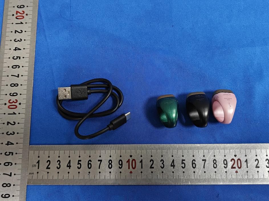
Click to zoom
Application Details
- Equipment Class
- DTS - Digital Transmission System
- Date of Grant
- Jul 24, 2026
- Application Purpose
- Original Equipment
- Equipment Note
- Zikr Ring
- Frequency Range
- 2402.00000000 - 2480.00000000
- Company
- Umeox Innovations Co., Ltd
- Country
- China
Documents & Files
Document Text
Text extracted from the exhibit documents filed with the FCC. Open a document above to read the original.
Attestation Statements
Umeox Innovations Co., Ltd Rev 2026-04-24 Federal Communications Commission Authorization and Evaluation Division 7435 Oakland Mills Road Columbia, MD 21046 USA Date: July 22, 2026 Ref: Attestation Statements Part 2.911(d)(5)(i) and Part 2.911(d)(5)(ii) FCC ID: 2A3D8-E04 Part 2.911(d)(5)(i) [Umeox Innovations Co., Ltd] (“the applicant”) certifies that the equipment for which authorization is sought is not “covered” equipment and does not contain anti-virus software or cybersecurity software prohibited from receiving an equipment authorization pursuant to 47 CFR 2.903, KDB 986446 D01 Covered Equipment Guidance, and FCC Covered List (www.fcc.gov/supplychain/coveredlist). Part 2.911(d)(5)(ii) [Umeox Innovations Co., Ltd] (“the applicant”) certifies that, as of the date of the filing of the application, the applicant is not identified on the Covered List (as a specifically named entity or any of its subsidiaries or affiliates) as an entity producing “covered” equipment. Sincerely, (Applicant signature) (Applicant printed name) Ja son
Attestation Statements
Umeox Innovations Co., Ltd Federal Communications Commission Authorization and Evaluation Division Equipment Authorization Branch 7435 Oakland Mills Road Columbia, MD 21046 [July 23, 2026] U.S. Agent Designation [Umeox Innovations Co., Ltd] acknowledges their consent for the following contact located in the United States to act as their agent for service of process for the equipment for which authorization is sought FCC ID: 2A3D8-E04 Name and company of U.S. agent: [GLOCERTS TECHNOLOGY INC] Physical U.S. address of agent: [19784 SUNKISSED RIDGE DR, RIVERSIDE, CA 92507] FRN of U.S. agent: [0036339737] Email address of U.S. agent: [[email protected]] Telephone of U.S.agent: (626) 588-8039 [GLOCERTS TECHNOLOGY INC] acknowledges their obligation to accept service of process on behalf of [Umeox Innovations Co., Ltd]. [Umeox Innovations Co., Ltd] with the FRN [0031504715] accepts its obligation to maintain an agent for service of process in the United States for no less than 1 year after either the grantee has permanently terminated all marketing and importation of the applicable equipment within the U.S., or the conclusion of any Commission- related administrative or judicial proceeding involving the equipment, whichever is later. By signing this form, we confirm the above and that we are aware of the application requirements listed under § 2.911(d)(7). The information provided in this letter is based on the referenced rule parts of Title 47 of the CFR as well as KDB 986446 D01. Sincerely, Signature Signature [Ja son] [Huiying Fan] [Manager] [Director] [Umeox Innovations Co., Ltd] [GLOCERTS TECHNOLOGY INC]
Cover Letter(s)
Rev 11/20/07 Umeox Innovations Co., Ltd Federal Communications Commission Authorization and Evaluation Division Date: July 22, 2026 Confidentiality Request regarding application for certification of FCC ID: 2A3D8-E04 Pursuant to Sections 0.457 and 0.459 of the Commission’s Rules, we hereby request confidential treatment of information accompanying this application as outlined below: Exhibit Type File Name* Block Diagram BLOCK.pdf Schematics SCH.pdf Operational Description OPC.pdf The above materials contain trade secrets and proprietary information not customarily released to the public. The public disclosure of these materials may be harmful to the applicant and provide unjustified benefits to its competitors. The applicant understands that pursuant to Section 0.457 of the Rules, disclosure of this application and all accompanying documentation will not be made before the date of the Grant for this application. Pursuant to DA04-1705 June 15, 2004 of the Commission’s public notice, we also request temporary confidential treatment of information accompanying this application as outlined below: Exhibit Type File Name* User’s Manual Manual.pdf Internal Photos Internal Photos.pdf ☐ For 45 days, pursuant to Public Notice DA 04-1705. or ☑ For 180 days pursuant to KDB 726920 D01. The applicant understands that pursuant to Section 0.457 of the Rules, disclosure of this application and all accompanying documentation will not be made before the date of the Grant for this application. Sincerely, (signature) (printed name) Ja son
External Photos
Shenzhen CTB Testing Technology Co., Ltd. Report Tel: 4008-707-283 Web: http://www.ctb-lab.net Page 1 of 4 Model: E04 External Photos Shenzhen CTB Testing Technology Co., Ltd. Report Tel: 4008-707-283 Web: http://www.ctb-lab.net Page 2 of 4 Shenzhen CTB Testing Technology Co., Ltd. Report Tel: 4008-707-283 Web: http://www.ctb-lab.net Page 3 of 4 Shenzhen CTB Testing Technology Co., Ltd. Report Tel: 4008-707-283 Web: http://www.ctb-lab.net Page 4 of 4
ID Label/Location Info
FCC ID LABEL: Label Location: FCC ID: 2A3D8-E04
RF Exposure Info
Shenzhen CTB Testing Technology Co., Ltd. FCC ID:2A3D8-E04 Portable device According to §15.247(e)(i) and §1.1307(b)(1), systems operating under the provisions of this section shall be operated in a manner that ensures that the public is not exposed to radio frequency energy level in excess of the Commission’s guidelines. According to KDB447498 D01 General RF Exposure Guidance V06 The 1-g SAR and 10-g SAR test exclusion thresholds for 100 MHz to 6 GHz at test separation distances ≤ 50 mm are determined by: [(max. power of channel, including tune-up tolerance, mW)/(min. test separation distance, mm)]·[√f(GHZ)] ≤ 3.0 for 1-g SAR and ≤ 7.5 for 10-g extremity SAR, where: • f(GHZ) is the RF channel transmit frequency in GHz • Power and distance are rounded to the nearest mW and mm before calculation • The result is rounded to one decimal place for comparison When the minimum test separation distance is < 5 mm, a distance of 5 mm is applied to determine SAR test exclusion. BLE:1M Modulation Channel Freq. (GHz) Conduct ed power (dBm) Conducte d power (mW) Tune-up power (dBm) Max tune-up power (dBm) Max tune-up power (mW) Distance (mm) Result calculatio n SAR Exclusion threshold SAR test exclusion 2.402 2.533 1.79 2±1 3.00 2.00 <5 0.61847 3.00 YES 2.44 2.599 1.82 2±1 3.00 2.00 <5 0.62334 3.00 YES 2.480 2.095 1.62 2±1 3.00 2.00 <5 0.62843 3.00 YES GFSK BLE:2M Modulation Channel Freq. (GHz) Conduct ed power (dBm) Conducte d power (mW) Tune-up power (dBm) Max tune-up power (dBm) Max tune-up power (mW) Distance (mm) Result calculatio n SAR Exclusion threshold SAR test exclusion 2.402 2.656 1.84 2±1 3.00 2.00 <5 0.61847 3.00 YES 2.44 2.745 1.88 2±1 3.00 2.00 <5 0.62334 3.00 YES 2.480 2.256 1.68 2±1 3.00 2.00 <5 0.62843 3.00 YES GFSK Conclusion: For the max result : 0.62843≤ FCC Limit 3.0 for 1g SAR.
Test Report
承 認 書 SPECIFICATION FOR APPROVAL 客戶名稱 CUSTOMER : 客戶料號 CUSTOMER’S P/N : 料號 PART NUMBER : WAN2012F245C04 規格 DESCRIPTION : Chip Antenna 2012 L Ant 2.45G Type 04 版本 VERSION : V1.6 日期 ISSUE DATE : 2021/05/20 客 戶 承 認 CUSTOMER APPROVED 工 程 部 R&D CENTER 承 認 APPROVAL 確 認 CHECKED 製 作 DRAWN Ray Tennyson Snow 萬誠科技股份有限公司 OneWave Electronic Co., Ltd. 112台北市北投區立功街151號1樓 1F, No. 151, Li Gong Street, Beitou District, Taipei City 112, Taiwan 電話: (02) 2898-2220 TEL: +886 2 2898-2220 傳真: (02) 2898-5055 FAX: +886 2 2898-5055 2/11 ONEWAVE TECHNOLOGY CO., LTD. 2012 Chip antenna For Bluetooth / WLAN Applications Dimension (mm) L 2.05 ± 0.20 W 1.23 ± 0.20 T 0.45 ± 0.20 P/N: WAN2012F245C04 3/11 ONEWAVE TECHNOLOGY CO., LTD. Part Number Information WAN 2012 F 245 C 04 A B C D E F A Product Series Antenna B Dimension L x W 2.05X1.23mm ( ± 0.2mm) C Material High K material D Working Frequency 2.4 ~ 2.5GHz E Feeding mode PIFA & Single Feeding F Antenna type Type = 04 1. Electrical Specification Remark : Bandwidth & Peak Gain was measured under evaluation board of next page Specification Part Number WAN2012F245C04 Central Frequency 2450 MHz Bandwidth 85 (Min.) MHz Return Loss -6.5 (Max) dB Peak Gain 1.72 dBi Impedance 50 Ohm Operating Temperature -40~+110 °C Maximum Power 4 W Resistance to Soldering Heats 10 ( @ 260°C) sec. Polarization Linear Azimuth Beamwidth Omni-directional Termination Ni / Au (Leadless) 4/11 ONEWAVE TECHNOLOGY CO., LTD. 2. Recommended PCB Pattern Evaluation Board Dimension (board size 80x40mm) 2 nd Evaluation Board Dimension Evaluation Board Dimension (board size 80x40mm) Suggested Matching Circuit 重要資訊 : 匹配元件建議使用精準度高的電感±0.1~0.3nH、電容±0.1pF 1.0pF 5/11 ONEWAVE TECHNOLOGY CO., LTD. Layout Dimensions in Clearance area( Size=3.0*5.0mm) FootPrint (Unit : mm) ◆ 2 nd Layout Dimensions in Clearance area( Size=8.0*2.5mm) Matching circuit Tuning Component Matching circuit Tuning Compon ent 6/11 ONEWAVE TECHNOLOGY CO., LTD. 3. Measurement Results Return Loss 7/11 ONEWAVE TECHNOLOGY CO., LTD. Radiation Pattern Efficiency Peak Gain Directivity 2400MHz 63.12 % 1.62 dBi 3.61 dBi 2450MHz 70.56 % 1.72 dBi 3.23 dBi 2500MHz 65.48 % 1.64 dBi 3.47 dBi Chamber Coordinate System Z Y X 8/11 ONEWAVE TECHNOLOGY CO., LTD. 4.Reliability and Test Condictions ITEM REQUIREMENTS TEST CONDITION Solderability 1. Wetting shall exceed 90% coverage 2. No visible mechanical damage Pre-heating temperature:150°C/60sec. Solder temperature:230±5°C Duration:4±1sec. Solder:Sn-Ag3.0-Cu0.5 Flux for lead free: rosin Solder heat Resistance 1. No visible mechanical damage 2. Central Freq. change :within ± 6% 10 ± 0.5 sec. 60 sec . . T E M P ( °C ) 150 °C 2 6 0 °C Pre-heating temperature:150°C/60sec. Solder temperature:260±5°C Duration:10±0.5sec. Solder:Sn-Ag3.0-Cu0.5 Flux for lead free: rosin Component Adhesion (Push test) 1. No visible mechanical damage The device should be reflow soldered(230±5°C for 10sec.) to a tinned copper substrate A dynometer force gauge should be applied the side of the component. The device must with-ST-F 0.5 Kg without failure of the termination attached to component. Component Adhesion (Pull test) 1. No visible mechanical damage Insert 10cm wire into the remaining open eye bend ,the ends of even wire lengths upward and wind together. Terminal shall not be remarkably damaged. Thermal shock 1. No visible mechanical damage 2. Central Freq. change :within ±6% Phase Temperature(°C) Time(min) 1 +110±5°C 30±3 2 Room Temperature Within 3sec 3 -40±2°C 30±3 4 Room Temperature Within 3sec +110°C=>30±3min -40°C=>30±3min Test cycle:10 cycles The chip shall be stabilized at normal condition for 2~3 hours before measuring. Resistance to High Temperature 1. No visible mechanical damage 2. Central Freq. change :within ±6% 3. No disconnection or short circuit. Temperature: +110±5°C Duration: 1000±12hrs The chip shall be stabilized at normal condition for 2~3 hours before measuring. Resistance to Low Temperature 1. No visible mechanical damage 2. Central Freq. change :within ±6% 3. No disconnection or short circuit. Temperature:-40±5°C Duration: 1000±12hrs The chip shall be stabilized at normal condition for 2~3 hours before measuring. Humidity 1. No visible mechanical damage 2. Central Freq. change :within ±6% 3. No disconnection or short circuit. Temperature: 40±2°C Humidity: 90% to 95% RH Duration: 1000±12hrs The chip shall be stabilized at normal condition for 2~3 hours before measuring. 4±1 sec. 60sec TEMP (°C) 150°C 230°C 9/11 ONEWAVE TECHNOLOGY CO., LTD. 5.Soldering and Mounting Mildly activated rosin fluxes are preferred. The minimum amount of solder can lead to damage from the stresses caused by the difference in coefficients of expansion between solder, chip and substrate. The terminations are suitable for all wave and re-flow soldering systems. If hand soldering cannot be avoided, the preferred technique is the utilization of hot air soldering tools. Recommended temperature profiles for re-flow soldering in Figure 1. Products attachment with a soldering iron is discouraged due to the inherent process control limitations. In the event that a soldering iron must be employed the following precautions are recommended. ‧Preheat circuit and products to 150°C ‧Never contact the ceramic with the iron tip ‧Use a 20 watt soldering iron with tip diameter of 1.0mm ‧280°C tip temperature (max) ‧1.0mm tip diameter (max) ‧Limit soldering time to 3 sec. SOLDERING COOLING NATURAL PRE-HEATING TEMPERATURE(°C) 60~120 s 10s max. 30~60s 250~260 230 180 150 TIME(sec.) Reflow Soldering SOLDERING COOLING NATURAL PRE-HEATING TEMPERATURE(°C) within 3s Gradual cooling 150 TIME(sec.) Iron Soldering Over 60s 350 300 10/11 ONEWAVE TECHNOLOGY CO., LTD. 6.Packaging Information Tape Specification: Reel Specification: (7’’, Φ180 mm) Tape Width(mm) A(mm) B(mm) C(mm) D(mm) Chip/Reel(pcs) 8 9.0±0.5 60±2 13.5±0.5 178±2 3000 11/11 ONEWAVE TECHNOLOGY CO., LTD. 7.Storage and Transportation Information Storage Conditions To maintain the solderability of terminal elect…
Text truncated - open the document above for the full version.
Test Report
Report Tel: 4008-707-283 Web: http://www.ctb-lab.net Page 1 of 43 TEST REPORT Compiled by: Reviewed by: Approved by: Kai Chen Martin Feng Bin Mei / Director Note: If there is any objection to the inspection results in this report, please submit a written report to the company within 15 days from the date of receiving the report. The test report is effective only with both signature and specialized stamp. This result(s) shown in this report refer only to the sample(s) tested. The tested sample(s) and the sample information are provided by the applicant. The authenticity, accuracy, and completeness of the provided information are the sole responsibility of the applicant. Without written approval of Shenzhen CTB Testing Technology Co., Ltd. this report can’t be reproduced except in full. The result decision rules of our laboratory are based solely on the direct comparison between the actual measured values of test results and the standard limits, without considering the measurement uncertainty.“” indicates the testing items were fulfilled by subcontracted lab. “” indicates the items are not in CNAS accreditation scope. Test item description: Zikr Ring FCC ID: 2A3D8-E04 Trademark(s): iQIBLA Model/Type reference: E04 Applicant’s name: Umeox Innovations Co., Ltd Address: 1901, Block A, Building 8, Shenzhen International Innovation Valley, Dashi 1st Road, Xili Community, Xili Subdistrict, Nanshan District, Shenzhen, China Manufacturer: Umeox Innovations Co., Ltd Address: 1901, Block A, Building 8, Shenzhen International Innovation Valley, Dashi 1st Road, Xili Community, Xili Subdistrict, Nanshan District, Shenzhen, China Prepared By: Shenzhen CTB Testing Technology Co., Ltd. Address: 1&2/F., Building A, No.26, Xinhe Road, Xinqiao, Xinqiao Street, Bao'an District, Shenzhen, Guangdong, China Sample Received Date: Jun. 26, 2026 Sample tested Date: Jun. 26, 2026 to Jul. 07, 2026 Issue Date: Jul. 07, 2026 Report No.: CTB26062607301RF01 Test Standards FCC CFR Title 47 Part 15 Subpart C Section 15.247 ANSI C63.10:2020 Test Results PASS Remark: This is Bluetooth radio test report. Shenzhen CTB Testing Technology Co., Ltd. Report No.: CTB26062607301RF01 Report Tel: 4008-707-283 Web: http://www.ctb-lab.net Page 2 of 43 TABLE OF CONTENT Test Report Declaration Page 1. VERSION ........................................................................................................................................ 3 2. TEST SUMMARY ........................................................................................................................... 4 3. MEASUREMENT UNCERTAINTY ................................................................................................. 5 4. PRODUCT INFORMATION AND TEST SETUP ............................................................................ 6 4.1 Product Information .......................................................................................................................... 6 4.2 Test Setup Configuration .................................................................................................................. 6 4.3 Support Equipment........................................................................................................................... 6 4.4 Channel List ..................................................................................................................................... 7 4.5 Test Mode ........................................................................................................................................ 7 4.6 Test Environment ............................................................................................................................. 7 5. TEST FACILITY AND TEST INSTRUMENT USED ....................................................................... 8 5.1 Test Facility ...................................................................................................................................... 8 5.2 Test Instrument Used ....................................................................................................................... 8 6. AC POWER LINE CONDUCTED EMISSION ................................................................................ 11 6.1 Block Diagram Of Test Setup ......................................................................................................... 11 6.2 Limit ................................................................................................................................................ 11 6.3 Test procedure ............................................................................................................................... 11 6.4 Test Result ..................................................................................................................................... 13 7. RADIATED SPURIOUS EMISSION ............................................................................................. 15 7.1 Block Diagram Of Test Setup ......................................................................................................... 15 7.2 Limit ................................................................................................................................................ 15 7.3 Test procedure ............................................................................................................................... 16 7.4 Test Result ..................................................................................................................................... 17 8. BAND EDGE AND RF COUNDUCTED SPURIOUS EMISSIONS ............................................... 24 8.1 Block Diagram Of Test Setup ......................................................................................................... 24 8.2 Limit ................................................................................................................................................ 24 8.3 Test…
Text truncated - open the document above for the full version.
Contact Information
Applicant
Ja son
[email protected]Fax: 1575112321
Technical Contact
Glocerts Technology IncHuiying Fan
19784 Sunkissed Ridge Dr · Riverside, California · United States
Test Firm
Shenzhen CTB Testing Technology Co., Ltd.Rita Xiao
Technical Specifications
| # | Rule Parts | Frequency Range | Power Output |
|---|---|---|---|
| 1 | 15C | 2.40 GHz - 2.48 GHz | 1.88 mW |
Other Applications from Umeox Innovations Co., Ltd
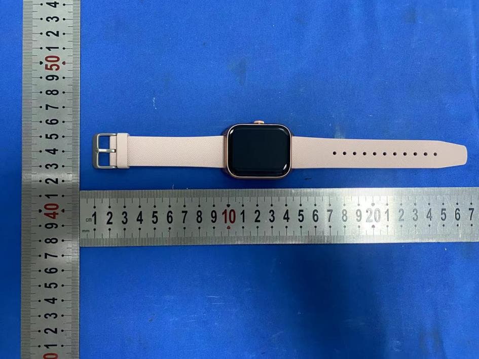
2A3D8-S2
Jun 23, 2024Qwatch
Equipment Class
DSS - Part 15 Spread Spectrum Transmitter