2A5EP-S10Tablet PC
SZ TPS CO., LTD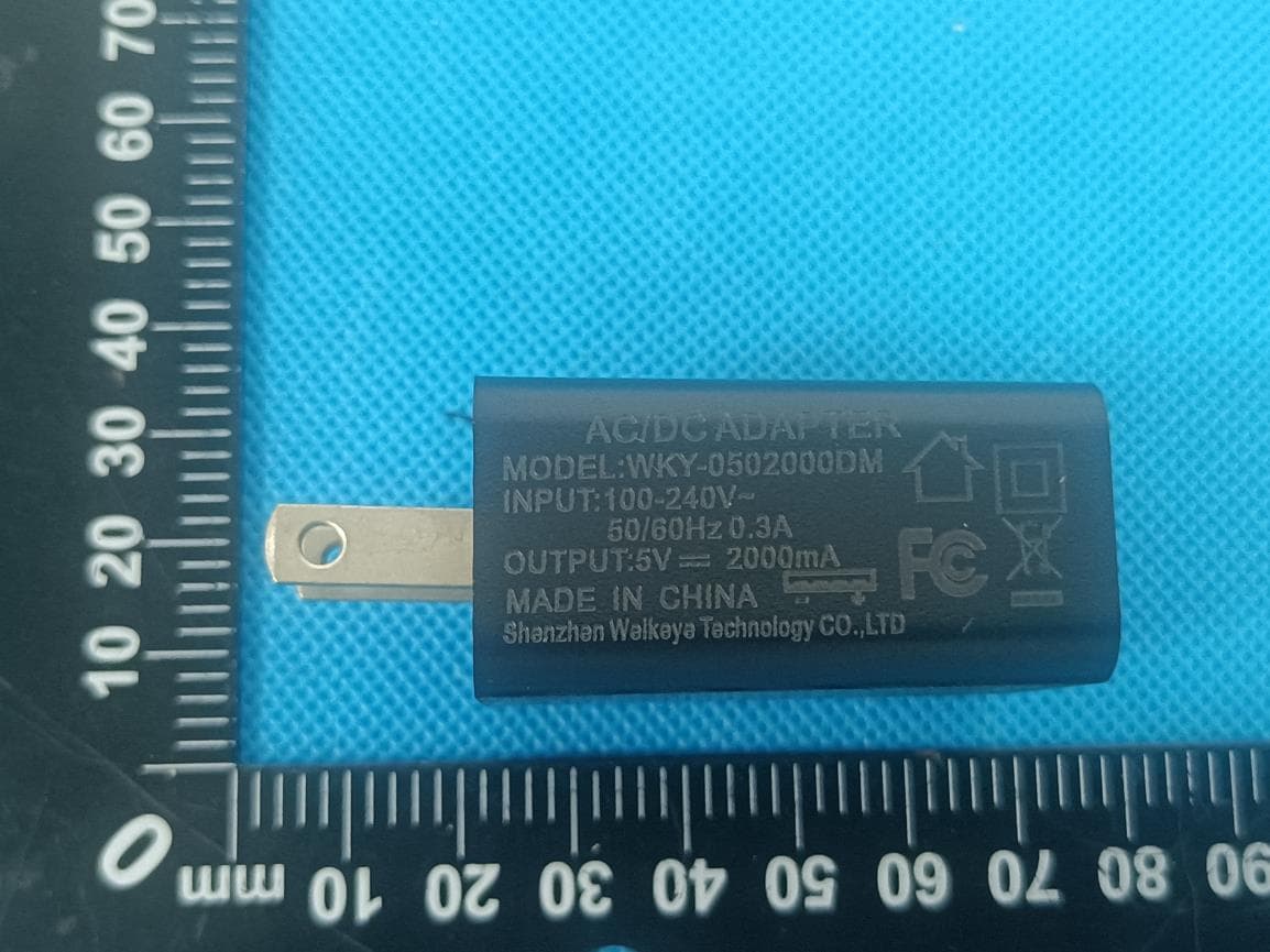
Click to zoom
Application Details
- Equipment Class
- DXX - Part 15 Low Power Communication Device Transmitter
- Date of Grant
- Apr 06, 2022
- Application Purpose
- Original Equipment
- Date of Application
- Apr 06, 2022
- Equipment Note
- Tablet PC
- Frequency Range
- 2402.00000000 - 2480.00000000
- Company
- SZ TPS CO., LTD
- Country
- China
Documents & Files
Document Text
Text extracted from the exhibit documents filed with the FCC. Open a document above to read the original.
Users Manual
User Manual Points for Attention 1. Do not use the player in exceptionally conditions:old or hot, dusty, damp or dry environments. 2. Do not allow the player to fall down while using it. 3. Please charge your battery when A. Battery power icon shows an empty icon; B. The system automatically shuts down and the power is soon off when you switch on the unit once again; C. There is no response if you operate on any key 4. Please do not disconnect power abruptly when the player is being formatted or in the process of uploading or downloading. Otherwise it may lead to the error in the program. 5. When this unit is used as a moving disk, the user shall store or export files in the proper file management operation method. Any improper operation method may lead to the loss of files, for which this Company will be held no liable. 6. Please do not dismantle this unit by yourself. If there is any inquiry, please contact the dealer. 7. There will be no separate notice in the case of any change in the functions and performance of this product. Basic Operation Power on In the shutdown state, long press "" button boots Power off In the power on state, long press the "" key 3 seconds then pop-up device options, select " Power off " for shut down. Sleep the machine under normal operating conditions, Short press the power button, Into hibernation, Now, Screen will close. Short press the power button again, Be able to resume normal mode. When the time being use this MID can enable this feature when, To reduce power consumption. Power reset If there is shutdown to the player in the process of operation, you can turn off and restart the player by pressing "reset" key. Screen time out If you do not contact the player within the set time, and do no operate by the button, the contact screen will be automatically turns off. In any state, short press "" button and for activation; Then skid the lock upwards to the green of spotted which will accomplish to access to the upper interface. If it is necessary to deactivate the contact screen time out function, you can set the [Screen time out] option under [display] function into "Never ". Using the Micro SD card After this unit is connected with the computer, you will find two moving disks. The first one is the built-in memory disk for this unit and the other is the disk for the Micro SD card. If no card is inserted, the second disk can not be opened. This unit supports the extension of the Micro SD card from 4GB to 64GB. Inserting and Pulling out the Micro SD card Inserting: Put the Micro SD card face up (side with words), and slightly force the card into the socket of the card, i.e. connecting the unit. Under this state, you can play the content in the Micro SD card. Pulling: Slightly push the Micro SD, and it will bounce by a section, and then you can take it out. Caution: Please perform inserting and pulling operation when power is off! Otherwise, it will lead to the loss or damage to the files within the unit! If no card is inserted, the computer will be unable to perform read and write operation for the disk notes of the later removable disk (Micro SD card). Battery: High capacity Polymer battery is used for this unit. The duration available of the battery power depends on volume, types of playing files and operation of batteries. The player can be set up by the user as "user define power off time" or "display setup" to save batteries. Charging: This unit can be recharged by USB port, you can also use DC Charger (when DC port is available). Take out the DC charger, plug it into the wall outlet with AC 220V(output current 1500mA,output voltage 5V~5.2V)), then plug in the DC jack into the device DC-in jack. Warnings for charging: 1. A new battery may be empty and not charged before you get the device. 2. If the device is not used for long time, it is better to charge it to full capacity every 2 or 3 months during storage. Power adapter is a key component of the portable player, which play a crucial role in keeping the portable player’s normal work and protecting your security when using the player, a long-term customer surveys and after-sales service Practice shows that the malfunction of the portable player In many cases were caused by using inappropriate accessories, in particular the power adapter. Use the substandard power adapter will shorten the life of the portable player by considerably, the voltage instability will seriously affected the normal work of the portable player and bring permanent damage on the player’s performance and reliability, Use the substandard power adapter will also reduced the vocal quality of the players, shutdown the player when you using it, In addition, Use the substandard power adapter will cause combustion and explosion which will disserve the safety of the consumers. Setting up your tablet 1. 2. After charging the battery, press and hold the power button for up to 5 seconds until the pattern is displayed. IMPORTANT: If the battery image is not displayed on the screen, press the power button briefly to display the image, and then press and hold the power button until the logo is displayed. 3.Follow the on-screen instructions to select a language and a wireless network. Lock and unlock Turn off the tablet Lock—Press the power button. Press and hold the power button, Unlock—Press the power button to touch Power off, and then touch OK. turn on the tablet, then place your If your tablet becomes unresponsive, finger on the lock icon and slide press and hold the power button for the icon to the unlock position several seconds to turn off the tablet. All apps—Displays a list of all apps installed. To confi you’re your preferences, touch , and then touch . Back—Opens the previous screen. Home—Opens or returns to the Home screen. Recent apps—Opens a list of apps used recently. NOTE: The appearance of the Home screen may vary. Search—Allows you to type one or more keywords to search. Voice search—Allows you to speak one or more keywords t…
Text truncated - open the document above for the full version.
Attestation Statements
SZ TPS CO., LTD Model Difference Product Name: Tablet PC Model Number: S10, S8-9863A, S7-7731E, Q8-7731E, S10-9863A, W116, P30, M70, M50, SF116, SF133, K116, Q7, Q8, Q10, SQ8, 7 inch Kids, N10, W133B, W101, P10, W801, K8, W102, FS8-6753, N4120, A789, RK3126 FCC Identifier: 2A5EP-S10 All the models are the same circuit and RF module, except the mode names and outlook color. Regards Sincerely Client’s signature Client’s name / title: Sam Fu / Manager Contact information: Floor 2, Building 2, No.596, Zhoushi Road, Jiuwei Community, Hangcheng Street, Baoan District, Shenzhen, China
Cover Letter(s)
SZ TPS CO., LTD 2022-03-23 Eurofins Electrical and Electronic Testing NA, Inc. 914 West Patapsco Avenue Baltimore, MD 21230 RE: CONFIDENTIALITY REQUEST FOR EUT NAME: Tablet PC MODEL : S8-9863A, S7-7731E, Q8-7731E, S10-9863A, W116, P30, M70, M50, SF116, SF133, K116, Q7, Q8, Q10, SQ8, 7 inch Kids, N10, W133B, W101, P10, W801, K8, W102, FS8-6753, N4120, A789, RK3126 FCC ID: 2A5EP-S10 To Whom It May Concern: This letter serves as an official request for confidentiality under sections 0.457 and 0.459 of CFR 47. We have requested that the - Block Diagram - Schematics - BOM - Tune Up Procedure - Operational Description - SOFTWARE SECURITY REQUIREMENTS FOR U-NII DEVICES required to be submitted with this application be permanently withheld from public review. The above materials contain trade secrets and proprietary information not customarily released to the public. The public disclosure of these materials may be harmful to the applicant and provide unjustified benefits to its competitors. Please contact me if there is any information you may need. Sincerely, Client’s name / title : Sam Fu / Manager Contact information / address: Floor 2, Building 2, No.596, Zhoushi Road, Jiuwei Community, Hangcheng Street, Baoan District, Shenzhen, China
ID Label/Location Info
Size:16*10mm MODEL: S10 FCC ID: 2A5EP-S10 Label location
Internal Photos
GSM,WCDMA, LTE Antenna BT,WIFI Antenna
Parts List/Tune Up Info
SN Component material number NamespecNo.Location 1PCB(MTK)K706/V1.0 (191.00*135.20)/4*1.0 FR41K706/V1.0 2131901000046chip resistor0Ω J(±5%) 0402 1/16W45 C209,C229,L609,L610,R1016,R103,R104,R1205,R1301,R1402 ,R1415,R201,R202,R205,R401,R418,R419,R421,R422,R511,R 513,R515,R518,R519,R520,R521,R522,R523,R531,R533,R535 ,R537,R539,R541,R543,R545,R546,R549,R551,R622,R623,R8 01,R803,R905,R906 3131901000120chip resistor0Ω J(±5%) 0603 1/10W2R101,R102 4131901000409chip resistor0.2Ω F(±1%) 0805 1/8W1R1403 5131901000505chip resistor5.1Ω F(±1%) 0402 1/16W1C1209 6131901000530chip resistor7.5Ω F(±1%) 0603 1/10W1R901 7131901000387chip resistor26.1Ω F(±1%) 0402 1/16W2R619,R621 8131901000074chip resistor27Ω J(±5%) 0402 1/16W1R502 9131901000388chip resistor35.7Ω F(±1%) 0402 1/16W1R620 10131901000478chip resistor36Ω F(±1%) 0402 1/16W1R308 11131901000001chip resistor100Ω F(±1%) 0402 1/16W2R407,R408 12131901000022chip resistor240Ω F(±1%) 0402 1/16W2R504,R505 13131901000028chip resistor470Ω F(±1%) 0402 1/16W2R402,R403 14131901000049chip resistor1K J(±5%) 0402 1/16W10R411,R415,R416,R425,R602,R604,R607,R608,R802,R1406 15131901000010chip resistor1.5K F(±1%) 0402 1/16W4R309,R409,R412,R417 16131901000285chip resistor2K F(±1%) 0402 1/16W1R615 17131901000083chip resistor3.3K J(±5%) 0402 1/16W1R1409 18131901000089chip resistor4.7K J(±5%) 0402 1/16W8R1110,R301,R302,R303,R304,R305,R306,R902 19131901000034chip resistor5.1K F(±1%) 0402 1/16W1R307 20131901000298chip resistor8.06K F(±1%) 0402 1/16W2R500,R501 21131901000003chip resistor10K F(±1%) 0402 1/16W2NTC301,R1417 22131901000050chip resistor10K J(±5%) 0402 1/16W5R1201,R1202,R1203,R1410,R612 23131901000302chip resistor16.9K F(±1%) 0402 1/16W1R1407 24131901000304chip resistor24K J(±5%) 0402 1/16W1R613 25131901000306chip resistor27K F(±1%) 0402 1/16W1R1408 26131901000027chip resistor39K F(±1%) 0402 1/16W2R1401,R331 27131901000090chip resistor47K J(±5%) 0402 1/16W3R423,R1418,R1419 28131901000736chip resistor75K F(±1%) 0402 1/16W1R1411 29131901000004chip resistor100K F(±1%) 0402 1/16W1R616 30131901000051chip resistor100K J(±5%) 0402 1/16W1R904 31131901000315chip resistor330K F(±1%) 0402 1/16W1R1405 32131901000091chip resistor470K J(±5%) 0402 1/16W1R420 33130101000002SMD capacitor1.8pF 0402 NPO C(±0.25pF) 50V1C231 34130101000007SMD capacitor4.7pF 0402 NPO C(±0.25pF) 50V1C225 35130101000013SMD capacitor18pF 0402 NPO J(±5%) 50V2C601,C226 36130101000014SMD capacitor22pF 0402 NPO J(±5%) 50V4C691,C693,C698,C699 37130101000016SMD capacitor33pF 0402 NPO J(±5%) 50V17 C401,C402,C405,C407,C408,C415,C419,C429,C430,C435,C43 7,C438,C440,C449,C450,C608,C6605 38130101000017SMD capacitor39pF 0402 NPO J(±5%) 50V1C609 39130101000019SMD capacitor56pF 0402 NPO J(±5%) 50V1C605 40130101000010SMD capacitor100pF 0402 NPO J(±5%) 50V10C202,C203,C211,C355,C431,C436,C439,C6603,C6606,C6607 41130101000040SMD capacitor220pF 0402 X7R K(±10%) 50V1C606 42130101000052SMD capacitor680pF 0402 X7R K(±10%) 50V1C227 43130101000445SMD capacitor0.1uF 0402 X5R M(±20%) 16V54 C101,C102,C103,C104,C105,C109,C110,C1109,C111,C1111,C 1112,C112,C113,C117,C118,C1201,C1203,C1206,C1207,C130 2,C1305,C1306,C201,C210,C213,C214,C215,C219,C221,C222 ,C418,C428,C501,C502,C504,C505,C506,C514,C515,C516,C5 17,C518,C527,C528,C607,C803,C810,C819,C821,C827,C828, C902,C903,C905 44130101000490SMD capacitor0.22uF 0402 Y5V Z(-20%~+80%) 16V4C216,C217,C223,C513 45130101000068SMD capacitor0.47uF 0402 Y5V Z(-20%~+80%) 10V5C218,C616,C617,C619,C620 46130101000449SMD capacitor1uF 0402 X5R K(±10%) 10V34 C106,C1110,C114,C120,C1202,C1208,C1303,C1304,C205,C20 6,C208,C212,C220,C228,C409,C410,C503,C524,C602,C615,C 618,C801,C804,C807,C808,C811,C814,C815,C820,C822,C824 ,C825,C826,C829 47130101000448SMD capacitor1uF 0402 X5R K(±10%) 25V2C805,C904 48130101000083SMD capacitor1uF 0603 Y5V Z(-20%~+80%) 25V1C1402 49130101000075SMD capacitor2.2uF 0603 Y5V Z(-20%~+80%) 10V5C521,C522,C523,C526,C802 50130101000526SMD capacitor4.7uF 0402 X5R M(±20%) 6.3V3C1205,C204,C207 51130101000332SMD capacitor4.7uF 0603 X5R M(±20%) 6.3V8C119,C525,C817,C901,C906,C907,C1107,C1301 52130101000025SMD capacitor10uF 0603 X5R M(±20%) 6.3V9C115,C432,C604,C689,C809,C812,C813,C908,C6604 53130101000419SMD capacitor22uF 0603 X5R M(±20%) 6.3V3C107,C116,C823 54130101000090SMD capacitor10uF 0805 Y5V Z(-20%~+80%) 16V2C1401,C1403 55130101000496SMD capacitor22uF 0805 Y5V M(±20%) 10V3C416,C417,C1405 56131301000085Chip Bead1.8K 85mA 0402 1.5Ω Murata3BEAD401,BEAD402,BEAD403 57131301000103Chip Bead220Ω 200mA 0603 0.3Ω TAI-TECH2BEAD406,BEAD408 58131301000002Chip Bead1000Ω 150mA 0603 0.7Ω1BEAD405 59131301000115Chip Bead2.5K 50mA 0603 1.4Ω TAI-TECH2BEAD416,BEAD417 60131102000297SMD ceramic inductors1.8nH 400mA S(±0.3nH) 0402 Sunlord1C695 61131102000015SMD ceramic inductors3.9nH 300mA S(±0.3nH) 0402 Sunlord1L608 62131102000380SMD ceramic inductors4.7nH 400mA S(±0.3nH) 0402 Sunlord1L203 63131102000096SMD ceramic inductors5.6nH 300mA S(±0.3nH) 0402 Sunlord2L603,L604 64131102000028SMD ceramic inductors6.2nH 300mA S(±0.3nH) 0402 Sunlord1C614 65131102000017SMD ceramic inductors8.2nH 300mA J(±5%) 0402 Sunlord1L202 66131102000034SMD ceramic inductors15nH 300mA J(±5%) 0402 Sunlord2L601,L602 67131102000367SMD ceramic inductors39nH 200mA J(±5%) 0402 Sunlord2C611,L606 68131107000170SMD Power Inductors0.68uH 2.2A N(±30%) 0.062Ω 2520102L801,L802 69131107000154SMD Power Inductors4.7uH 1.7A M(±20%) 0.09Ω 40181L1401 70130305000062SMD Schottky diode1N5819 1A 40V SOD-123 IET1C1406 71130302000019SMD zener diode5.1V 500mW SOD-123 LRC1D801 72131501000047SMD triodeNPN MMBT3904 (1AM/H1A) hFE=100-300 SOT23 HT2Q6,Q8 73131701000066SMD MOS P-channel SSC8013GS6 (1F9K) -3.8A -12V SOT-23 Spiritsemi 1Q7 74134802000067Patch SAW filter Diplexer DP1608-V1524CA 1500MHz/2400MHz 1.6*0.8*0.6mm ACX 1F201 75134802000078Patch SAW filter GPS SAW FAR-F6KA-1G5754-L4AJ GPS 1.4*1.0*0.5mm Taiyo-yuden 1U203 76134802000014Patch SAW filter Balun RFBLN2012090BM5T25 GSM850/900+GSM1800/1900 2.0*1.2,10Pinmm Walsin 1Z601 77132501000045SMD CLOCK26MHz ±0.5PPM 2.8V 25…
Text truncated - open the document above for the full version.
Test Report
Shenzhen DL Testing Technology Co., Ltd. Report No.: DL-20220321009-1E Test Report Tel: 400-688-3552 Web:www.dl-cert.com Email: [email protected] Page 1 of 40 FCC Part 15C Test Report FCC ID: 2A5EP-S10 Applicant: SZ TPS CO., LTD Address: Floor 2, Building 2, No.596, Zhoushi Road, Jiuwei Community, Hangcheng Street, Baoan District, Shenzhen, China Manufacturer: SZ TPS CO., LTD Address: Floor 2, Building 2, No.596, Zhoushi Road, Jiuwei Community, Hangcheng Street, Baoan District, Shenzhen, China EUT: Tablet PC Trade Mark: N/A Model Number: S10, S8-9863A, S7-7731E, Q8-7731E, S10-9863A, W116, P30, M70, M50, SF116, SF133, K116, Q7, Q8, Q10, SQ8, 7 inch Kids, N10, W133B, W101, P10, W801, K8, W102, FS8-6753, N4120, A789, RK3126 Date of Receipt: Feb. 25, 2022 Test Date: Feb. 25, 2022 – Mar. 20, 2022 Date of Report: Mar. 20, 2022 Prepared By: Shenzhen DL Testing Technology Co., Ltd. Address: 101-201, Building C, Shuanghuan, No.8, Baoqing Road, Baolong Industrial Zone, Baolong Street, Longgang District, Shenzhen, Guangdong, China Applicable Standards: FCC PART 15 C 15.249 ANSI C63.10:2013 Test Result: Pass Report Number: DL-20220321009-1E Prepared (Test Engineer): Pxing Huang Reviewer (Supervisor): Jack Bu Approved (Manager): Jade Yang This test report is based on a single evaluation of one sample of above mentioned products. It is not permitted to be duplicated in extracts without written approval of Shenzhen DL Testing Technology Co., Ltd. Shenzhen DL Testing Technology Co., Ltd. Report No.: DL-20220321009-1E Test Report Tel: 400-688-3552 Web:www.dl-cert.com Email: [email protected] Page 2 of 40 Table of Contents Page 1 . SUMMARY OF TEST RESULTS 4 1.1 MEASUREMENT UNCERTAINTY 4 2 . GENERAL INFORMATION 5 2.1 GENERAL DESCRIPTION OF EUT 5 2.2 DESCRIPTION OF TEST MODES 6 2.3 BLOCK DIGRAM SHOWING THE CONFIGURATION OF SYSTEM TESTED 7 2.4 DESCRIPTION OF SUPPORT UNITS(CONDUCTED MODE) 7 2.5 TABLE OF PARAMETERS OF TEST SOFTWARE SETTING 7 2.6 EQUIPMENTS LIST FOR ALL TEST ITEMS 8 3 . EMC EMISSION TEST 9 3.1 CONDUCTED EMISSION MEASUREMENT 9 3.1.1 POWER LINE CONDUCTED EMISSION LIMITS 9 3.1.2 TEST PROCEDURE 9 3.1.3 DEVIATION FROM TEST STANDARD 9 3.1.4 TEST SETUP 10 3.1.5 EUT OPERATING CONDITIONS 10 3.1.6 TEST RESULTS 10 3.2 RADIATED EMISSION MEASUREMENT 13 3.2.1 RADIATED EMISSION LIMITS 13 3.2.2 TEST PROCEDURE 14 3.2.3 DEVIATION FROM TEST STANDARD 14 3.2.4 TEST SETUP 14 3.2.5 EUT OPERATING CONDITIONS 15 3.2.6 TEST RESULTS (BETWEEN 9KHZ – 30 MHZ) 16 3.2.7 TEST RESULTS (BETWEEN 30MHZ – 1GHZ) 17 3.2.8 TEST RESULTS (1GHZ~25GHZ) 19 3.3 RADIATED BAND EMISSION MEASUREMENT 22 3.3.1 TEST REQUIREMENT: 22 3.3.2 TEST PROCEDURE 22 3.3.3 DEVIATION FROM TEST STANDARD 22 3.3.4 TEST SETUP 23 3.3.5 EUT OPERATING CONDITIONS 23 4 . BANDWIDTH TEST 28 4.1 APPLIED PROCEDURES / LIMIT 28 4.1.1 TEST PROCEDURE 28 4.1.2 DEVIATION FROM STANDARD 28 4.1.3 TEST SETUP 28 Shenzhen DL Testing Technology Co., Ltd. Report No.: DL-20220321009-1E Test Report Tel: 400-688-3552 Web:www.dl-cert.com Email: [email protected] Page 3 of 40 Table of Contents Page 4.1.4 EUT OPERATION CONDITIONS 28 4.1.5 TEST RESULTS 29 5 . ANTENNA REQUIREMENT 35 5.1 STANDARD REQUIREMENT 35 5.2 EUT ANTENNA 35 6 . TEST SEUUP PHOTO 36 7 . EUT PHOTO 38 Shenzhen DL Testing Technology Co., Ltd. Report No.: DL-20220321009-1E Test Report Tel: 400-688-3552 Web:www.dl-cert.com Email: [email protected] Page 4 of 40 1. SUMMARY OF TEST RESULTS Test procedures according to the technical standards: FCC Part15 (15.249) , Subpart C Standard Section Test Item Judgment Remark 15.207 Conducted Emission PASS 15.249(c) Fundamental &Radiated Spurious Emission Measurement PASS 15.205 Band Edge Emission PASS 15.215 20dB Bandwidth PASS 15.203 Antenna Requirement PASS NOTE: (1)” N/A” denotes test is not applicable in this Test Report 1.1 MEASUREMENT UNCERTAINTY The reported uncertainty of measurement y ± U, where expended uncertainty U is based on a standard uncertainty multiplied by a coverage factor of k=2,providing a level of confidence of approximately 95 %. No. Item Uncertainty 1 Conducted Emission Test ±2.56dB 2 RF power,conducted ±0.42dB 3 Spurious emissions,conducted ±2.76dB 4 All emissions,radiated(<1G) ±3.65dB 5 All emissions,radiated(>1G) ±4.89dB 6 Temperature ±0.5°C 7 Humidity ±2% Shenzhen DL Testing Technology Co., Ltd. Report No.: DL-20220321009-1E Test Report Tel: 400-688-3552 Web:www.dl-cert.com Email: [email protected] Page 5 of 40 2. GENERAL INFORMATION 2.1 GENERAL DESCRIPTION OF EUT Product Name: Tablet PC Trademark N/A Model No.: S10 S8-9863A, S7-7731E, Q8-7731E, S10-9863A, W116, P30, M70, M50, SF116, SF133, K116, Q7, Q8, Q10, SQ8, 7 inch Kids, N10, W133B, W101, P10, W801, K8, W102, FS8-6753, N4120, A789, RK3126 Model Difference All samples are the same except the model number and appearance color, so we prepare " S10" for test only. Operation Frequency: 2402~2480MHz Channel numbers: 79 Channels Transfer Rate: 1/2/3Mbps Channel separation 1MHz Modulation technology: GFSK, PI/4 DQPSK, 8DPSK Antenna Type: Internal Antenna Antenna gain: 2dBi Power supply: DC 3.7V from battery DC 5V from Charger Charger Model:WKY-0502000DM Input: AC 100-240V 50/60Hz 0.3A Output: DC 5V 2000mA Note: 1.For a more detailed features description, please refer to the manufacturer’s specifications or the User's Manual. 2.The EUT’s all information provided by client. Shenzhen DL Testing Technology Co., Ltd. Report No.: DL-20220321009-1E Test Report Tel: 400-688-3552 Web:www.dl-cert.com Email: [email protected] Page 6 of 40 3. Channel List Channel Frequency (MHz) Channel Frequency (MHz) Channel Frequency (MHz) 00 2402 27 2429 54 2456 01 2403 28 2430 55 2457 02 2404 29 2431 56 2458 03 2405 30 2432 57 2459 04 2406 31 2433 58 2460 05 2407 32 2434 59 2461 06 2408 33 2435 60 2462 07 2409 34 2436 61 2463 08 2410 35 2437 62 2464 09 2411 36 2438 63 2465 10 2412 37 2439 64 2466 11 2413 38 2440 65 2467 12 2414 39 2441 66 2468 13 2415 40 2442 67 2469 14 2416 41 2443 68 2470 15 2417 42 2444 69 2471 16 2418 43 24…
Text truncated - open the document above for the full version.
Test Setup Photos
Radiated Measurement Photos Conducted Measurement Photos
Contact Information
Applicant
Sam Fu
Technical Contact
Shenzhen DL Testing Technology Co., Ltd.Jade Yang
[email protected]+864006883552
101-201, Building C, Shuanghuan, No.8,Baoqing Road · Shenzhen · China
Test Firm
Shenzhen DL Testing Technology Co., Ltd.Jade Yang
[email protected]400-688-3552
Technical Specifications
| # | Rule Parts | Frequency Range | Power Output |
|---|---|---|---|
| 1 | 15C | 2.40 GHz - 2.48 GHz | - |