2A5NH-CBLC9LED lamp
Ningbo Klite Electric Manufacture Co., Ltd.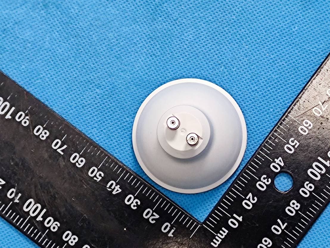
Click to zoom
Application Details
- Equipment Class
- DTS - Digital Transmission System
- Date of Grant
- Dec 05, 2022
- Application Purpose
- Original Equipment
- Date of Application
- Dec 05, 2022
- Equipment Note
- LED lamp
- Frequency Range
- 2402.00000000 - 2480.00000000
- Country
- China
Documents & Files
Document Text
Text extracted from the exhibit documents filed with the FCC. Open a document above to read the original.
Users Manual
LED Lamp LED Lamp FCCWARINGAny Changes expressly or modifications not approved by the part y responsible for compliance couldvoid the user's authority to operate the equipment. This device complies with part 15 of the FCC Rules. Operation i s subject to the following two conditions:(1) This device may n ot cause harmful interference,and (2) this device must accept any interference r eceived, including interference that may causeundesired operati on. FCC Radiation Exposure Statement:This equipment complies with FCC radiation exposure limits set forth for an uncontrolled environment . This transmitter must not be co located or operating in conjunction with any other antenna or t ransmitter. This equipment should be installed and operated with minimum di stance 20cm between the radiator &you body. Note: This equipment has been tested and found to comply with t he limits for a Class B digital device,pursuant to part 15 of t he FCC Rules. These limits are designed to provide reasonable protection against harmful inter ference in a residential installation. This equipment generates , uses and can radiate radio frequency energy and, if not installed and used in accordance w ith the instructions, may cause harmful interference to radio c ommunications. However, there is no guarantee that interference will not occur in a particular i nstallation. If this equipment does cause harmful interference to radio or television reception, which can be determined by turning the equipment off and on, the user is encouraged to try to correct the interference by one or mor e of the following measures: —Reorient or relocate the receiving antenna.—Increase the separation between the equipment and receiver.—Connect the equipment into an outlet on a circuit different fr om that to which the receiver is connected.—Consult the dealer or an experienced radio/TV technician for h elp.
Cover Letter(s)
Applicant name: Ningbo Klite Electric Manufacture Co., Ltd. ADD: No.5 Dapuhe Road, Beilun, Ningbo, 315800 Zhejiang, China Telephone No.: 0574-55846043 E-mail: [email protected] DECLARATION OF SIMILARITY Date: 2022-10-12 FEDERAL COMMUNICATIONS COMMISSION Authorization and Evaluation Division 7435 Oakland Mills Road Columbia, MD 21046 Dear Sir or Madam: We, Ningbo Klite Electric Manufacture Co., Ltd., hereby declare that the product: LED Lamp, FCC ID:2A5NH-CBLC9. model: GU10-2B WI FI+BLE TR 4.9W GU10 X-Y are electrically identical with the PCB design, components and electromagnetic compatibility characteristics, and mo del: GU10-2B WIFI+BLE TR 4.9W GU10 2700K-6500K has been tested by China Certification ICT Co., Ltd (Dongguan). A description of the differences between those models and that are declared similar are as follows: The Testing Model The Multiple Model Different ItemThe Different Details GU10‐2B WIFI+BLE TR 4.9W GU10 2700K‐6500K GU10‐2B WIFI+BLE TR 4.9W GU10 X‐Y CCT The difference between the testing model and multiple model is CCT and Envelope Finish; “X”&“Y” represents the CCT, it can be1800K、2200K、2700K、3000K、3500K、 4000K、4500K、5000K、5700K、6500K, but X≠Y; Please contact me should there be need for any additional clarification or information. Best Regards, Signature: Printed Name: Xueni Jia Title: Certification director
External Photos
EXHIBIT B - EUT EXTERNAL PHOTOGRAPHS EUT
Internal Photos
EXHIBIT C - EUT INTERNAL PHOTOGRAPHS Uncover Chip Chip Antenna
RF Exposure Info
China Certification ICT Co., Ltd (Dongguan) Report No.: CR220941631-00B Page 62 of 62 5. RF EXPOSURE EVALUATION 5.1 Applicable Standard FCC §15.247 (i) Systems operating under the provisions of this section shall be operated in a manner that ensures that the public is not exposed to radio frequency energy levels in excess of the Commission's guidelines. See §1.1307(b)(1) of this chapter. 5.2 Procedure According to §1.1307(b)(3)(i) (C) Or using Table 1 and the minimum separation distance (R in meters) from the body of a nearby person for the frequency (f in MHz) at which the source operates, the ERP (watts) is no more than the calculated value prescribed for that frequency. For the exemption in Table 1 to apply, R must be at least λ/2π, where λ is the free-space operating wavelength in meters. If the ERP of a single RF source is not easily obtained, then the available maximum time-averaged power may be used in lieu of ERP if the physical dimensions of the radiating structure(s) do not exceed the electrical length of λ/4 or if the antenna gain is less than that of a half-wave dipole (1.64 linear value). Table 1 to § 1.1307(b)(3)(i)(C) - Single RF Sources Subject to Routine Environmental Evaluation RF Source frequency (MHz) Threshold ERP (watts) 0.3-1.34 1,920 R 2 . 1.34-30 3,450 R 2 /f 2 . 30-300 3.83 R 2 . 300-1,500 0.0128 R 2 f. 1,500-100,000 19.2R 2 . 5.3 Measurement Result Radio Frequency (MHz) λ/2 Π (mm) Distance (mm) Exemption ERP (mW) Maximum Conducted Power including Tune-up Tolerance (dBm) Antenna Gain (dBi) ERP MPE- Based Exemption dBm mW WiFi 2412-2462 19.80 200 768 14 4.75 16.60 45.71 Compliant BLE 2402-2480 19.88 200 768 3 4.75 5.60 3.63 Compliant Note: The Value of Maximum Conducted Power including Tune-up Tolerance was declared by the customer. Result: The device compliant the MPE-Based Exemption at 20cm distances. ===== END OF REPORT ====
Test Report
TEST REPORT Applicant: Ningbo Klite Electric Manufacture Co., Ltd. Address: No.5 Dapuhe Road, Beilun, Ningbo, 315800 Zhejiang, China FCC ID: 2A5NH-CBLC9 Product Name: LED lamp Standard(s): 47 CFR Part 15, Subpart C(15.247) ANSI C63.10-2013 KDB 558074 D01 15.247 Meas Guidance v05r02 The above equipment has been tested and found compliant with the requirement of the relative standards by China Certification ICT Co., Ltd (Dongguan) Report Number: CR220941631-00B Date Of Issue: 2022-10-04 Reviewed By: Sun Zhong Title: Manager Test Laboratory: China Certification ICT Co., Ltd (Dongguan) No. 113, Pingkang Road, Dalang Town, Dongguan, Guangdong, China Tel: +86-769-82016888 China Certification ICT Co., Ltd (Dongguan) Report No.: CR220941631-00B Page 2 of 62 Test Facility The Test site used by China Certification ICT Co., Ltd (Dongguan) to collect test data is located on the No. 113, Pingkang Road, Dalang Town, Dongguan, Guangdong, China. The lab has been recognized as the FCC accredited lab under the KDB 974614 D01 and is listed in the FCC Public Access Link (PAL) database, FCC Registration No. : 442868, the FCC Designation No. : CN1314. The lab has been recognized by Innovation, Science and Economic Development Canada to test to Canadian radio equipment requirements, the CAB identifier: CN0123. Declarations China Certification ICT Co., Ltd (Dongguan) is not responsible for the authenticity of any test data provided by the applicant. Data included from the applicant that may affect test results are marked with a triangle symbol “▲”. Customer model name, addresses, names, trademarks etc. are not considered data. Unless otherwise stated the results shown in this test report refer only to the sample(s) tested. This report cannot be reproduced except in full, without prior written approval of the Company. This report is valid only with a valid digital signature. The digital signature may be available only under the Adobe software above version 7.0. This report may contain data that are not covered by the accreditation scope and shall be marked with an asterisk “★”. China Certification ICT Co., Ltd (Dongguan) Report No.: CR220941631-00B Page 3 of 62 CONTENTS T EST FACILITY .......................................................................................................................................... 2 DECLARATIONS .......................................................................................................................................... 2 1. GENERAL INFORMATION .................................................................................................... 5 1.1 PRODUCT DESCRIPTION FOR EQUIPMENT UNDER TEST (EUT) ....................................................... 5 1.2 DESCRIPTION OF TEST CONFIGURATION ........................................................................................... 7 1.2.2 Support Equipment List and Details .............................................................................................................. 7 1.2.3 Support Cable List and Details ...................................................................................................................... 7 1.2.4 Block Diagram of Test Setup ......................................................................................................................... 8 1.3 MEASUREMENT UNCERTAINTY .......................................................................................................... 9 2. SUMMARY OF TEST RESULTS .......................................................................................... 10 3. REQUIREMENTS AND TEST PROCEDURES .................................................................. 11 3.1 AC LINE CONDUCTED EMISSIONS .................................................................................................... 11 3.1.1 Applicable Standard ..................................................................................................................................... 11 3.1.2 EUT Setup.................................................................................................................................................... 12 3.1.3 EMI Test Receiver Setup ............................................................................................................................. 12 3.1.4 Test Procedure ............................................................................................................................................. 13 3.1.5 Corrected Amplitude & Margin Calculation ................................................................................................ 13 3.2 RADIATION SPURIOUS EMISSIONS .................................................................................................... 14 3.2.1 Applicable Standard ..................................................................................................................................... 14 3.2.2 EUT Setup.................................................................................................................................................... 14 3.2.3 EMI Test Receiver & Spectrum Analyzer Setup ......................................................................................... 15 3.2.4 Test Procedure ............................................................................................................................................. 15 3.2.5 Corrected Amplitude & Margin Calculation ................................................................................................ 15 3.3 6 DB EMISSION BANDWIDTH: ............................................................................................................ 16 3.3.1 Applicable Standard ..................................................................................................................................... 16 3.3.2 EUT Setup.........................................................................................................................…
Text truncated - open the document above for the full version.
Test Report
嘉兴佳利电子有限公司http://www.glead.com.cn阿里巴巴http://zydq.en.alibaba.com JIAXINGGLEADELECTRONICSCO.,LTD -1- 产品技术规格书 SPECIFICATION 中国浙江省嘉兴市经济开发区正原路66号 No.66ZhengyuanRoad,EconomicDevelopmentZone,Jiaxing,Zhejiang,China TEL:0086-573-83651818FAX:0086-573-83651858 拟制 Preparedby :审核 Checkedby :批准 Approvedby : 送样日期 FormedOn 产品版本 DocumentVersion (V1.1) 产品型号PARTNO:LA31H2450-A55 客户料号CUSTOMERPARTNO: 客户确认CUSTOMERAPPROVEDBY: 确认日期APPROVEDDATE: 嘉兴佳利电子有限公司http://www.glead.com.cn阿里巴巴http://zydq.en.alibaba.com JIAXINGGLEADELECTRONICSCO.,LTD -2- 目录 Tableofcontents 规格书版本更改记录Versionrejiggertrackrecord..............................3 1.概述Introduction..................................................................4 2.型号PartNumber...............................................................4 3.外型尺寸及测试板焊盘尺寸Dimensions.....................4~5 4.测试电路和匹配电路EvaluationBoardandMatchingCircuits............5 5.电气性能ElectricalCharacteristics..........................................6 6.特性曲线Characteristiccurve...................................................6 7.方向图RadiationPattern...................................................7~8 8.可靠性试验后允许误差PostDependabilityTolerance...............9 9.可靠性试验DependabilityTest..........................................9~10 10.回流焊温度ReflowSolderingStandardCondition.....................10 11.包装尺寸PackagingandDimensions....................................11 嘉兴佳利电子有限公司http://www.glead.com.cn阿里巴巴http://zydq.en.alibaba.com JIAXINGGLEADELECTRONICSCO.,LTD -3- 产品规格书版本更改记录 Versionrejiggertrackrecord 版本号 Version 更改记录Rejigger 拟制 Prepared 批准 Approve 日期 Date V1.0首次发行潘枫卢冠宇2018.12.07 V1.1 修改第三点外形尺寸A公差为 0.4+0.1/-0.2mm 潘枫卢冠宇2020.08.18 备注: 1、更改产品电性能指标时,版本号需更换(V1.0换为V2.0、V3.0......); 2、更改产品测试方法(包括可靠性测试条件),或更改使用条件时,当前版本号加系列(V1.0 换为V1.1、V1.2......)。 嘉兴佳利电子有限公司http://www.glead.com.cn阿里巴巴http://zydq.en.alibaba.com JIAXINGGLEADELECTRONICSCO.,LTD -4- 产品尺寸/Size:3.2×1.6×0.6 1.概述 INTRODUCTION " 佳利 " 微波多层陶瓷天线 LA 系列产品设计用于 WLAN 、 WiFi 、蓝牙、 PHS ,手机 多频天线 ,FM 等小体积 SMD 片式设计。 "GLEAD"MicrowaveMulti-LayerCeramicAntennaLAseriesaredesignedtobeused inWLAN 、 WiFi 、 Bluetooth 、 PHS 、 Multiple-bandMobilephoneantenna,FM,etcand compactsizeSMDchipdesign. 2.型号 PartNumber LA31H2450-A55 3.外型尺寸 Dimensions ( Unit : mm ) NumberTerminalName ①INPUT ②NC SymbolsLWTA Dimensions3.2+/-0.21.6+/-0.20.6+/-0.10.4+0.1/-0.2 天线频率/AntennaFrequency:2450MHz 产品设计结构H型/ViaDesignSeries 多层结构天线/Multi-layerAntenna 产品名称,编号A55/ProductName:A55 (TopView) L w ①② (BottomView) A (SideView) T 嘉兴佳利电子有限公司http://www.glead.com.cn阿里巴巴http://zydq.en.alibaba.com JIAXINGGLEADELECTRONICSCO.,LTD -5- 4.测试电路和匹配电路EvaluationBoardandMatchingCircuits 5.1nH 1.5pF 嘉兴佳利电子有限公司http://www.glead.com.cn阿里巴巴http://zydq.en.alibaba.com JIAXINGGLEADELECTRONICSCO.,LTD -6- 5.电气性能ElectricalCharacteristics 6.特性曲线 Characteristiccurve No. Item(项目)Specifications(特性) 5.1(带匹配电路测试)AfterMatching2450MHz 5.2BandWidth通带宽度100MHztyp. 5.3PeakGain峰值增益4.75dBi 5.4V.S.W.R驻波比≤2.0 5.5 Polarization极化方式 Linear线性 5.6 AzimuthBeamwidth方位角 Omni-directional全向 5.7 Impedance阻抗 50Ω 嘉兴佳利电子有限公司http://www.glead.com.cn阿里巴巴http://zydq.en.alibaba.com JIAXINGGLEADELECTRONICSCO.,LTD -7- 7. 方向图 RadiationPattern coordinates: X-ZPlane Y-ZPlane X-Y Plane 嘉兴佳利电子有限公司http://www.glead.com.cn阿里巴巴http://zydq.en.alibaba.com JIAXINGGLEADELECTRONICSCO.,LTD -8- 3DRadiationPattern Frequency (MHz) 240024502500 Avg.Gain (dBi) -2.25-2.23-2.25 PeckGain (dBi) 3.684.753.72 Efficiency (%) 687169 嘉兴佳利电子有限公司http://www.glead.com.cn阿里巴巴http://zydq.en.alibaba.com JIAXINGGLEADELECTRONICSCO.,LTD -9- 8可靠性试验后允许误差PostDependabilityTolerance 经可靠性试验后允许比起始读数偏差见下表 PostDependabilityTolerance(Refertothetable) 9可靠性试验DependabilityTest 基准条件:温度范围Temperaturerange25±5°C 相对湿度范围RelativeHumidityrange55~75%RH 工作温度OperatingTemperaturerange-40°C~+85°C 9.1耐振动VibrationResist 在振动频率为10~55Hz振幅为1.5mm沿X.Y.Z方向各振动2小时后测试符合表8.1~8.4规定。 Thedeviceshouldsatisfytheelectricalcharacteristicsspecifiedinparagraph8.1~8.4afterappliedto thevibrationof10to55Hzwithamplitudeof1.5mmfor2hourseachinX,YandZdirections. 9.2耐跌落冲击DropShock 在100cm高度处按X,Y,Z三个面分别自由跌落在木制地板上共3次后测试符合表8.1~8.4规 定。 Thedeviceshouldsatisfytheelectricalcharacteristicsspecifiedinparagraph8.1~8.4afterdropping ontothehardwoodenboardfromtheheightof100cmfor3timeseachfacetofthe3dimensionsofthe device. 9.3耐焊接热SolderHeatProof 能承受经120~150°C的温度预热120秒后,在255°C+10°C的焊锡浸5±0.5秒,或300°C-10°C的 电烙铁焊接3±0.5秒,焊接面无损伤。 Thedeviceshouldbesatisfiedafterpreheatingat120°C~150°Cfor120secondsanddippingin solderingSnat255°C+10°Cfor5±0.5seconds,orelectriciron300°C-10°Cfor3±0.5seconds, withoutdamnify. 9.4推力试验AdhesiveStrengthofTermination 在产品电极端子上或表面上可承受5N(≦0603);10N(>0603)水平推力10±1秒而无明显外观损坏 与电极移位。 Thedevicehavenoremarkabledamageorremovaloftheterminationafterhorizontalforceof 5N(≦0603);10N(>0603)with10±1seconds. No.Item(项目) PostDependabilityTolerance (可靠性试验后允许附加误差) 8.1CentralFrequency中心频率±5MHz 8.2BandWidth通带宽度±5MHz 8.3Gain增益±0.1dBi 8.4V.S.W.R(inBW)驻波比±0.1 嘉兴佳利电子有限公司http://www.glead.com.cn阿里巴巴http://zydq.en.alibaba.com JIAXINGGLEADELECTRONICSCO.,LTD -10- 9.5耐弯曲试验BendingResistTest 将产品按图焊在1.6±0.2mm的PCB板中间,由箭头方向施 力:1mm/S,弯曲距离:1.5mm,保持5±1S,产品金属层无脱落。 WeldtheproducttothecenterpartofthePCBwiththethickness 1.6±0.2mmastheillustrationshows,andkeepexertingforce arrow-wardonitatspeedof:1mm/S,andholdfor5±1Satthe positionof1.5mmbendingdistance,sofar,anypeelingoffofthe productmetalcoatingshouldnotbedetected. 9.6耐湿热特性MoistureProof 在温度为60±2°C,相对湿度90~95%的恒温湿箱中放置96小时,在常温中恢复1~2小时后测 试,符合表8.1~8.4规定。 Thedeviceshouldsatisfytheelectricalcharacteristicsspecifiedinparagraph8.1~8.4afterexposedto thetemperature60±2°Candtherelativehumidity90~95%RHfor96hoursand1~2hoursrecoverytime undernormalcondition. 9.7高温特性HighTemperatureEndurance 在温度为85±5°C的恒温箱中放置96±2小时,在常温中恢复1~2小时后测试。符合表8.1~8.4 规定。 Thedeviceshouldsatisfytheelectricalcharacteristicsspecifiedinparagraph8.1~8.4afterexposedto temperature85±5°Cfor96±2hoursand1~2hoursrecoverytimeundernormaltemperature. 9.8低温特性LowTemperatureEndurance 在温度为-40°C±5°C低温箱中放置96±2小时后恢复1~2小时测试符合表8.1~8.4规定。 Thedeviceshouldalsosatisfytheelectricalcharacteristicsspecifiedinparagraph8.1~8.4afterexposed tothe…
Text truncated - open the document above for the full version.
Test Setup Photos
EXHIBIT D - TEST SETUP PHOTOGRAPHS Conducted Emissions Front View Conducted Emissions Side View Radiated Emission Below 1GHz View Radiated Emission Above 1GHz View
Contact Information
Applicant
Xueni Jia(Certification Director)
Test Firm
CHINA CERTIFICATION ICT CO., LTD (DONGGUAN)Tanie Ou
[email protected]0086 0769 86858888
Technical Specifications
| # | Rule Parts | Frequency Range | Power Output |
|---|---|---|---|
| 2 | 15C | 2.40 GHz - 2.48 GHz | 2.00 mW |