2A6ZN-P200Industrial Photocurable 3D Printer
Suzhou Laisai Intelligence Technology Co.,Ltd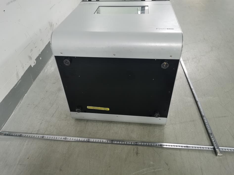
Click to zoom
Application Details
- Equipment Class
- DTS - Digital Transmission System
- Date of Grant
- Nov 06, 2022
- Application Purpose
- Original Equipment
- Date of Application
- Nov 06, 2022
- Equipment Note
- Industrial Photocurable 3D Printer
- Frequency Range
- 2412.00000000 - 2462.00000000
- Country
- China
Documents & Files
Document Text
Text extracted from the exhibit documents filed with the FCC. Open a document above to read the original.
Users Manual
P200 Series User Manual V1.0 2 Contents General Information 1 Information 2 Safety Guidelines 3 Product Information 5 Technical Specification 6 Technical Principle 7 Installation and Debugging 8 Installation Requirement 9 Unpacking 10 Equipment 12 Installation 13 Interface Introduction 18 Printing 25 Post-Processing 28 Maintenance 32 Troubleshooting 34 Warranty 36 Warranty 37 Technical Support 38 Contact 39 Warranty Card 40 1 General Information 2 Information Instructions This manual contains technical information, safety guidelines, and detailed operation instructions for P200 series DLP 3D printers. Please read this manual carefully before using the device. Failure to comply with the safety and operating instructions required by this manual will result in consequences for the user's responsibility. All information contained in this manual is up to date at printing, but may be subject to change without notice when product is upgraded. The images used in this manual may differ from your device due to differences in specific models and specifications. ©2021 Suzhou Laisai Technology Co., Ltd. All rights reserved. Instructions of mark Warning : This could result in serious personal injury or equipment damage if it was failed to comply with this requirement. Attention : This could result in minor personal injury or equipment damage if it was failed to comply with this requirement. Important Information : The normal operation of the device or the quality of printed products would be influenced if it was failed to comply with this requirement. Protection requirements : The precautions should be taken as required. Hazard indication : Description of specified hazard. UV 3 UV Safety Guidelines Before operating with the printer, please read the following safety guidelines to identify the potential risks which you may experience during the usage. Then make sure to comply with the related requirement defined in the manual and take appropriate precautions during operation. Any operation that fails to fulfill with the safety guidelines may result in personal injury or equipment damage, and the users themselves should finally take the corresponding consequences. The device shall be operated by professional staff Keep away from children Disassembly or modification is strictly prohibited It is strictly prohibited to disassemble or modify the device without authorization. In addition, do not use accessories that are not designated by RAYSHAPE officially. Please keep the device, resin material and other accessories out of the reach of children. Operators must carefully read and understand the safety guide and operation manual, then operate with the device correctly as required. Risk of UV exposure When the printer and post-curing device are working, please keep protective cover / door closed normally. If any operation or maintenance work should be proceeded while the device is working, the anti-UV goggles shall be worn accordingly. The specification of power must meet the operating requirements of the device. A grounded electrical outlet should be used. If the power cable is found aging or damaged, replace it before using the device. Risk of electric shock Both the printer and post-curing device are designed basing on the principle of UV light curing, and there is UV light available inside the device during operation, the risk of UV light exposure shall be avoided accordingly. 4 Safety Guidelines Risk of mechanical extrusion The printing platform will move up and down while the printer is working, there is a risk of mechanical extrusion generated by the improper operation. Wear protective gloves Good ventilation Risk of sharp edge cutting After printing, a shovel blade is used to separate the printed parts from the printing platform. There is a risk of getting injured by the sharp edge cutting of the shovel blade. Risk of flammability of cleaning solvent The printed parts should be cleaned with a cleaning solvent, such as IPA or 95% alcohol. Wear goggles Please keep the protective cover/door normally closed when the printer is in service. It is strictly forbidden to put hands or other parts of the body into the printing area during the printing. Anti-cutting gloves should be worn during the operation of separating printed parts from the platform. The shovel’s blade should not be orientated to your body during the usage. Please keep good ventilation and keep away from heat and fire sources when storing or using cleaning solvent. When operating the devices, please wear disposable gloves to avoid direct contact with the resin material. When removing the printed parts from printing platform with a shovel, please wear cut- resistant gloves Areas for printer installation and post-processing should be well ventilated. If any operation or maintenance work is needed to proceed while the printer is working, anti-UV goggles should be worn accordingly. Goggles should be worn to avoid the injury caused by the splashing fragment when separating printed parts from printing platform. Risk of scalding The printer is equipped with a heater. Please avoid scalding if the heater is on. 5 Product Information 6 Specification P200P200 HDP200 UHD Build volume144 × 81 × 190 mm96 × 54 × 190 mm62 × 35 × 150 mm Pixel size 75 μm50 μm32.5 μm Technology Low Force Peeling DLP Technology Dynamic layer thickness 0.025 - 0.3 mm Printing speed Up to 80 mm (3 inches) / 1 hour ( Depending on the resin type and slicer settings ) Materials Available materials ShapeMaterials Basic / Functional / Advanced Series Material packaging 1 kg Hardware Light sourceLED light source, Texas Instruments DMD chip Wavelength 405nm Resolution1920 × 1080 pixels Door control Printing will be paused automatically if the door is opened (Optional) Building environmentControllable chamber heating & Automatic heating resin tank Air filtrationBuild-in air filter in building chamber Touch screen10’’ touchscreen ConnectivityUSB2.0, Wi-Fi(2.4GHz), Ethernet Input 100~120 VAC…
Text truncated - open the document above for the full version.
Cover Letter(s)
Suzhou Laisai Intelligence Technology Co.,Ltd Agent Authorization Company: Suzhou Laisai Intelligence Technology Co.,Ltd Address: No.59 Jiangnan Avenue, Changshu City, Jiangsu Province, China Product Name: Industrial Photocurable 3D Printer Model Number(s): P200, P200 HD, P200 UHD Product Description: Industrial Photocurable 3D Printer We authorize MiCOM Labs Inc., 575 Boulder Court, Pleasanton, California 94566, USA, to act on our behalf on all matters concerning the certification of above named equipment. We declare that MiCOM Labs Inc. is allowed to forward all information related to the approval and certification of equipment to the regulatory agencies as required and to discuss any issues concerning the approval application. Any and all acts carried out by MiCOM Labs on our behalf shall have the same effect as acts of our own. Signature: Date: 2022-11-04 Name: Lu Jianxin Title: Certification Engineer Company: Suzhou Laisai Intelligence Technology Co.,Ltd
Cover Letter(s)
Suzhou Laisai Intelligence Technology Co.,Ltd Office of Engineering Technology Federal Communications Commission 7435 Oakland Mills Road Columbia, MD 21046 USA Date: 2022/11/04 Subject; Request for Confidentiality FCC ID: 2A6ZN-P200 To Whom It May Concern, Pursuant to the provisions of the Commission’s rules Title 47 Sections §0.457 and §0.459, we are requesting the Commission to withhold the following attachment(s) as confidential documents from public disclosure indefinitely. These documents contain detailed system and equipment descriptions and are considered as proprietary information in operation of the equipment. The public disclosure of these documents might be harmful to our company and would give competitors an unfair advantage in the market. Schematic Diagram Block Diagram Operational Description In additional to above mentioned documents, in order to comply with the marketing regulations in Title 47 CFR §2.803 and the importation rules in Title 47 CFR §2.1204, while ensuring that business sensitive information remains confidential until the actual marketing of newly authorized devices, we request Short Term Confidentiality of the following attachment(s); User Manual For 45 days, pursuant to Public Notice DA 04-1705. OR For 180 days pursuantto KDB 726920 D01. It is our understanding that all measurement test reports, FCC ID label format and correspondence during the certification review process cannot be granted as confidential documents and this information will be available for public review once the grant of equipment authorization is issued. Sincerely, Signature: Name: Lu Jianxin Title: Certification Engineer
Cover Letter(s)
Suzhou Laisai Intelligence Technology Co.,Ltd Model Difference Data:2022.11.04 Product description: Industrial Photocurable 3D Printer Model name: P200, P200 HD, P200 UHD Trade Name: FCC ID: 2A6ZN-P200 All the model are the same circuit and RF module, except model names . Regards Sincerely Client’s signature : Client’s name / title : Lu Jianxin (Certification Engineer ) Contact information / address:No.59 Jiangnan Avenue, Changshu City, Jiangsu Province, China
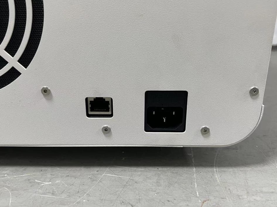
External Photos
Shenzhen CTB Testing Technology Co., Ltd. Report No.: CTB221009002RFX Report Tel: 4008-707-283 Web: http://www.ctb-lab.net Page 1 of 4 Model: P200, P200 HD, P200 UHD External Photos Shenzhen CTB Testing Technology Co., Ltd. Report No.: CTB221009002RFX Report Tel: 4008-707-283 Web: http://www.ctb-lab.net Page 2 of 4 Shenzhen CTB Testing Technology Co., Ltd. Report No.: CTB221009002RFX Report Tel: 4008-707-283 Web: http://www.ctb-lab.net Page 3 of 4 Shenzhen CTB Testing Technology Co., Ltd. Report No.: CTB221009002RFX Report Tel: 4008-707-283 Web: http://www.ctb-lab.net Page 4 of 4
ID Label/Location Info
Label Location
Internal Photos
Shenzhen CTB Testing Technology Co., Ltd. Report No.: CTB221009002RFX Report Tel: 4008-707-283 Web: http://www.ctb-lab.net Page 1 of 10 Model: P200, P200 HD, P200 UHD Internal Photos ANT Shenzhen CTB Testing Technology Co., Ltd. Report No.: CTB221009002RFX Report Tel: 4008-707-283 Web: http://www.ctb-lab.net Page 2 of 10 Shenzhen CTB Testing Technology Co., Ltd. Report No.: CTB221009002RFX Report Tel: 4008-707-283 Web: http://www.ctb-lab.net Page 3 of 10 Shenzhen CTB Testing Technology Co., Ltd. Report No.: CTB221009002RFX Report Tel: 4008-707-283 Web: http://www.ctb-lab.net Page 4 of 10 Shenzhen CTB Testing Technology Co., Ltd. Report No.: CTB221009002RFX Report Tel: 4008-707-283 Web: http://www.ctb-lab.net Page 5 of 10 Shenzhen CTB Testing Technology Co., Ltd. Report No.: CTB221009002RFX Report Tel: 4008-707-283 Web: http://www.ctb-lab.net Page 6 of 10 Shenzhen CTB Testing Technology Co., Ltd. Report No.: CTB221009002RFX Report Tel: 4008-707-283 Web: http://www.ctb-lab.net Page 7 of 10 Shenzhen CTB Testing Technology Co., Ltd. Report No.: CTB221009002RFX Report Tel: 4008-707-283 Web: http://www.ctb-lab.net Page 8 of 10 Shenzhen CTB Testing Technology Co., Ltd. Report No.: CTB221009002RFX Report Tel: 4008-707-283 Web: http://www.ctb-lab.net Page 9 of 10 Shenzhen CTB Testing Technology Co., Ltd. Report No.: CTB221009002RFX Report Tel: 4008-707-283 Web: http://www.ctb-lab.net Page 10 of 10
RF Exposure Info
FCC §15.247 (i), §2.1091 – RF Exposure FCC ID: 2A6ZN-P200 Applied procedures / limit According to FCC §15.247(i) and §1.1307(b)(1), systems operating under the provisions of this section shall be operated in a manner that ensures that the public is not exposed to radio frequency energy level in excess of the Commission’s guidelines. Limits for Occupational / Controlled Exposure Frequency Range (MHz) Electric Field Strength (E) (V/m) Magnetic Field Strength (H) (A/m) Power Density (S) (mW/ cm 2 ) Averaging Time |E| 2 ,|H| 2 or S (minutes) 0.3-3.0 614 1.63 (100)* 6 3.0-30 1842 / f 4.89 / f (900 / f)* 6 30-300 61.4 0.163 1.0 6 300-1500 F/300 6 1500-100,000 5 6 Note: ƒ is frequency in MHz * = Power density limit is applicable at frequencies greater than 100 MHz Limits for General Population / Uncontrolled Exposure Frequency Range (MHz) Electric Field Strength (E) (V/m) Magnetic Field Strength (H) (A/m) Power Density (S) (mW/ cm 2 ) Averaging Time |E| 2 ,|H| 2 or S (minutes) 0.3-1.34 614 1.63 (100)* 30 1.34-30 824/f 2.19/f (180/f)* 30 30-300 27.5 0.073 0.2 30 300-1500 F/1500 30 1500-100,000 1.0 30 Note: f = frequency in MHz * = Plane-wave equivalent power density MPE PREDICTION Predication of MPE limit at a given distance, Equation from OET Bulletin 65, Edition 97-01 Where: S = power density P = power input to antenna G = power gain of the antenna in the direction of interest relative to an isotropic radiator R = distance to the center of radiation of the antenna,R=20cm Test Result of RF Exposure Evaluation Tune up Produce power Maximu m peak output power (dBm) Output power to antenna (mW) Antenna Gain (numeric) Power Density (S) (mW/ cm2) Limit (mW / cm2 ) Result 2.4G WIFI 802.11b &2412 13±1 14 25.1189 2.1038 (3.23dBi) 0.01052 1 Pass
Test Report
Testing Report Gain and Efficiency Freq./MHz Peak Gain/dBi Efficiency/% 2400 3.10 61.0 2410 3.20 61.5 2420 3.23 62.2 2430 2.90 60.3 2440 2.88 60.0 2450 2.77 59.5 2460 2.72 59.1 2470 2.67 58.5 2480 2.64 58.2 2490 2.61 57.9 2500 2.57 57.6 Typical free space radiation pattern 2.4G pattern: (1) X-Z Plane: V Phi=0 (2) Y-Z Plane: V Phi=90 (3)X-Y Plane: H Theta=90 Ant enna Type value Antenna Types 2.4G Frequency range 2400-2500MHZ Antenna Gain 3.23dBI Impedance 50Ω Standing wave ratio S.W.R≤1.5 Polarization mode Linear polarization connector SMA Antenna size 95*13mm Manufacturer Information 深圳聚力成电子 Antenna picture
Test Report
Shenzhen CTB Testing Technology Co., Ltd. Report No.: CTB221009002RFX Report Tel: 4008-707-283Web: http://www.ctb-lab.net Page 1 of 64 TEST REPORT Compiled by: Reviewed by: Approved by: Chen Zheng Arron Liu Bin Mei / Director Note: If there is any objection to the inspection results in this report, please submit a written report to the company within 15 days from the date of receiving the report. The test report is effective only with both signature and specialized stamp. This result(s) shown in this report refer only to the sample(s) tested. Without written approval of Shenzhen CTB Testing Technology Co., Ltd. this report can’t be reproduced except in full. The tested sample(s) and the sample information are provided by the client. “*” indicates the testing items were fulfilled by subcontracted lab. “#” indicates the items are not in CNAS accreditation scope. Product Name: Industrial Photocurable 3D Printer FCC ID: 2A6ZN-P200 Trademark: Model Number: P200, P200 HD, P200 UHD Prepared For: Suzhou Laisai Intelligence Technology Co., Ltd Address: No.59 Jiangnan Avenue, Changshu City, Jiangsu Province, China Manufacturer: Suzhou Laisai Intelligence Technology Co., Ltd Address: No.59 Jiangnan Avenue, Changshu City, Jiangsu Province, China Prepared By: Shenzhen CTB Testing Technology Co., Ltd. Address: Floor 1&2, Building A, No. 26 of Xinhe Road, Xinqiao Community, Xinqiao Street, Baoan District, Shenzhen, Guangdong, China. Sample Received Date: Sep. 27, 2022 Sample tested Date: Sep. 27, 2022 to Oct. 09, 2022 Issue Date: Oct. 09, 2022 Report No.: CTB221009002RFX Test Standards FCC Part15.247 ANSI C63.10:2013 Test Results PASS Remark: This is WIFI-2.4GHz band radio test report. Shenzhen CTB Testing Technology Co., Ltd. Report No.: CTB221009002RFX Report Tel: 4008-707-283 Web: http://www.ctb-lab.net Page 2 of 64 TABLE OF CONTENT Test Report Declaration Page 1. VERSION .......................................................................... 3 2. TEST SUMMARY ................................................................... 4 3. MEASUREMENT UNCERTAINTY ..................................................... 5 4. PRODUCT INFORMATION AND TEST SETUP .......................................... 6 4.1 Product Information .................................................................... 6 4.2 Test Setup Configuration ............................................................... 6 4.3 Support Equipment .................................................................... 6 4.4 Channel List .......................................................................... 7 4.5 Test Mode ............................................................................ 7 4.6 Test Environment ...................................................................... 7 5. TEST FACILITY AND TEST INSTRUMENT USED ....................................... 8 5.1 Test Facility ........................................................................... 8 5.2 Test Instrument Used .................................................................. 8 6. AC POWER LINE CONDUCTED EMISSION ............................................ 10 6.1 Block Diagram Of Test Setup .......................................................... 10 6.2 Limit ................................................................................ 10 6.3 Test procedure ....................................................................... 11 6.4 Test Result .......................................................................... 12 7. RADIATED SPURIOUS EMISSION ................................................... 14 7.1 Block Diagram Of Test Setup .......................................................... 14 7.2 Limit ................................................................................ 14 7.3 Test procedure ....................................................................... 16 7.4 Test Result .......................................................................... 17 8. BAND EDGE AND RF COUNDUCTED SPURIOUS EMISSIONS .......................... 39 8.1 Block Diagram Of Test Setup .......................................................... 39 8.2 Limit ................................................................................ 39 8.3 Test procedure ....................................................................... 39 8.4 Test Result .......................................................................... 40 9. COUDUCTED OUTPUT POWER ..................................................... 48 9.1 Block Diagram Of Test Setup .......................................................... 48 9.2 Limit ................................................................................ 48 9.3 Test procedure ....................................................................... 48 9.4 Test Result .......................................................................... 49 10. 6DB OCCUPIED BANDWIDTH ....................................................... 50 10.1 Block Diagram Of Test Setup ......................................................... 50 10.2 Limit ............................................................................... 50 10.3 Test procedure ...................................................................... 50 10.4 Test Result ......................................................................... 51 11. POWER SPECTRAL DENSITY ...................................................... 56 11.1 Block Diagram Of Test Setup ......................................................... 56 11.2 Limit ............................................................................... 56 11.3 Test procedure ...................................................................... 56 11.4 Test Result ......................................................................... 57 12. ANTENNA REQUIREMENT ......................................................... 62 13. EUT TEST SETUP PHOTOGRAPHS .................................................. 63 (Note: N/A …
Text truncated - open the document above for the full version.
Test Setup Photos
Shenzhen CTB Testing Technology Co., Ltd. Report No.: CTB221009002RFX Report Tel: 4008-707-283 Web: http://www.ctb-lab.net Page 1 of 2 Model: P200, P200 HD, P200 UHD Radiated Emission Below 1G Above 1G Shenzhen CTB Testing Technology Co., Ltd. Report No.: CTB221009002RFX Report Tel: 4008-707-283 Web: http://www.ctb-lab.net Page 2 of 2 Conducted emissions
Contact Information
Applicant
Jianxin Lu(Certification Engineer)
Technical Contact
Test Firm
Shenzhen CTB Testing Technology Co., Ltd.Rita Xiao
[email protected]86-13538218145
Technical Specifications
| # | Rule Parts | Frequency Range | Power Output |
|---|---|---|---|
| 1 | 15C | 2.41 GHz - 2.46 GHz | 18.62 mW |
Other Applications from Suzhou Laisai Intelligence Technology Co.,Ltd
2A6ZN-EDGEE2
Apr 09, 2024Desktop Photocurable 3D Printer
Equipment Class
NII - Unlicensed National Information Infrastructure TX2A6ZN-EDGEMAX
Jan 29, 2024Industrial Photocurable 3D Printer
Equipment Class
NII - Unlicensed National Information Infrastructure TX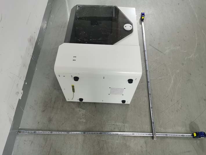
2A6ZN-EDGE-E1
Nov 09, 2022Desktop Photocurable 3D Printer
Equipment Class
DTS - Digital Transmission System