2A7RF-LT102XKUWB Mini radar module
Xandar Kardian Inc.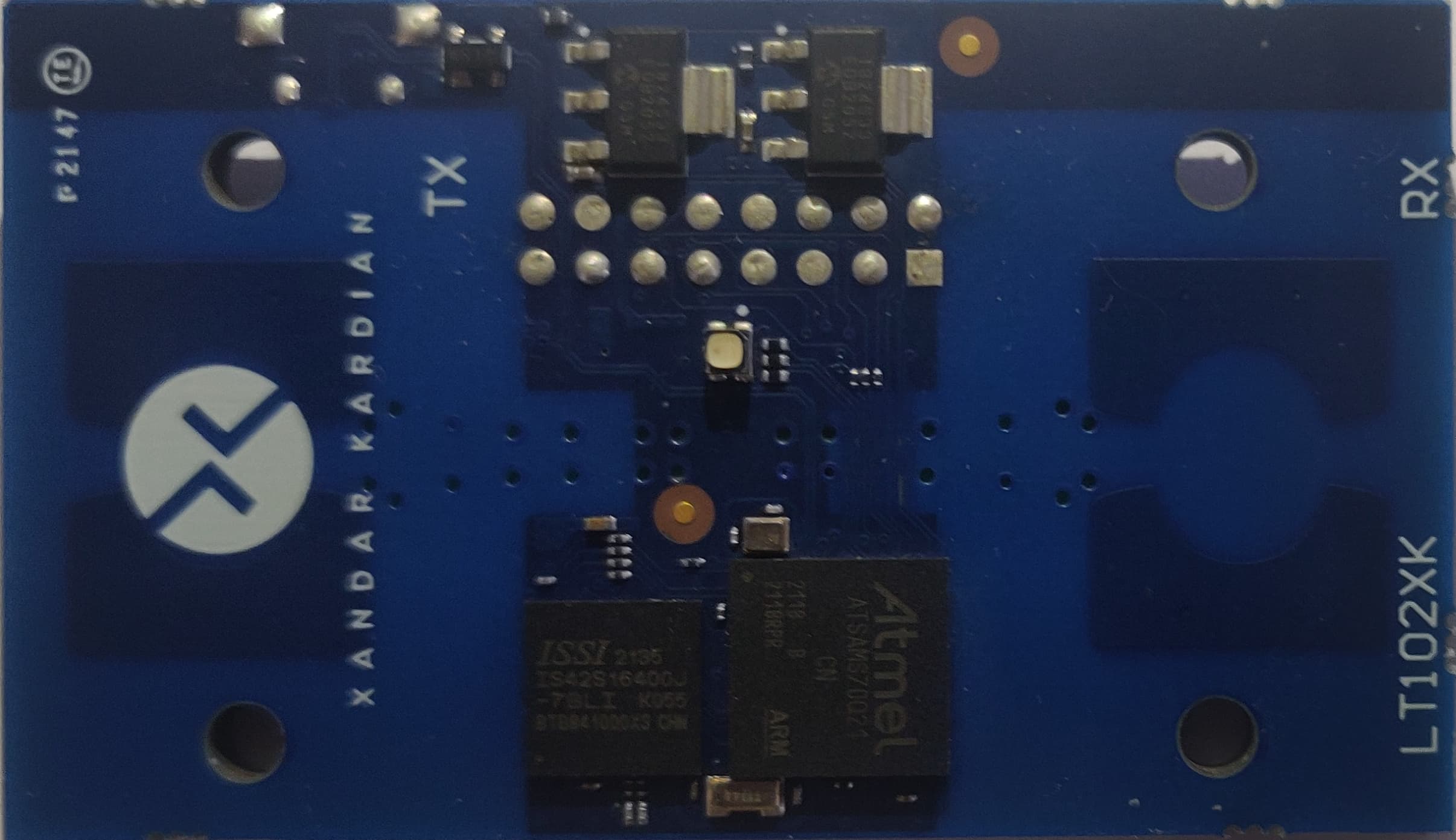
Click to zoom
Application Details
- Equipment Class
- UWB - Ultra Wideband Transmitter
- Date of Grant
- Jan 29, 2023
- Application Purpose
- Original Equipment
- Date of Application
- Dec 12, 2022
- Equipment Note
- UWB Mini radar module
- Frequency Range
- 6642.30000000 - 7882.40000000
- Company
- Xandar Kardian Inc.
- Country
- United States
Documents & Files
Document Text
Text extracted from the exhibit documents filed with the FCC. Open a document above to read the original.
Users Manual
LT102XK UWB Radar Module Datasheet | Rev.1.1 LT102XK UWB Radar Module Pag. 1 of 9 Datasheet | Rev.1.1 LT102XK UWB Radar Module Datasheet | Rev.1.1 1 Summary LT102XK radar module is a turn-key Ultra-Wide Band radar system for indoor applications. LT102XK integrates high- end directive UWB antennas, the signal processing unit, and the communication interfaces. It is designed to fit EU EN 302 065 (EU), FCC CFR 47 Part 15 (USA), RS220 03/2009 (Canada), UWB Regulations. General Specifications • Typ. Detection range: up to 12 meters • Maximum power consumption: 200mA@5V • Operating frequency: 6.5GHz to 8.5GHz • Power supply: 5Vdc or USB 5Vdc • Temperature range: -40°C to +85°C • Integrated Antenna (aperture ±60° by ±60°) • Communication interfaces: USB full speed, SPI, UART • Dimensions: 36mm x 68mm Applications: • Presence detection • Position tracking • Breath detection and monitoring • People counting • Gesture recognition Table of contents 1 Summary ........................................................................................................... 1 2 Features ............................................................................................................ 2 3 Operating Principle ............................................................................................ 2 4 Electrical specification ........................................................................................ 3 5 Block Diagram ................................................................................................... 3 LT102XK UWB Radar Module Datasheet | Rev.1.1 Pag. 2 of 9 6 Module connection ............................................................................................ 4 6.1 USB operation ................................................................................................ 4 6.2 Auxiliary IO connector..................................................................................... 4 7 Antenna Performances ...................................................................................... 5 2 Features The LT102XK is a high configurable UWB radar. This module combines a full UWB transceiver and an on board MCU. The module is targeted for application like presence detection, position tracking, breath detection and analysis. The communication is achieved by an USB full speed (virtual com port). The module has an auxiliary connector that may be used as GPIOs or additional communication interface such as SPI and UART. The module is USB powered. 3 Operating Principle The operating principle of the system is based on the direct readout of the backscattered pulse • The transmitter emits pulses (Fig. 1a) which travels into space and hits the targets that are into active area of the radar • The targets reflect part of the incoming energy (echoes) backward to the radar module (Fig. 1b). • The receiver converts the incoming signal to digital data, these data are provided to the MCU and processed according to the application. LT102XK UWB Radar Module Pag. 3 of 9 Datasheet | Rev.1.1 Fig. 1: The basic principle and the waveforms 4 Electrical specification Min Typ Max Operating frequency 6.5GHz 7.29GHz 8.5GHz Mean e.i.r.p. density -41.3dBm/MHz Peak e.i.r.p. density 0dBm/50MHz Supply voltage (USB) 4.5Vdc 5Vdc 5.5Vdc Current consuption (AuxIO) 120mA 200mA Range resolution 6mm V IL 0.3 Vdd V IH 0.7Vdd R series (AuxIO protection) 220 Ohm 5 Block Diagram The block diagram of the LT102XK is reported next. LT102XK UWB Radar Module Datasheet | Rev.1.1 Pag. 4 of 9 Fig. 2 LT102XK System Diagram 6 Module connection 6.1 USB operation In a default configuration, the LT102XK module can be attached to a PC through a A-plug, micro-B USB cable. In this configuration, the power supply of the LT102XK is taken from the +Vcc pin of the USB cable. Fig. 3: Plug and Play configuration. 6.2 Auxiliary IO connector The module provides an auxiliary connector (AuxIO) that may be used to control external electronics, or as alternate communication interface (SPI and/or UART). When both the USB plug and the AuxIO connector are connected the power supply is taken from USB connector. Pin Description LT102XK UWB Radar Module Pag. 5 of 9 Datasheet | Rev.1.1 1 Vext: External Power Supply 2 Gnd: External Ground 3 RXD: UART Interface RX 4 TXD: UART Interface Tx 5 SPI0_CLK: SPI Interface #0, CLK Signal 6 SPI0_CS2: SPI Interface #0, Chip Select (active low) 7 RST: Reset (active low) 8 TDO: JTAG Interface TDO 9 SWCLK/TCLK: JTAG Interface CLK / Serial Wire Debug Interface CLK 10 TMS/SWDIO: JTAG Interface TSM / Serial Wire Debug Interface TMS 11 IO0: General Purpose I/O 0 12 IO1: General Purpose I/O 1 13 TDI: JTAG Interface TDI 14 ERASE: Erase internal flash. Leave open. To erase device flash connect to Vdd during startup 15 SPI0_MOSI: SPI Interface #0, MOSI 16 SPI0_MISO: SPI Interface #0, MISO Table 1: AuxIO Pinout description 7 Antenna Performances Antenna data are reported @ 7.5GHz. Maximum gain is 5.6dBi with HPBW = 71° x 84° LT102XK UWB Radar Module Datasheet | Rev.1.1 Pag. 6 of 9 Fig. 4 Antenna Diagram and X-Z plane cut Fig. 5 Aligned View of X-Z plane Fig. 6 Antenna Gain over X-Z plane LT102XK UWB Radar Module Pag. 7 of 9 Datasheet | Rev.1.1 Fig. 7 Antenna Diagram and Y-Z plane cut Fig. 8 Aligned View of Y-Z plane 8 Restriction • In accordance with Commission Decision 2000/299/CE of 6 April 2000, the device is classified as Class I, Subclass 57e “Equipment using Ultra-Wideband Technology (Location tracking systems)” • The LT102XK is a Class I, Subclass 57e device. It is intended for indoor and in-vehicle use only. • The LT102XK is sensitive to direct sun and visible/IR light. It is recommended to shield it. LT102XK UWB Radar Module Datasheet | Rev.1.1 Pag. 8 of 9 • To guarantee the maximum detection distance (10m) the LT102XK must be kept at least 2m away from a 5GHz WiFi device. • If the maximum range is less or equal than 5m, there is no minimum distance to 5GHz WiFi devices 9 Regulatory Information US…
Text truncated - open the document above for the full version.
Cover Letter(s)
Cover Sistemi- 2022 Confidential LT102XK Shielding Strategy Introduction This document illustrates the shielding strategy adopted for the LT102XK device. According to https://transition.fcc.gov/oet/ea/presentations/files/oct16/23-Equipment-Authorization- Modular-Devices-101216-JS.pdf , the shield is required to “prevent (near field) coupling between the RF circuitry and any y wires or circuits (traces) on the host. “ In the LT102XK, the shield is realized by the conductive silicon layer which is on top of the RF circuit. In detail the WLCSP technology is exploited to “embed” the active devices of the RF section in between board ground and the above-mentioned conductive layer. As demonstrated by means of full 3D EM Simulations, we demonstrate that the shielding of LT102XK makes the requirement of an extra shielding redundant and useless. WLCSP Technology WLCSP technology is a “package-less” where “under-bumps” (UBM, Under Bump Metallization) are used to solder the chip to the PCB Figure 1 Cross Section of a WLCSP Integrated Circuit 1. Therefore, w.r.t. normal packaging techniques, the chip is actually flipped. This means that silicon substrate is “far” from the host board while silicon metal layers are close to the PCB and its ground plane. 2. This is the opposite w.r.t. normal packaging where silicon substrate is close to the PCB while on-chip metal layers are When mounted on top of a Printed Circuit Board, the resulting stack-up is as follows. Figure 2 WLCSP Integrated Circuit Mounted on top of a PCB Normal Packaging While a normal package is depicted below Figure 3 Normal IC Packaging In “normal” packaging the silicon layer is in-between the active devices (transistors, inductors etc.) which are part of the Integrated Circuit. As a result, they “lie” on top of the circuit: In normal packaging, no shielding is therefore available in this case. Substrate as conductive layer In LT102XK, all integrated devices which are part of the RF circuit are in between PCB ground and the substrate which contains few undoped areas (all integrated devices require a solid connection either to ground or power supply and this is realized by highly conductive doped areas). In LT102XK we exploit the WLCSP “flip-chip”, along with substrate doping to act as a shield. While undoped silicon is a poor conductor (making it a poor shield), CMOS processes uses two different doping options (NDIFF, PDIFF) which make the silicon substrate a very good conductor. For reference, the silicon process used for the LT102XK front-end shows the following parameters (approx.): Undoped silicon 1e-3 S/m PDIFF 7e6 S/m NDIFF 11e3 S/m Sides With respect of the “sides” of the devices, the RF integrated circuit is 0.7mm thick. Operating at maximum 8.5GHz frequency (wavelength=35.3mm), this corresponds to an aperture = 0.0198 λ. Demonstration of the shielding properties The effectiveness of the shielding strategy is demonstrated by means of EM Simulations. Given the requirement of preventing near-field interactions, the electric/magnetic field is evaluated with “near-field” sensors placed all over the integrated circuit. No far-field sensor is considered as all spurious radiation properties have been already verified in the anechoic chamber (see attached test reports). To allow for a feasible EM model (i.e. a simulation with all the geometries inside the IC would be undoable given the size of the resulting mesh) we have modeled a resonating LC tank whose resonating frequency is @7.8GHz, inside the operating bandwidth of the device. The LC resonating tank is selected to maximize currents and magnetic fields, in order to highlight the effectiveness of the shielding. Simulations are done by means of Keysight EmPRO 2022 (Cyndaquil). Simulation type: FEM. Conductor modeled as surface impedances. Solver SDS with mixed 1 st / 2 nd order basis. Adaptive meshing with max error on S-Params = 0.03 is enforced. Near-fields are extracted at chip surfaces. To demonstrate the effectiveness of the shielding strategy, in the following tests are performed: 1. “Floating Chip”: no shield is provided either at top / bottom level; 2. “Normal Packaging”: LC tank is on top of the PCB-Substrate-BEOL (BackEnd Of Line); 3. “LT102XK”: LC tank is in-between substrate and PCB ground; 4. Shield: the LC tank is shielded by a commercial shield The 3D EM models are reported in the next pictures. Description of the EM (electromagnetics models) and simulations The 3D model of the LC tank is reported in the next picture. Figure 4 Detail on the active RF circuit Physical details of the substrate and of metal interconnections are extracted by the foundry PDK (Process Development Kit). Figure 5 EM Model for the “floating chip” Figure 6 EM Model for the active Circuit in the "normal packaging scheme" Figure 7 EM Model for the active Circuit in the LT102XK Figure 8 EM Model for the normal package + shield Results: Fields on Surfaces Case 1.: Floating Chip Surface currents are shown in the next pictures. Top Face Figure 9 Surface E-Field Magnitude at top of the chip (BEOL side) for the unshielded case Figure 10 Surface H-Field Magnitude at top passivation layer for the unshielded case Sides Figure 11 Surface E-Field Magnitude at chip sides for the unshielded case Figure 12 Surface H-Field Magnitude at chip sides for the unshielded case Case 2: Normal Packaging Top Face Figure 13 Surface E-Field Magnitude at top of the chip for normal packaging Figure 14 Surface H-Field Magnitude at top of the chip for normal packaging Sides Figure 15 Surface E-Field Magnitude at chip sides for normal packaging Figure 16 Side H-Field Magnitude at chip side for normal packaging Case 3: LT102XK The LT102XK active RF circuit is modeled as in Figure 7: the flipped chip is mounted over the PCB. Underneath the RF circuit the Groud plane is modeled as a 1/2oz (17um thick) copper shield. Top Face Figure 17 Surface E-Field Magnitude at top of the chip for the LT102XK Figure 18 Surface H-Field Magnitude at…
Text truncated - open the document above for the full version.
Cover Letter(s)
Xandar Kardian Inc. 17 State Street #4000 New York, NY 10004 USA Nemko North America, Inc. 303 River Road Ottawa, Ontario, Canada K1V 1H2 AUTHORITY TO ACT AS AGENT - FCC On our behalf, I appoint Nemko North America, Inc., to act as our agent in the preparation of this application for equipment certification. I certify that submitted documents properly describe the device or system for which equipment certification is sought. I also certify that each unit manufactured, imported or marketed, as defined in FCC regulations will have affixed to it a label identical to that submitted for approval with this application. In signing this letter, Applicant certifies that neither the applicant nor any party to the application is not subject to a denial of Federal benefits, that include FCC benefits, pursuant to Section 5301 of the Anti- Drug Abuse Act of 1988, 21 U.S.C. § 862 because of a conviction for possession or distribution of a controlled substance. See 47 CFR 1.2002(b) for the definition of a "party" for these purposes. For instances where our authorized agent signs the application for certification on our behalf, I acknowledge that all responsibility for complying with the terms and conditions for certification, as specified by Nemko North America Inc., still resides still resides with us. Sincerely, Signed: Dated: 2022-07-07 Printed name: Sam Yang Title: CEO Company Name: Xandar Kardian Inc.
Cover Letter(s)
Xandar Kardian Inc. 17 State Street #4000 New York, NY 10004 USA Modular Approval Request FCC ID: 2A7RF-LT102XK The following attestation addresses the requirements to support modular approval: Modular approval requirement Yes (provide brief statement) No * (a) The radio elements must have the radio frequency circuitry shielded. Physical components and tuning capacitor(s) may be located external to the shield, but must be on the module assembly YES Frequency Shielding is provided by internal Ground layers. RF Lines to/from antennas from/to txr are annealed inside the PCB and differential non-radiating Ground Coplanar Waveguide mode is established from TxR to antennas No RF components other than TxR and antennas are present. Shielding on top side is provided by internal conductive layer on top of TxR. (b) The module must have buffered modulation/data inputs to ensure that the device will comply with Part 15 requirements with any type of input signal YES No data inputs are provided to the interface of the module. (c) The module must contain power supply regulation on the module YES LDOs are provided to generate internal power-supply lines See schematics (d) The module must contain a permanently attached antenna, or contain a unique antenna connector, and be marketed and operated only with specific antenna(s), per Sections 15.203, 15.204(b), 15.204(c), 15.212(a), 2.929(b) YES Module has PCB-embedded antenna (e) The module must demonstrate compliance in a stand-alone configuration YES Module has its own MCU and FW. It is designed to operate in stand-alone mode (f) The module must be labelled with its permanently affixed FCC ID label, or use an electronic display (See KDB Publication 784748 about labelling requirements) YES Labelling is attached to box. (g) The module must comply with all specific rules applicable to the transmitter. The grantee must provide comprehensive instructions to explain compliance requirements YES See test reports (h) The module must comply with RF exposure requirements YES See test reports * Please provide a detailed explanation if the answer is “No.” Sincerely, Signed: Dated: 2022-07-07 Printed name: Sam Yang Title: CEO Company Name: Xandar Kardian Inc.
Cover Letter(s)
Xandar Kardian Inc. 17 State Street #4000 New York, NY 10004 USA Nemko North America, Inc. 303 River Road Ottawa, Ontario, Canada K1V 1H2 REQUEST FOR CONFIDENTIALITY - FCC FCC ID: 2A7RF-LT102XK Pursuant to Sections 0.457(d) and 0.459 of the Commission’s Rules and FCC Guidance document 726920, we hereby request permanent confidential treatment of exhibits identified as such in the table below and request they are permanently withheld from public review based on the documents containing trade secrets and proprietary information not customarily released to the public. The public disclosure of this information might be harmful to the applicant and provide unjustified benefits to its competitors. We also request short-term confidentiality on certain exhibits until the intended date of marketing as outlined below. We request the exhibits be withheld from public view for a period of insert number of days (cannot exceed 180 days) days. We attest marketing of the product will only commence after the period of short-term confidentiality expires, or if marketing is to commence before the requested number of days listed above, the grantee will inform Nemko to release the Short-Term Confidentiality information withheld on the FCC equipment authorization website. Exhibit Type of Confidentiality Requested Block Diagrams ☒ Permanent ☐ Short Term External Photos ------------------ ☐ Short Term Internal Photos ☐ Permanent* ☐ Short Term Operation Description ☒ Permanent ☐ Short Term Parts List & Placement/BOM ☒ Permanent ☐ Short Term Tune-Up Procedure ☐ Permanent ☐ Short Term Schematic Diagrams ☒ Permanent ☐ Short Term Test Setup Photos ------------------ ☐ Short Term User’s Manual ☐ Permanent* ☐ Short Term The asterisked items (*) require further information to be provided in this justification letter before permanent confidentiality will be extended to these exhibits. Please refer to FCC KDB 726920 D01 found at: https://apps.fcc.gov/oetcf/kdb/forms/FTSSearchResultPage.cfm?switch=P&id=41731 and review section II, 3) regarding specific information that must accompany these requests. Note: any documents held under the Short-Term confidentiality will automatically become public after the requested time if an appropriate extension request has not been received. Any exhibits (i.e., schematic diagrams) that may have already been requested to have “Permanent” confidentiality as shown above need not be repeated under Short-Term confidentiality request. Sincerely, Signed: Dated: 2022-07-07 Printed name: Sam Yang Title: CEO Company Name: Xandar Kardian Inc.
Cover Letter(s)
LT102XK Antenna Report Rev. 1.0 Data: 12/01/2023 Author: Alessio Cacciatori POC: [email protected] Copyright © 2018 Cover Sistemi Srl LT102XK Antenna Report Pag. 1 of 5 Rev. 1.0 LT102XK Antenna Report Rev. 1.0 1 Revision History Rev Date Description 1.0 12 th , Jan., 2023 Issued 2 Introduction The LT102XK device is a single-PCB (Printed Circuit Board) micro-radar module. It is a pulsed radar operating into the 6.5GHz-8.5GHz frequency range. It includes an RF transceiver, directive antennas and a microprocessor for data processing and transceiver management. The LT102XK includes a transmitter, a receiver, an antenna connected to transmitter and an antenna connected to the receiver. Antennas are part of the PCB module and they cannot be changed by the user. Figure 1 Picture of LT102XK The typical applications of the LT102XK include: • Presence detection • Distance measuring • Breathe detection 2.1 Antenna Description The antennas are specifically designed to operate with the selected front-end (X4). The RF front-end has fully nominal 100Ω ports at both Tx and Rx side. Two differential CPWG (Grounded CoPlanar WaveGuide) lines brings the signal from the X4 RF I/Os to the antenna. LT102XK Antenna Report Rev. 1.0 Pag. 2 of 5 Figure 2 Picture with RF part, Antennas and Antennas Feeding lines highlighted (bottom side) Figure 3 Picture with Antennas highlighted (top side) Antennas are shown in the previous Figure 2 and Figure 3. On the back side a Ground Plane is clearly visible. Lines to/from RF transceiver are shown. They are differential Grounded Coplanar Waveguides (CPWG) lines and they are designed to provide good power matching in between RF Front-end and the antenna feeding points. Due to the differential nature of the selected front-end and due to the small pitch of positive/negative signals of the differential pairs (0.4mm pitch at RF Front-end, 0.75mm at antenna feeding points), it is extremely difficult to perform dedicate measurements on the antenna. The design/validation flow therefore relied on: 1. Selection of high-performance substrate with known and proven repeatability of its RF performances (dielectric constant, loss factor) LT102XK Antenna Report Pag. 3 of 5 Rev. 1.0 2. Validation of the design by means of an industry-approved simulator. This was Keysight® EmPRO® . The design was simulated by means of a full 3D FEM model. 3. Measurements of radiation properties of the entire devices 2.2 Simulation Details In order to obtain reliable results of the simulations, and considering that those antennas are specifically design for the LT102XK module, the performances of the antenna are calculated by modeling all geometries of the LT102XK module. Figure 4 EM Model 2.3 Antenna Simulated Performances The 3D radiation diagram of the Tx antenna is reported in the next pictures (same colormap apply also to the left pictures). 7GHz Front Side 7GHz Back side 7.5GHz Front Side 7.5GHz Back side LT102XK Antenna Report Rev. 1.0 Pag. 4 of 5 8GHz Front Side 8GHz Back Side 8.5GHz Front Side 8.5GHz Back Side 9GHz Front Side 9GHz Back Side LT102XK Antenna Report Pag. 5 of 5 Rev. 1.0 9.5GHz Front Side 9.5GHz Back Side Other relevant performances are shown in the next table. Performance @ 7.5GHz Value Total Efficiency 70% Maximum Realized Gain 5.65 dB 3dB Angular Width (azimuth/elevation) 71° / 84° Front to Back Ratio 15.0dB Main Lobe Direction (azimuth/elevation) 0° / 5° Axial Ratio (Az/El Probe Field @ 13dB WiFi 5.8GHz Attenuation (max RlzdGain @ 5.8GHz / max RlzdGain @ 7.5GHz ) 14dB S11<-10dB Bandwidth 7GHz to 9.7GHz
Cover Letter(s)
§ 15.521 Technical requirements applicable to all UWB devices (a) UWB devices may not be employed for the operation of toys. Operation onboard an aircraft, a ship or a satellite is prohibited. [R] this statement is reported in the User Manual. (b) Manufacturers and users are reminded of the provisions of §§ 15.203 and 15.204. [R] § 15.203: the antenna is integral, not detachable (for details, see document “LT102XK_AntennaReport”). § 15.204: neither radio frequency power amplifiers, or any kind of antenna modification are allowed by design (c) Emissions from digital circuitry used to enable the operation of the UWB transmitter shall comply with the limits in § 15.209, rather than the limits specified in this subpart, provided it can be clearly demonstrated that those emissions from the UWB device are due solely to emissions from digital circuitry contained within the transmitter and that the emissions are not intended to be radiated from the transmitter's antenna. Emissions from associated digital devices, as defined in § 15.3(k), e.g., emissions from digital circuitry used to control additional functions or capabilities other than the UWB transmission, are subject to the limits contained in Subpart B of this part. [R] for the emissions from digital circuitry used to enable the operation of the UWB transmitter, see the test report n. 462409-2TRFWL issued by Nemko S.p.A., § 7.6 “Radiated emissions”. For the emissions from digital circuitry, see the test report n. 462409-2TRFEMC issued by Nemko S.p.A.. (d) Within the tables in §§ 15.509, 15.511, 15.513, 15.515, 15.517, and 15.519, the tighter emission limit applies at the band edges. Radiated emission levels at and below 960 MHz are based on measurements employing a CISPR quasi-peak detector. Radiated emission levels above 960 MHz are based on RMS average measurements over a 1 MHz resolution bandwidth. The RMS average measurement is based on the use of a spectrum analyzer with a resolution bandwidth of 1 MHz, an RMS detector, and a 1 millisecond or less averaging time. Unless otherwise stated, if pulse gating is employed where the transmitter is quiescent for intervals that are long compared to the nominal pulse repetition interval, measurements shall be made with the pulse train gated on. Alternative measurement procedures may be considered by the Commission. [R] § 15.519(c) is applicable: CISPR quasi-peak detector at and below 960 MHz has been used for radiated emissions, as well as an RMS detector with 1 MHz RBW for measurements above 960 MHz, with tighter emission limits adopted at the band edges (for details, see the test report n. 462409-2TRFWL issued by Nemko S.p.A., § 7.6 “Radiated emissions”). (e) The frequency at which the highest radiated emission occurs, fM, must be contained within the UWB bandwidth. [R] the frequency at which the highest radiated emission occurs is contained within the UWB bandwidth (the allowed frequency band is 3100-10600 MHz according to § 15.519(b)) – see Table 7.5-2 of the test report n. 462409-2TRFWL issued by Nemko S.p.A.. (f) Imaging systems may be employed only for the type of information exchange described in their specific definitions contained in § 15.503. The detection of tags or the transfer or data or voice information is not permitted under the standards for imaging systems. [R] not applicable. (g) When a peak measurement is required, it is acceptable to use a resolution bandwidth other than the 50 MHz specified in this subpart. This resolution bandwidth shall not be lower than 1 MHz or greater than 50 MHz, and the measurement shall be centered on the frequency at which the highest radiated emission occurs, fM. If a resolution bandwidth other than 50 MHz is employed, the peak EIRP limit shall be 20 log (RBW/50) dBm where RBW is the resolution bandwidth in megahertz that is employed. This may be converted to a peak field strength level at 3 meters using E(dBuV/m) = P(dBm EIRP) + 95.2. If RBW is greater than 3 MHz, the application for certification filed with the Commission must contain a detailed description of the test procedure, calibration of the test setup, and the instrumentation employed in the testing. [R] see § 7.5 of the test report n. 462409-2TRFWL issued by Nemko S.p.A.. (h) The highest frequency employed in § 15.33 to determine the frequency range over which radiated measurements are made shall be based on the center frequency, fC, unless a higher frequency is generated within the UWB device. For measuring emission levels, the spectrum shall be investigated from the lowest frequency generated in the UWB transmitter, without going below 9 kHz, up to the frequency range shown in § 15.33(a) or up to fC + 3/(pulse width in seconds), whichever is higher. There is no requirement to measure emissions beyond 40 GHz provided fC is less than 10 GHz; beyond 100 GHz if fC is at or above 10 GHz and below 30 GHz; or beyond 200 GHz if fC is at or above 30 GHz. [R] see § 7.1 of the test report n. 462409-2TRFWL issued by Nemko S.p.A.. (i) The prohibition in § 2.201(f) and 15.5(d) of this chapter against Class B (damped wave) emissions does not apply to UWB devices operating under this subpart. [R] considered. (j) Responsible parties are reminded of the other standards and requirements cross referenced in § 15.505, such as a limit on emissions conducted onto the AC power lines. [R] § 15.505(a) considered: . § 15.201(b) applicable and adopted . § 15.202 not applicable . § 15.203: the antenna is integral, not detachable (for details, see document “LT102XK_AntennaReport”) . § 15.204: neither radio frequency power amplifiers, or any kind of antenna modification are allowed by design . § 15.207 not applicable
ID Label/Location Info
Xandar Kardian Inc. Model: LT102XK FCC ID: 2A7RF -LT102XK IC: 28756-LT102XK
Test Report
TEST REPORT Electromagnetic Compatibility Report Reference No. .............. : 462409-2TRFEMC Date of issue .............................. : 2022-06-01 Test Report Verdict .................... : PASS Testing Laboratory ................... : Nemko S.p.A. Address ...................................... : Via Del Carroccio, 4 City ............................................ : 20853 Biassono (MB) Country ...................................... : Italy Testing location .......................... : Described at clause 1.4 Customer name ........................ : Xandar Kardian Inc Customer information ................. : 17 State Street #4000, 10004 New York (US) Reference standards ................ : FCC CFR 47 Part 15 Subpart B Standard application .................. : Full application Equipment under test .............. : Ultra Wide Band (UWB) Radar sensor module Trademark(s) ............................. : Manufacturer .............................. : Xandar Kardian Inc. Model/Type reference ................ : Described at clause 4.1 Tests performed by .................... : D. Guarnone Report approved by .................... : R. Giampaglia Report n° 462409-2TRFEMC page 2 / 27 CONTENTS 1. GENERAL INFORMATION .............................................................................................. 3 1.1 Project history ......................................................................................................................................... 3 1.2 Symbol used in the report ....................................................................................................................... 3 1.3 Date of sample(s) reception and tests .................................................................................................... 3 1.4 Testing location ....................................................................................................................................... 4 1.5 Environmental conditions ....................................................................................................................... 4 1.6 Measurement uncertainty and assessment of conformity ..................................................................... 4 1.7 Instruments calibration table .................................................................................................................. 6 2. PRODUCT STANDARDS, TEST METHODS AND TECHNICAL PROCEDURES ........…
Text truncated - open the document above for the full version.
Contact Information
Applicant
Sam Yang(CEO)
Test Firm
Nemko S.p.A.Roberto Giampaglia
Technical Specifications
| # | Rule Parts | Frequency Range | Power Output |
|---|---|---|---|
| 1 | 15F | 6.64 GHz - 7.88 GHz | - |