2A7WS-MGT1301Moeco ACT Sensor
Moeco IoT Inc.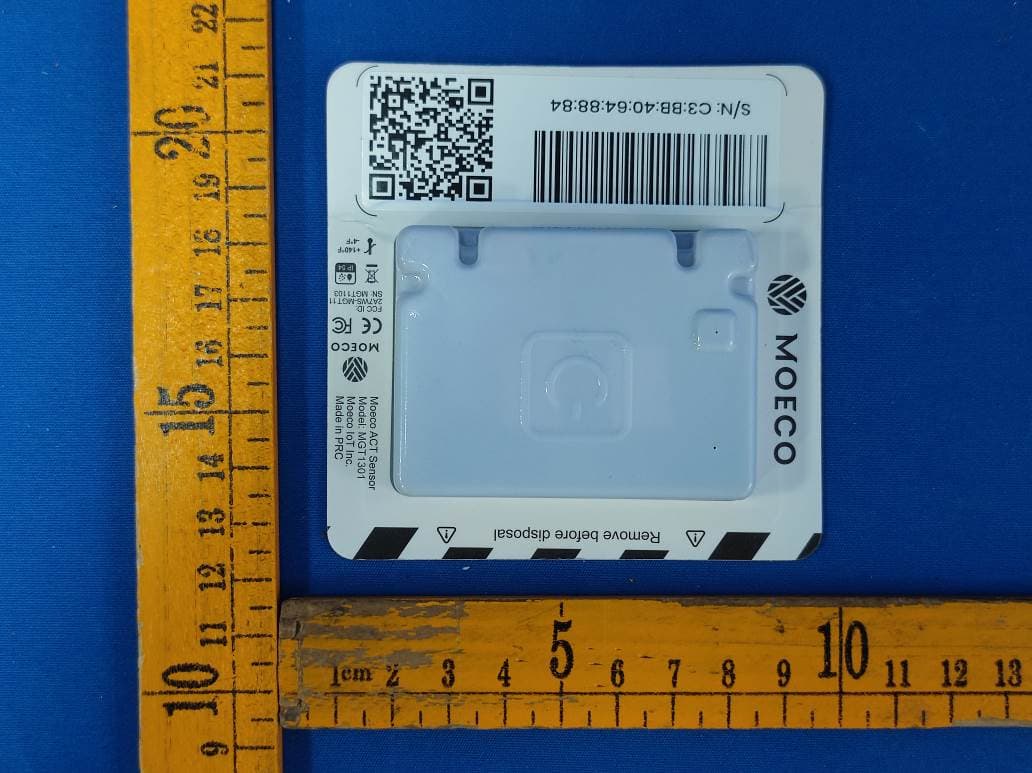
Click to zoom
Application Details
- Equipment Class
- DTS - Digital Transmission System
- Date of Grant
- Jun 26, 2023
- Application Purpose
- Original Equipment
- Date of Application
- Jun 26, 2023
- Equipment Note
- Moeco ACT Sensor
- Frequency Range
- 2402.00000000 - 2480.00000000
- Company
- Moeco IoT Inc.
- Country
- United States
Documents & Files
Document Text
Text extracted from the exhibit documents filed with the FCC. Open a document above to read the original.
Users Manual
GLOBAL SENSOR MGT1301 User manual M-1301/001 2023-06-15 Moeco IoT Inc. | 440 N Wolfe Road, Sunnyvale, CA, 94085 USA | moeco.io TABLE OF CONTENTS 1. LEGAL INFORMATION. . . . . . . . . . . . . . . . . . . . . . . . . . . . . . . .1 1.1 Liability disclaimer. . . . . . . . . . . . . . . . . . . . . . . . . . . . . . . . . .1 1.2 Copyrights. . . . . . . . . . . . . . . . . . . . . . . . . . . . . . . . . . . . . . . .1 1.3 Trademarks. . . . . . . . . . . . . . . . . . . . . . . . . . . . . . . . . . . . . . .1 1.4 Compliance. . . . . . . . . . . . . . . . . . . . . . . . . . . . . . . . . . . . . . .1 1.4.1 EU Declaration of Conformity. . . . . . . . . . . . . . . . . . . . .1 1.4.2 Federal Communications Commission (FCC) Notice. . . . .2 1.5 Radio Frequency Notice. . . . . . . . . . . . . . . . . . . . . . . . . . . . . . .3 1.6 Company legal address. . . . . . . . . . . . . . . . . . . . . . . . . . . . . .3 2. PREFACE. . . . . . . . . . . . . . . . . . . . . . . . . . . . . . . . . . . . . . . . . .3 2.1 User description. . . . . . . . . . . . . . . . . . . . . . . . . . . . . . . . . . . .3 2.2 Conventions. . . . . . . . . . . . . . . . . . . . . . . . . . . . . . . . . . . . . .3 2.3 Retaining information. . . . . . . . . . . . . . . . . . . . . . . . . . . . . . . .4 2.4 Obtaining documentation. . . . . . . . . . . . . . . . . . . . . . . . . . . . .4 2.5 Feedback. . . . . . . . . . . . . . . . . . . . . . . . . . . . . . . . . . . . . . . .4 3. DESCRIPTION OF THE DEVICE. . . . . . . . . . . . . . . . . . . . . . . . .4 3.1 Monitoring shipments. . . . . . . . . . . . . . . . . . . . . . . . . . . . . . . .5 3.2 Flight mode. . . . . . . . . . . . . . . . . . . . . . . . . . . . . . . . . . . . . . .6 3.3 Technical specifications. . . . . . . . . . . . . . . . . . . . . . . . . . . . . .6 4. PREPARATION FOR USE. . . . . . . . . . . . . . . . . . . . . . . . . . . . . .8 4.1 Package contents. . . . . . . . . . . . . . . . . . . . . . . . . . . . . . . . . . .8 4.2 Identifying the device. . . . . . . . . . . . . . . . . . . . . . . . . . . . . . . .8 5. SAFETY MEASURES. . . . . . . . . . . . . . . . . . . . . . . . . . . . . . . . . .9 6. OPERATING THE DEVICE. . . . . . . . . . . . . . . . . . . . . . . . . . . . . .10 6.1 At departure. . . . . . . . . . . . . . . . . . . . . . . . . . . . . . . . . . . . . .10 6.2 On arrival. . . . . . . . . . . . . . . . . . . . . . . . . . . . . . . . . . . . . . . .11 7. TROUBLESHOOTING. . . . . . . . . . . . . . . . . . . . . . . . . . . . . . . . .12 8. STORAGE. . . . . . . . . . . . . . . . . . . . . . . . . . . . . . . . . . . . . . . . . .12 9. DISPOSAL AND RECYCLING. . . . . . . . . . . . . . . . . . . . . . . . . . .13 9.1 Disposal of electronic components. . . . . . . . . . . . . . . . . . . . . . .13 9.2 Disposal of batteries. . . . . . . . . . . . . . . . . . . . . . . . . . . . . . . . .13 9.3 Disposal of packaging waste. . . . . . . . . . . . . . . . . . . . . . . . . . .13 i 1. LEGAL INFORMATION 1.1 Liability disclaimer Moeco IoT, Inc. (hereinafter “Moeco”) will not be held liable for damage resulting from failure to comply with the instructions and warnings provided in this document. Moeco reserves the right to revise this document at any time under no obligation to notify any person of the revision. User shall observe all pertinent state, regional, and local safety regulations when installing and using this device. The information provided in this document contains general description and technical characteristics of the device as well as instructions addressed to the user of the device. Failure to observe these instructions can lead to the damage of the device described in this document. 1.2 Copyrights All reproduction rights of this document are reserved to Moeco. Any reproduction of the text and illustrations, even partial, is prohibited. The information herein cannot be disclosed to third parties without the written consent of Moeco which has exclusive property thereof. 1.3 Trademarks Moeco has strived to provide trademark information about company names, products, and services mentioned in this document. All trademarks are the property of their respective owners. 1.4 Compliance 1.4.1 EU Declaration of Conformity The device complies with the following EU directives: • 2006/95/EC – Low Voltage Directive Global Sensor MGT1301 | Legal information1 • 2011/65/EU– RoHS Directive • 2014/53/EU – Radio Equipment Directive 1.4.2 Federal Communications Commission (FCC) Notice This device complies with part 15 of the FCC Rules. Operation is subject to the following two conditions: (1) This device may not cause harmful interference, and (2) this device must accept any interference received, including interference that may cause undesired operation. NOTE! Changes or modifications not expressly approved by Moeco IoT Inc. could void the user’s authority to operate the equipment. NOTE! This equipment has been tested and found to comply with the limits for a Class B digital device, pursuant to part 15 of the FCC Rules. These limits are designed to provide reasonable protection against harmful interference in a residential installation. This equipment generates, uses and can radiate radio frequency energy and, if not installed and used in accordance with the instructions, may cause harmful interference to radio communications. However, there is no guarantee that interference will not occur in a particular installation. If this equipment does cause harmful interference to radio or television reception, which can be determined by turning the equipment off and on, the user is encouraged to try to correct the interference by one or more of the following measures: •Reorient or relocate the receiving antenna. •Increase the separation between the equipment and receiver. •Connect the equipment into an outlet on a circuit different from that to which the receiver is connected. •Consult the dealer or an experienced radio/TV technician for help. Global Sensor MGT1…
Text truncated - open the document above for the full version.
Attestation Statements
Rev 1/26/2023 Moeco IoT Inc. Federal Communications Commission Authorization and Evaluation Division 7435 Oakland Mills Road Columbia, MD 21046 USA Date: 06-14-2023 Ref: Attestation Statements Part 2.911(d)(7) Filing FCC ID: 2A7WS-MGT1301 Moeco IoT Inc. (“the applicant”) certifies that, as of the date of the filing of the application, we designate ourselves as the U.S. agent for service of process. Designated U.S. Agent Information: FRN: 0032657454 Name: Moeco IoT Inc. Address: 919 North Market Street, Suite 950 Wilmington, DE 19801, USA Contact Person: Oleksandra Syniacheva Tel.: (626) 869-7140 Email: [email protected] Sincerely, Moeco IoT Inc. Oleksandra Syniacheva [Applicant signature] DocuSign Envelope ID: 1546A52A-40F0-4D84-BBA9-52D0C2F8887B
Attestation Statements
Rev 1/26/2023 Moeco IoT Inc. Federal Communications Commission Authorization and Evaluation Division 7435 Oakland Mills Road Columbia, MD 21046 USA Date: 06-14-2023 Ref: Attestation Statements Part 2.911(d)(5)(i) Filing FCC ID: 2A7WS-MGT1301 Moeco IoT Inc. (“the applicant”) certifies that the equipment for which authorization is sought is not “covered” equipment prohibited from receiving an equipment authorization pursuant to section 2.903 of the FCC rules. Sincerely, (Applicant signature) Oleksandra Syniacheva DocuSign Envelope ID: 1546A52A-40F0-4D84-BBA9-52D0C2F8887B Rev 1/26/2023 Moeco IoT Inc. Federal Communications Commission Authorization and Evaluation Division 7435 Oakland Mills Road Columbia, MD 21046 USA Date: 06-14-2023 Ref: Attestation Statements Part 2.911(d)(5)(ii) Filing FCC ID: 2A7WS-MGT1301 Moeco IoT Inc. (“the applicant”) certifies that, as of the date of the filing of the application, the applicant is not identified on the Covered List as an entity producing “covered” equipment. Sincerely, (Applicant signature) Oleksandra Syniacheva DocuSign Envelope ID: 1546A52A-40F0-4D84-BBA9-52D0C2F8887B
Cover Letter(s)
Moeco IoT Inc. Date: June 14, 2023 Federal Communications Commission Authorization and Evaluation Division Confidentiality Request regarding application for certification of FCC ID: 2A7WS-MGT1301 Pursuant to Sections 0.457 and 0.459 of the Commission’s Rules, we hereby request confidential treatment of information accompanying this application as outlined below: Exhibit Type File Name Schematics Block Diagram Operational Description Schematics.pdf Block Diagram.pdf Operational Description.pdf The above materials contain trade secrets and proprietary information not customarily released to the public. The public disclosure of these materials may be harmful to the applicant and provide unjustified benefits to its competitors. The applicant understands that pursuant to Section 0.457 of the Rules, disclosure of this application and all accompanying documentation will not be made before the date of the Grant for this application. Sincerely, Moeco IoT Inc. Signature Oleksandra Syniacheva / co-Founder & Head Of Strategy Typed name and Title DocuSign Envelope ID: 1546A52A-40F0-4D84-BBA9-52D0C2F8887B
Cover Letter(s)
Moeco IoT Inc. FCC ID: 2A7WS-MGT1301 POWER OF ATTORNEY Date: June 14, 2023 Federal Communications Commission Authorization and Evaluation Division 7435 Oakland Mills Road Columbia, MD 21046 To Whom It May Concern: We, the undersigned, hereby authorize Waltek Testing Group Co., Ltd. (Philo Zhong) on our behalf, to apply to the Federal Communications Commission on our equipment. Any and all acts carried out by Waltek Testing Group Co., Ltd. (Philo Zhong) on our behalf shall have the same effect as acts of our own. This authorization expires on June 13, 2024. This is to advise that we are in full compliance with the Anti-Drug Abuse Act. We, Moeco IoT Inc. are not subject to a denial of federal benefits pursuant to Section 5301 of the Anti-Drug Act of 1988, 21 USC853a, and no party to the application is subject to a denial of federal benefits pursuant to that section. Sincerely, Moeco IoT Inc. Signature Oleksandra Syniacheva / co-Founder & Head Of Strategy Typed name and Title DocuSign Envelope ID: 1546A52A-40F0-4D84-BBA9-52D0C2F8887B
External Photos
Appendix- MGT1301-Photos Page 3 of 10 2. Photographs –Constructional Details 2.1. EUT – External View Model MGT1301 FCC ID: 2A7WS-MGT1301 Appendix- MGT1301-Photos Page 4 of 10 Appendix- MGT1301-Photos Page 5 of 10
Internal Photos
Appendix- MGT1301-Photos Page 6 of 10 2.2. EUT – Internal View Model MGT1301 FCC ID: 2A7WS-MGT1301 Appendix- MGT1301-Photos Page 7 of 10 Appendix- MGT1301-Photos Page 8 of 10 Appendix- MGT1301-Photos Page 9 of 10 Appendix- MGT1301-Photos Page 10 of 10
RF Exposure Info
Waltek Testing Group Co., Ltd. http://www.waltek.com.cn Page 1 of 8 TEST REPORT Referen ce No. .................... : WTD23D06128749W003 FCC ID ................................ : 2A7WS-MGT1301 Applicant ............................ : Moeco IoT Inc. Address .............................. : 919 North Market Street, Suite 950 Wilmington, DE 19801, USA Manufacturer .................... : Moeco IoT Inc. Address .............................. : 919 North Market Street, Suite 950 Wilmington, DE 19801, USA Product ............................... : Moeco ACT Sensor Model(s). ............................ : MGT1301 Standards........................... : FCC 47CFR Part 2 Subpart J Section 2.1091 Date of Receipt sample .... : 2023-06-13 Date of Test ....................... : 2023-06-13 to 2023-06-16 Date of Issue ...................... : 2023-06-25 Test Result ......................... : Pass Remarks: The re sults shown in this test report refer only to the sample(s) tested, this test report cannot be reproduced, except in full, without prior written permission of the company. The report would be invalid without specific stamp of test institute and the signatures of compiler and approver. Prepared By: Waltek Testing Group Co., Ltd. Address: No. 77, Houjie Section, Guantai Road, Houjie Town, Dongguan City, Guangdong, China Tel: +86-769-2267 6998 Fax: +86-769-2267 6828 Compiled by: Approved by: James Cheng / Project Engineer Deval Qin / Designated Reviewer Reference No.: WTD23D06128749W003 Page 2 of 8 Waltek Testing Group Co., Ltd. http://www.waltek.com.cn 2. Contents Page 1 COVER PAGE ........................................................................................................................................... 1 2. CONTENTS ............................................................................................................................................... 2 3. REVISION HISTORY ................................................................................................................................. 3 4. GENERAL INFORMATION ....................................................................................................................... 4 4.1. GENERAL DESCRIPTION OF E.U.T.................................................................................................... 4 4.2. DETAILS OF E.U.T. ......................................................................................................................... 4 4.3. TEST FACILITY ................................................................................................................................ 5 4.4. SUBCONTRACTED ........................................................................................................................... 5 4.5. ABNORMALITIES FROM STANDARD CONDITIONS ................................................................................ 5 5. TEST SUMMARY ...................................................................................................................................... 6 6. RF EXPOSURE ......................................................................................................................................... 7 6.1. REQUIREMENTS .............................................................................................................................. 7 6.2. THE PROCEDURES / LIMIT ................................................................................................................ 7 6.3. MPE CALCULATION METHOD........................................................................................................... 8 6.4. RADIO FREQUENCY RADIATION EXPOSURE EVALUATION ................................................................... 8 Reference No.: WTD23D06128749W003 Page 3 of 8 Waltek Testing Group Co., Ltd. http://www.waltek.com.cn 3. Revision History Test Report No. Date of Receipt Sample Date of Test Date of Issue Purpose CommentApproved WTD23D06128749W003 2023-06-13 2023-06-13 to 2023-06-16 2023-06-25Original - Valid Reference No.: WTD23D06128749W003 Page 4 of 8 Waltek Testing Group Co., Ltd. http://www.waltek.com.cn 4. General Information 4.1. General Description of E.U.T. Product: Moeco ACT Sensor Model(s): MGT1301 Model Description: N/A Bluetooth Version: 4.2 Hardware Version: MGT1301_REV_0_3 Software Version: v4.1.1 4.2. Details of E.U.T. Operation Frequency: 2.4G Wi-Fi: 2412-2462MHz BLE: 2402~2480MHz Max. RF output power: 2.4G Wi-Fi: 23.54dBm BLE: 4.46dBm Type of Modulation: 2.4G Wi-Fi: DSSS, OFDM BLE: GFSK Antenna installation: PCB Antenna Antenna Gain: 5.3dBi Note: #: The antenna gain is provided by the applicant, and the applicant should be responsible for its authenticity, WALTEK lab has not verified the authenticity of its information. Ratings: Battery: DC 3.7V 1500mAh Reference No.: WTD23D06128749W003 Page 5 of 8 Waltek Testing Group Co., Ltd. http://www.waltek.com.cn 4.3. Test Facility The test facility has a test site registered with the following organizations: ISED CAB identifier: CN0013. Test Firm Registration No.: 7760A. Waltek Testing Group Co., Ltd. Has been registered and fully described in a report filed with the Industry Canada. The acceptance letter from the Industry Canada is maintained in our files. Registration number 7760A, October 15, 2016. FCC Designation No.: CN1201. Test Firm Registration No.: 523476. Waltek Testing Group Co., Ltd. EMC Laboratory has been registered and fully described in a report filed with the (FCC) Federal Communications Commission. The acceptance letter from the FCC is maintained in our files. Registration number 523476, September 10, 2019. 4.4. Subcontracted Whether parts of tests for the product have been subcontracted to other labs: Yes No If Yes, list the related test items and lab information: Test Lab: N/A Lab address: N/A Test items: N/A 4.5. Abnormalities from Standard Conditions None. Reference No.: WTD23D06128749W003 Page 6 of 8 Waltek Testing Group Co., Ltd. http://ww…
Text truncated - open the document above for the full version.
Test Report
Application Note AN043 Small Size 2.4 GHz PCB antenna By Audun Andersen 1 KEYWORDS •CC25xx •CC24xx •CC2480 •PCB antenna •USB dongle • 2.4 GHz •Inverted F Antenna 2 INTRODUCTION The PCB antenna used on the CC2511 USB dongle reference design is described in this application note. Even if the antenna presented is for a USB dongle design it can be used in all 2.4 GHz designs, especially where small space is required for the antenna. This application note describes the antenna dimensions, the RF performance and considerations for complying with regulatory limits when using this design. The suggested antenna design requires no more than 15.2 x 5.7 mm of space and ensures a VSWR ratio of less than 2 across the 2.4 GHz ISM band when connected to a 50 ohm source. SWRA117D Page 1 of 21 Application Note AN043 Table of Contents 1 KEYWORDS...................................................................................................................1 2 INTRODUCTION.............................................................................................................1 3 ABBREVIATIONS...........................................................................................................2 4 ANTENNA DESIGN........................................................................................................3 4.1 DESIGN GOALS..........................................................................................................3 4.2 SIMULATION...............................................................................................................3 4.3 LAYOUT AND IMPLEMENTATION...................................................................................4 5 TEST RESULTS.............................................................................................................5 5.1 REFLECTION..............................................................................................................5 5.2 RADIATION PATTERN..................................................................................................7 5.3 OUTPUT POWER......................................................................................................15 5.4 SPURIOUS EMISSION AND HARMONICS......................................................................17 6 CONCLUSION ..............................................................................................................20 7 GENERAL INFORMATION..........................................................................................21 7.1 DOCUMENT HISTORY................................................................................................21 3 ABBREVIATIONS CAD Computer Aided Design CC24xx CC2400, CC2420, CC2430 and CC2431 CC25xx CC2500, CC2510, CC2511, CC2550 and CC2520 CC2480 Z-Accel ZigBee Processor IFA Inverted F Antenna ISM Industrial, Scientific and Medical LOS Line Of Sight PCB Printed Circuit Board PER Packet Error Rate VSWR Voltage Standing Wave Ratio SWRA117D Page 2 of 21 Application Note AN043 4 ANTENNA DESIGN The PCB antenna on the CC2511 USB dongle reference design is a meandered Inverted F Antenna (IFA). The IFA was designed to match an impedance of 50 ohm at 2.45 GHz. Thus no additional matching components are necessary. 4.1 Design Goals The reflection at the feed point of the antenna determines how much of the applied power is delivered to the antenna. A reflection of less than -10 dB across the 2.4 GHz ISM band, when connected to a 50 ohm source, was a design goal. Reflection of less than -10 dB, or VSWR less than 2, ensures that more than 90% of the available power is delivered to the antenna. Bandwidth is in this document defined as the frequency band where more than 90% of the available power is delivered to the antenna. Another design goal was to fit the size of the PCB antenna on a USB dongle and to obtain good performance also when the dongle is connected to a computer. 4.2 Simulation IE3D from Zeland, which is an electromagnetic simulation tool, was used to design the antenna. The accuracy of the simulation is controlled by the mesh. An increase of the mesh increases the simulation time. Thus, for initial simulations mesh = 1 should be used. When a fairly good result is achieved a higher mesh should be used to obtain more accurate results. Comparison of simulation and measurement results shows that the measured reflection is between the result obtained with mesh = 5 and mesh = 1; see Figure 2 for details. Figure 2: Comparison of Simulation and Measurements Results SWRA117D Page 3 of 21 Application Note AN043 4.3 Layout and Implementation Small changes of the antenna dimensions may have large impact on the performance. Therefore it is strongly recommended to make an exact copy of the reference design to achieve optimum performance. The easiest way to implement the antenna is to import the gerber or DXF file showing the antenna layout. These files are named IFA_USB.spl and IFA_USB.dxf respectively and are included in the CC2511 USB dongle reference design available from http://www.ti.com\lpw. The imported file can be used as a template when drawing the antenna. By using this procedure it should be possible to make an exact copy. If the PCB CAD tool being used does not support import of DXF or gerber files, Figure 3 and Table 1 should be used to ensure correct implementation. It is recommended to generate a gerber file for comparison with IFA_USB.spl when making a manual implementation. Most gerber viewers have the possibility to import several gerber files at the same time. Thus by placing the gerber file, showing the manually implemented antenna, on top of IFA_USB.spl it is easy to verify that the antenna is correctly implemented. It is also recommended to use the same thickness and type of PCB material as used in the reference design. Information about the PCB can be found in a separate readme file included in the reference design. To compensate for a thicker/thinner PCB the antenna could be made sligh…
Text truncated - open the document above for the full version.
Test Report
Waltek Testing Group Co., Ltd. http://www.waltek.com.cn Page 1 of 48 TEST REPORT Referen ce No. .................... : WTD23D06128749W001 FCC ID ................................ : 2A7WS-MGT1301 Applicant ............................ : Moeco IoT Inc. Address .............................. : 919 North Market Street, Suite 950 Wilmington, DE 19801, USA Manufacturer .................... : Moeco IoT Inc. Address .............................. : 919 North Market Street, Suite 950 Wilmington, DE 19801, USA Product ............................... : Moeco ACT Sensor Model(s). ............................ : MGT1301 Standards........................... : FCC 47CFR Part 15.247 Date of Receipt sample .... : 2023-06-13 Date of Test ....................... : 2023-06-13 to 2023-06-16 Date of Issue ...................... : 2023-06-25 Test Result ......................... : Pass Remarks: The re sults shown in this test report refer only to the sample(s) tested, this test report cannot be reproduced, except in full, without prior written permission of the company. The report would be invalid without specific stamp of test institute and the signatures of compiler and approver. Prepared By: Waltek Testing Group Co., Ltd. Address: No. 77, Houjie Section, Guantai Road, Houjie Town, Dongguan City, Guangdong, China Tel: +86-769-2267 6998 Fax: +86-769-2267 6828 Compiled by: Approved by: James Cheng / Project Engineer Deval Qin / Designated Reviewer Reference No.: WTD23D06128749W001 Page 2 of 48 Waltek Testing Group Co., Ltd. http://www.waltek.com.cn 2 Contents Page 1 COVER PAGE ........................................................................................................................................... 1 2 CONTENTS ............................................................................................................................................... 2 3 REVISION HISTORY ................................................................................................................................. 3 4 GENERAL INFORMATION ....................................................................................................................... 4 4.1 GENERAL DESCRIPTION OF E.U.T. ....................................................................................................... 4 4.2 DETAILS OF E.U.T. .............................................................................................................................. 4 4.3 CHANNEL LIST ..................................................................................................................................... 4 4.4 TEST FACILITY .................................................................................................................................... 5 4.5 SUBCONTRACTED ................................................................................................................................ 5 4.6 ABNORMALITIES FROM STANDARD CONDITIONS .................................................................................... 5 4.7 TEST MODE ........................................................................................................................................ 6 5 TEST SUMMARY ...................................................................................................................................... 7 6 EQUIPMENT USED DURING TEST ......................................................................................................... 8 6.1 EQUIPMENTS LIST ............................................................................................................................... 8 6.2 DESCRIPTION OF SUPPORT UNITS ........................................................................................................ 8 6.3 MEASUREMENT UNCERTAINTY ............................................................................................................. 9 6.4 TEST EQUIPMENT CALIBRATION ........................................................................................................... 9 7 DUTY CYCLE .......................................................................................................................................... 10 8 RADIATED EMISSIONS ......................................................................................................................... 12 8.1 EUT OPERATION ............................................................................................................................... 12 8.2 TEST SETUP ..................................................................................................................................... 13 8.3 SPECTRUM ANALYZER SETUP ............................................................................................................ 14 8.4 TEST PROCEDURE ............................................................................................................................. 15 8.5 CORRECTED AMPLITUDE & MARGIN CALCULATION .............................................................................. 15 8.6 SUMMARY OF TEST RESULTS ............................................................................................................. 16 9 CONDUCTED SPURIOUS EMISSIONS ................................................................................................. 19 9.1 TEST PROCEDURE ............................................................................................................................. 19 9.2 TEST RESULT .................................................................................................................................... 20 10 BAND EDGE MEASUREMENT .............................................................................................................. 28 10.1 TEST PRODUCE ............................................................................................................................ 28 10.2 TEST RESULT ..............................................…
Text truncated - open the document above for the full version.
Test Report
Waltek Testing Group Co., Ltd. http://www.waltek.com.cn Page 1 of 28 TEST REPORT Referen ce No. .................... : WTD23D06128749W002 FCC ID ................................ : 2A7WS-MGT1301 Applicant ............................ : Moeco IoT Inc. Address .............................. : 919 North Market Street, Suite 950 Wilmington, DE 19801, USA Manufacturer .................... : Moeco IoT Inc. Address .............................. : 919 North Market Street, Suite 950 Wilmington, DE 19801, USA Product ............................... : Moeco ACT Sensor Model(s). ............................ : MGT1301 Standards........................... : FCC 47CFR Part 15.247 Date of Receipt sample .... : 2023-06-13 Date of Test ....................... : 2023-06-13 to 2023-06-16 Date of Issue ...................... : 2023-06-25 Test Result ......................... : Pass Remarks: The re sults shown in this test report refer only to the sample(s) tested, this test report cannot be reproduced, except in full, without prior written permission of the company. The report would be invalid without specific stamp of test institute and the signatures of compiler and approver. Prepared By: Waltek Testing Group Co., Ltd. Address: No. 77, Houjie Section, Guantai Road, Houjie Town, Dongguan City, Guangdong, China Tel: +86-769-2267 6998 Fax: +86-769-2267 6828 Compiled by: Approved by: James Cheng / Project Engineer Deval Qin / Designated Reviewer Reference No.: WTD23D06128749W002 Page 2 of 28 Waltek Te…
Text truncated - open the document above for the full version.
Contact Information
Applicant
Oleksandra Syniacheva
Test Firm
WALTEK TESTING GROUP CO., LTD.Joy Zhou
[email protected]0769-22676998
Technical Specifications
| # | Rule Parts | Frequency Range | Power Output |
|---|---|---|---|
| 2 | 15C | 2.40 GHz - 2.48 GHz | 2.80 mW |
Other Applications from Moeco IoT Inc.
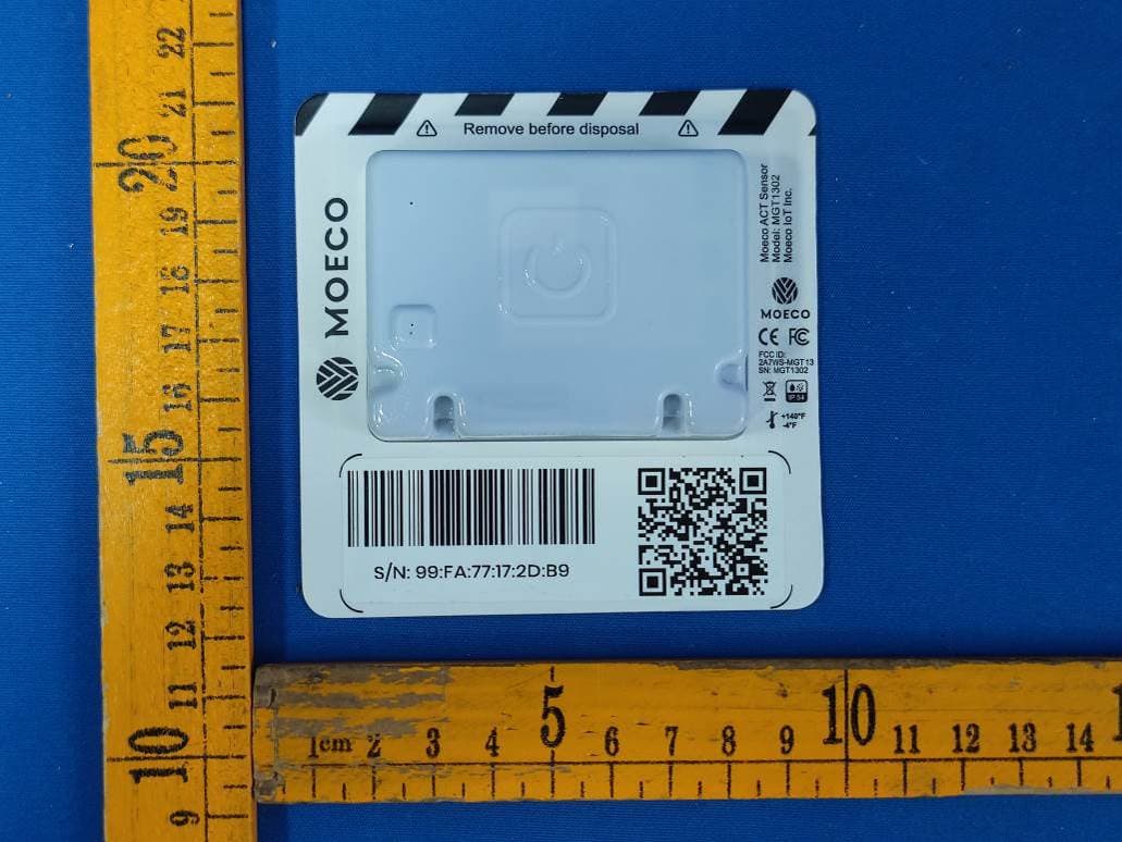
2A7WS-MGT1302
Jun 25, 2023Moeco ACT Sensor
Equipment Class
DTS - Digital Transmission System