2A88K-PLE52BLE Module
Ltech Inc.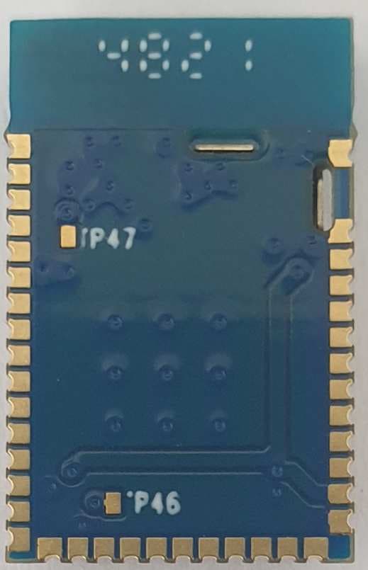
Click to zoom
Application Details
- Equipment Class
- DTS - Digital Transmission System
- Date of Grant
- Feb 01, 2023
- Application Purpose
- Original Equipment
- Date of Application
- Feb 01, 2023
- Equipment Note
- BLE Module
- Frequency Range
- 2402.00000000 - 2480.00000000
- Company
- Ltech Inc.
- Country
- South Korea
Documents & Files
Document Text
Text extracted from the exhibit documents filed with the FCC. Open a document above to read the original.
Users Manual
FCC ID : 2A88K-PLE52 Certification -KC FCC compliance information FCC ID : 2A88K-PLE52 Caution: Any changes or modifications in construction of this device which are not expressly approved by the responsible for compliance could void the user's authority to operate the equipment. NOTE: This device complies with Part 15 of the FCC Rules. Operation is subject to the following two conditions; 1. This device may not cause harmful interface, and 2. This device must accept any interference received, including interference that may cause undesired operation. This equipment has been tested and found to comply with the limits for a Class B Digital Device, pursuant to Part 15 of the FCC Rules. These limits are designed to this equipment generates, uses, and can radiate radio frequency energy and, if not installed and used in accordance with the instructions, may cause harmful interference to radio communications. However, there is no guarantee that interference will not occur in a particular installation. If this equipment does cause harmful interference to radio or television reception, which can be determined by turning the radio or television off and on, the user is encouraged to try to correct interference by one or more of the following measures. 1. Reorient or relocate the receiving antenna. 2. Increase the separation between the equipment and receiver. 3. Connect the equipment into an outlet on another circuit. 4. Consult the dealer or an experienced radio/TV technician for help. FCC Radiation Exposure Statement This equipment complies with FCC radiation exposure limits set forth for an uncontrolled environment. This equipment should be installed and operated with minimum distance 20cm between the radiator & your body. This module is intended for OEM integrator. The OEM intergrator is still responsible for the FCC compliance requirement of the end product, which integrates this module. Description of the product to which the module will be mounted The RF Module, PLE-52 , FCCID: 2A88 K-PLE52 will be installed on board of the NB -WC2 by NearBeBe.
Attestation Statements
Rev 1/26/2023 Ltech Inc. Federal Communications Commission Authorization and Evaluation Division 7435 Oakland Mills Road Columbia, MD 21046 USA Date: 01-31-2023 Ref: Attestation Statements Part 2.911(d)(7) Filing FCC ID: 2A88K-PLE52 [Ltech Inc.] (“the applicant”) certifies that, as of the date of the filing of the application, TIMCO Engineering, Inc. is our designated U.S. agent for service of process for the above referenced FCC ID. [Ltech Inc.] accepts to maintain an agent for no less than one year after the grantee has terminated all marketing and importation or the conclusion of any Commission-related proceeding involving the equipment. TIMCO Engineering, Inc. accepts, as of the date of the filing of the application, the obligation of the designated U.S. agent for service of process for the above referenced FCC ID. Designated U.S. Agent Information: Name: TIMCO Engineering, Inc. Address: 849 NW State Road 45, Newberry FL 32669 Contact Person: Bruno Clavier Tel.: 352-472-5500 Email: [email protected] Sincerely, Ltech Inc. TIMCO Engineering, Inc. Lee Seungmun Bruno Clavier
Attestation Statements
Rev 1/26/2023 Ltech Inc. Federal Communications Commission Authorization and Evaluation Division 7435 Oakland Mills Road Columbia, MD 21046 USA Date: 01-31-2023 Ref: Attestation Statements Part 2.911(d)(5)(i) Filing FCC ID: 2A88K-PLE52 [Ltech Inc.] (“the applicant”) certifies that the equipment for which authorization is sought is not “covered” equipment prohibited from receiving an equipment authorization pursuant to section 2.903 of the FCC rules. Sincerely, (Applicant signature) (Applicant printed name) Lee Seungmun Rev 1/26/2023 Ltech Inc. Federal Communications Commission Authorization and Evaluation Division 7435 Oakland Mills Road Columbia, MD 21046 USA Date: 01-31-2023 Ref: Attestation Statements Part 2.911(d)(5)(ii) Filing FCC ID: 2A88K-PLE52 [Ltech Inc.] (“the applicant”) certifies that, as of the date of the filing of the application, the applicant is not identified on the Covered List as an entity producing “covered” equipment. Sincerely, (Applicant signature) (Applicant printed name) Lee Seungmun
Cover Letter(s)
Ltech Inc. Elproma Elektronika Sp. z o.o Rev 11/20/07 Federal Communications Commission Authorization and Evaluation Division Confidentiality Request regarding application for certification of FCC ID: 2A88K-PLE52 Pursuant to Sections 0.457 and 0.459 of the Commission’s Rules, we hereby request confidential treatment of information accompanying this application as outlined below: Exhibit Type File Name Block Diagram PLE-52_Blk.pdf Part list PLE-52_Plist.pdf Schematics PLE-52_Schem.pdf Operational Description PLE-52_OpDesc.pdf The above materials contain trade secrets and proprietary information not customarily released to the public. The public disclosure of these materials may be harmful to the applicant and provide unjustified benefits to its competitors. The applicant understands that pursuant to Section 0.457 of the Rules, disclosure of this application and all accompanying documentation will not be made before the date of the Grant for this application. In additional to above mentioned documents, in order to comply with the marketing regulations in Title 47 CFR §2.803 and the importation rules in Title 47 CFR §2.1204, while ensuring that business sensitive information remains confidential until the actual marketing of newly authorized devices, we request Short Term Confidentiality of the following attachment(s); Exhibit Type File Name External Photo PLE-52_Ext Photos.pdf Internal Photo PLE-52_Int Photos.pdf Manual PLE-52_Manual.pdf Test Set-up Photo PLE-52_Tsup Photos.pdf For 45 days, pursuant to Public Notice DA 04-1705. OR For 180 days pursuant to KDB 726920 D01. Sincerely, Seungmun Lee / Team Leader
Cover Letter(s)
(Ltech Inc.) Date: 04/17/2018 VCB_F-01: Operating Procedures Form – FCC Modular v02 Page 1 of 1 MODULAR APPROVAL LETTER (PLE-52) FCC ID : 2A88K-PLE52, is seeking FCC Authorization as a Single Modular transmitter / Single Limited Modular Approval (Please check one) The EUT meets the requirements for Single Modular approval / Single Limited Modular Approval (please check one) as detailed in KDB 996369. Compliance to each of the requirements is described below: Modular Approval Requirement Yes No Please provide a detailed explanation if the answer is “No.” (i) The radio elements of the modular transmitter must have their own shielding. The physical crystal and tuning capacitors may be located external to the shielded radio elements. X (ii) The modular transmitter must have buffered modulation/data inputs (if such inputs are provided) to ensure that the module will comply with part 15 requirements under conditions of excessive data rates or over-modulation. X (iii) The modular transmitter must have its own power supply regulation. X (iv) The modular transmitter must comply with the antenna and transmission system requirements of §§ 15.203, 15.204(b) and 15.204(c). The antenna must either be permanently attached or employ a ‘‘unique’’ antenna coupler (at all connections between the module and the antenna, including the cable). The ‘‘professional installation’’ provision of § 15.203 is not applicable to modules but can apply to limited modular approvals under paragraph (b) of this section. X (v) The modular transmitter must be tested in a stand-alone configuration X (vi) The modular transmitter must be equipped with either a permanently affixed label or must be capable of electronically displaying its FCC identification number. X (vii) The modular transmitter must comply with any specific rules or operating requirements that ordinarily apply to a complete transmitter and the manufacturer must provide adequate instructions along with the module to explain any such requirements. A copy of these instructions must be included in the application for equipment authorization. X (viii) The modular transmitter must comply with any applicable RF exposure requirements in its final configuration. X Client’s signature: Client’s name & title: Seungmun Lee / Team Leader Contact information / address: +82-2-2619-9662 / RM.528.5FL, 229, Yangji-ro, Bucheon-si, Gyonggi-do, S. Korea
External Photos
Exterior Photographs Front Top Rear Bottom
ID Label/Location Info
PLE-52 Module Location: Top of Shield Cover PLE-52 FCCID:2A88K-PLE52 L-Ltech.com
Internal Photos
Interior Photographs Interior Main Board - Front Top Main Board(Open Shield) - Front Top Main board - Rear Bottom Chip Antenna
RF Exposure Info
페이지(page) : ( 2 )/( 총(Total) 7 ) ICRT-QPA-17-03 Rev.2 Report No. ICRT-TR-E223288-0A Contents 1. Applicant & Manufacturer & Test Laboratory Information .................................................................................. 4 1.1 Applicant information ........................................................................................................................................ 4 1.2 Manufacturer Information ................................................................................................................................. 4 1.3 Test Laboratory Information ............................................................................................................................ 4 2. Equipment under Test(EUT) Information ................................................................................................................. 5 2.1 General Information ........................................................................................................................................... 5 2.2 Additional Information ...................................................................................................................................... 5 2.3 Mode of operation during the test .................................................................................................................. 5 2.4 Modifications of EUT ......................................................................................................................................... 5 3. Maximum Permissible Exposure ............................................................................................................................... 6 3.1 RF Exposure calculation .................................................................................................................................. 6 3.1 Result ..................................................................................................................................................................... 7 페이지(page) : ( 3 )/( 총(Total) 7 ) ICRT-QPA-17-03 Rev.2 Report No. ICRT-TR-E223288-0A Revision History Issued Report No. Issued Date Revisions Effect Section ICRT-TR-E223288-0A 2022.12.14 Initial Issue All 페이지(page) : ( 4 )/( 총(Total) 7 ) ICRT-QPA-17-03 Rev.2 Report No. ICRT-TR-E223288-0A 1. Applicant & Manufacturer & Test Laboratory Information 1.1 Applicant information Applicant Ltech Inc. Address RM.528.5FL, 229, Yangji-ro, Bucheon-si, Gyonggi-do, S. Korea Contact Person Seungmun Lee Telephone No. +82-2-2619-9662 Fax No. - E-mail [email protected] 1.2 Manufacturer Information Manufacturer Ltech Inc. Address RM.528.5FL, 229, Yangji-ro, Bucheon-si, Gyonggi-do, S. Korea 1.3 Test Laboratory Information Conducted tests were performed at Laboratory ICR Co., Ltd. Address 112, Hwanggeum 3-ro 7beon-gil, Hagun-ri, Yangchon-eup, Gimpo-si, Gyeonggi- do, Korea Telephone No. +82-2-6351-9002 Fax No. +82-2-6351-9007 RRA No. KR0165 KOLAS No. KT652 페이지(page) : ( 5 )/( 총(Total) 7 ) ICRT-QPA-17-03 Rev.2 Report No. ICRT-TR-E223288-0A 2. Equipment under Test(EUT) Information 2.1 General Information Product Name BLE Module Brand Name - Model Name PLE-52 Additional Model Name - FCC ID 2A88K-PLE52 2.2 Additional Information Equipment Class DTS - Digital Transmission System Device Type Stand-alone Operating Frequency Bluetooth LE (1/2 Mbps) 2 402 MHz ~ 2 480 MHz RF Output Power Bluetooth LE (1/2 Mbps) 1 Mbps -5.61 ㏈m 2 Mbps -5.62 ㏈m Number of Channel Bluetooth LE (1/2 Mbps) 40 Modulation Type GFSK Antenna Type Chip Antenna Antenna Gain 0.5 ㏈i Antenna Operating Mode Single Antenna Equipment with only one antenna 2.3 Mode of operation during the test - The EUT is continuous transmission mode during the test with set at Low Channel, Middle Channel, and High Channel. To get a maximum radiated emission levels from the EUT, the EUT was moved throughout the XY, YZ, XZ planes. 2.4 Modifications of EUT - None 페이지(page) : ( 6 )/( 총(Total) 7 ) ICRT-QPA-17-03 Rev.2 Report No. ICRT-TR-E223288-0A 3. Maximum Permissible Exposure 3.1 RF Exposure calculation According to the FCC rule 1.1310 table 1B, the limit for the maximum permissible RF exposure for an uncontrolled environment are f/1500 ㎽/㎝² for the frequency range between 300 ㎒ and 1 500 ㎒ and 1.0 ㎽/㎝² for the frequency range between 1 500 ㎒ and 100 000 ㎒. The electric field generated for a 1 ㎽/㎝² exposure is calculated as follows: E = √ (30 * P * G) / d, and S = E² / Z = E² / 377, because 1 ㎽/㎝² = 10 W/m² Where S = Power density in ㎽/㎝², Z = Impedance of free space, 377 Ω E = Electric filed strength in V/m, G = Numeric antenna gain, and d = distance in meter Combing equations and rearranging the terms to express the distance as a function of the remaining variable d = √ (30 * P * G) / (377 *10 S) Changing to units of ㎽ and cm, using P (㎽) = P (W) / 1 000, d (㎝) = 0.01 * d (m) d = 0.282 * √ (P * G) / S Where d = distance in ㎝, P = Power in ㎽, G = Numeric antenna gain, and S = Power density in ㎽/㎝² 페이지(page) : ( 7 )/( 총(Total) 7 ) ICRT-QPA-17-03 Rev.2 Report No. ICRT-TR-E223288-0A 3.1 Result According to above equation, the following result was obtained. Operating Mode Target Power W / tolerance Max tune up power Antenna Gain Power Density (㎽/㎝²) @ 20 ㎝ Separation Limit (㎽/㎝²) (㏈m) (㎽) Log Linear Bluetooth LE (1 Mbps) -5.61 ± 1.0 -4.61 0.35 0.50 1.12 0.000 1 1.00 Bluetooth LE (2 Mbps) -5.62 ± 1.0 -4.62 0.35 0.50 1.12 0.000 1 For getting power density at 20 ㎝ separation in above table, following formula was used. S = P * G / (4π * R²) = 0.35 * 1.12/ (4 * π * 20^2) = 0.000 1 Where: S = Power Density, P = Power input to the external antenna (Output power from the EUT antenna port (㏈m) – cable loss (㏈)), G = Gain of Transmit Antenna (linear gain), R = Distance from Transmitting Antenna - END -
Test Report
2450 MHz AntennaP/N 2450AT18B100 Detail Specification: 08/10/09 Page 1 of 3 General Specifications Part Number 2450AT18B100 Input Power 3W max. Frequency Range 2400 - 2500 Mhz Impedance 50 Ω Peak Gain 0.5 dBi typ. (XZ-V) Operating Temperature -40 to +85°C Average Gain -0.5 dBi typ. (XZ-V) Reel Quanity 3,000 Return Loss 9.5 dB min. Terminal Configuration Packaging BulkSuffix = SEg. 2450AT18B100S No. Function P/N Style T & RSuffix = EEg. 2450AT18B100E 1 Feeding Point Suffix Termination 100% TinSuffix = None Eg. 2450AT18B100(E or S) 2 NC Style Tin / Lead Mechanical Dimensions Inmm L ±± W ±± T a ±± Mounting Considerations Mount these devices with brown mark facing up. Units: mm Line width should be designed to provide 50 Ω impedance matching characteristics. a) Without Matching Circuits b) With Matching Circuits Johanson Technology, Inc. reserves the right to make design changes without notice. All sales are subject to Johanson Technology, Inc. terms and conditions. www.johansontechnology.com 4001 Calle Tecate • Camarillo, CA 93012 • TEL 805.389.1166 FAX 805.389.1821 2009 Johanson Technology, Inc. All Rights Reserved Please consult Factory 0.0120.020 1.30 0.30 1.600.200.008 0.051 +.004/-.008+0.1/-0.2 "High Frequency Ceramic Solutions" 0.50 0.1260.0083.200.20 0.063 1 2 L W a T ) Matching Component JTI P/Ns: L-14C2N7JV4 L-14C2N2JV4 * 2.6 4.2 1.6 1.9 0.4 2.7nH 1.2pF 3.3nH JTI P/N for Matching Circuit: Cap (1.2pF): 500R07S1R2BV4T Inductor (2.7nH): L-07C2N7SV6T Inductor (3.3nH): L-07C3N3SV6T 2450 MHz AntennaP/N 2450AT18B100 Detail Specification: 08/10/09 Page 2 of 3 Typical Electrical Characteristics (T=25 o C) Test Board: Return Loss a) Without Matching Circuitb) With Matching Circuit Johanson Technology, Inc. reserves the right to make design changes without notice. All sales are subject to Johanson Technology, Inc. terms and conditions. www.johansontechnology.com 4001 Calle Tecate • Camarillo, CA 93012 • TEL 805.389.1166 FAX 805.389.1821 2009 Johanson Technology, Inc. All Rights Reserved "High Frequency Ceramic Solutions" ) ) ) ) ) ) ) ) ) Ground 13.5mm 6.5mm 39.5mm 6.5mm Matching Circuit No Ground 50Ω Feed Line Antenna 19mm 4mm 2450 MHz AntennaP/N 2450AT18B100 Detail Specification: 08/10/09 Page 3 of 3 Typical Radiation Patterns Johanson Technology, Inc. reserves the right to make design changes without notice. All sales are subject to Johanson Technology, Inc. terms and conditions. www.johansontechnology.com 4001 Calle Tecate • Camarillo, CA 93012 • TEL 805.389.1166 FAX 805.389.1821 2009 Johanson Technology, Inc. All Rights Reserved "High Frequency Ceramic Solutions" ) ) ) ) ) ) ) ) ) Mouser Electronics Authorized Distributor Click to View Pricing, Inventory, Delivery & Lifecycle Information: Johanson: 2450AT18B100E
Test Report
페이지(page) : ( 2 )/( 총(Total) 41 ) ICRT-QPA-17-03 Rev.2 Report No. ICRT-TR-E223287-0A Contents 1. Applicant & Manufacturer & Test Laboratory Information .................................................................................. 4 1.1 Applicant information ........................................................................................................................................ 4 1.2 Manufacturer Information ................................................................................................................................. 4 1.3 Test Laboratory Information ............................................................................................................................ 4 2. Equipment under Test(EUT) Information ................................................................................................................. 5 2.1 General Information ........................................................................................................................................... 5 2.2 Additional Information ...................................................................................................................................... 5 2.3 Mode of operation during the test .................................................................................................................. 5 2.4 Modifications of EUT ......................................................................................................................................... 5 3. Test Summary ................................................................................................................................................................. 6 3.1 Test standards and results .............................................................................................................................. 6 3.2 Purpose of the test ............................................................................................................................................. 6 3.3 Test Methodology ............................................................................................................................................... 6 3.4 Configuration of Test System ......................................................................................................................... 6 3.5 Antenna requirement ......................................................................................................................................... 7 4. Used equipment on test ............................................................................................................................................... 8 5. 6 ㏈ ㏈㏈ ㏈ Bandwidth .............................................................................................................................................................. 9 5.1 Operating environment ..................................................................................................................................... 9 5.2 Measurement method ........................................................................................................................................ 9 5.3 Test data ............................................................................................................................................................... 9 6. Maximum Conducted Output Power ....................................................................................................................... 14 6.1 Operating environment ................................................................................................................................... 14 6.2 Measurement method ...................................................................................................................................... 14 6.3 Test data ............................................................................................................................................................. 14 7. Power Spectral Density .............................................................................................................................................. 15 7.1 Operating environment ................................................................................................................................... 15 7.2 Measurement method ...................................................................................................................................... 15 7.3 Test data ............................................................................................................................................................. 15 8. Conducted Spurious Emission ................................................................................................................................ 20 8.1 Operating environment ................................................................................................................................... 20 8.2 Measurement method ...................................................................................................................................... 20 8.3 Test data ............................................................................................................................................................. 20 9. Radiated Spurious Emission .................................................................................................................................... 30 9.1 Operating environment ................................................................................................................................... 30 9.2 Measurement method ...................................................................................................................................... 30 9.3 Test setup ......................................................................................................................................…
Text truncated - open the document above for the full version.
Test Setup Photos
페이지(page) : ( 1 )/( 총 2 ) ICRT-QP-22-02 Rev.5 Report No. ICRT-TR-E223287-0A Test Setup Photo Test Setup Radiated measurement for below 1 ㎓ (Front side) Test Setup Radiated measurement for below 1 ㎓ (Rear side) 페이지(page) : ( 2 )/( 총 2 ) ICRT-QP-22-02 Rev.5 Report No. ICRT-TR-E223287-0A Test Setup Radiated measurement for Above 1 ㎓ (Front side) Test Setup Radiated measurement for Above 1 ㎓ (Rear side)
Contact Information
Applicant
Seungmun Lee
Test Firm
ICR Co., Ltd.Sim Sang-Woo
Technical Specifications
| # | Rule Parts | Frequency Range | Power Output |
|---|---|---|---|
| 1 | 15C | 2.40 GHz - 2.48 GHz | 275.00 µW |