2A8AKQC610-410EVKVVDN_QCS610_410_EVK
VVDN Technologies Private Limited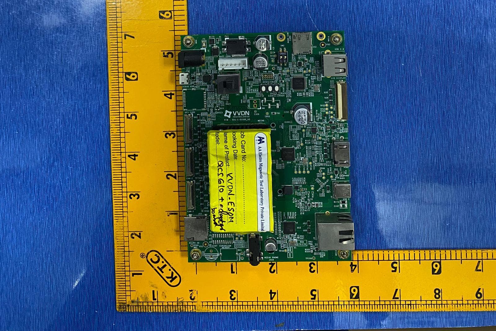
Click to zoom
Application Details
- Equipment Class
- NII - Unlicensed National Information Infrastructure TX
- Date of Grant
- Nov 06, 2022
- Application Purpose
- Original Equipment
- Date of Application
- Nov 06, 2022
- Equipment Note
- VVDN_QCS610_410_EVK
- Frequency Range
- 5745.00000000 - 5825.00000000
- Country
- India
Documents & Files
Document Text
Text extracted from the exhibit documents filed with the FCC. Open a document above to read the original.
Users Manual
VVDN_ESOM 8-07-2022 VVDN QCS 610 EVK User Guide VVDN_QCS610 Development Board User Guide A0-06 2 CONFIDENTIAL Revision History: DATE REVISION NO. DESCRIPTION BY 29-10-2021 A0-01 Initial release VVD N 08-11-2021 A0-02 Added Mini PCIe & Expansion HDR details VVD N 16-03-2022 A0-03 Added performance validation of interfaces VVD N 23-03-2022 A0-04 Internal review comments updated VVD N 28-06-2022 A0-05 Camera section added VVD N 8-07-2022 A0-06 Internal review comments updated VVD N VVDN_QCS610 Development Board User Guide A0-06 3 CONFIDENTIAL Table of Contents 1. Introduction 5 2. QCS610 + Carrier Board 5 2.1 Power Source Selection 6 3. Debug Console (Micro B) 6 4. USB 3.1 Type -C 7 5. UART Console setup 7 6. Powering up the system 9 7. ADB setup:- 11 8. DC Power Jack Details 12 9. QDL & FASTBOOT Flashing Guide (Linux) 13 10. Expansion Header details (H7) 17 11. Mini PCIe Connector Details (J11) 18 12. Performance validation of interfaces 19 12.1 Ethernet 19 12.2 Wi-Fi 20 12.3 Bluetooth 23 12.4 IMX462 Camera Board Connection to QCS610 EVK 25 12.4.1. Prerequisites 26 12.4.2. Steps for validating camera sensor - Using Recording pipeline 26 12.4.3. Steps for validating camera sensor - Using streaming pipeline 27 12.4.3.1. Streaming over USB 27 12.4.3.2. Streaming over Network 28 12.4.3.3. Streaming over HDMI Display 30 13. Interface Validation Summary 32 13.1 Ongoing developments 32 13.2 Known bugs 32 List of Figures 1. Introduction 5 2. QCS610 + Carrier Board 5 2.1 Power Source Selection 6 3. Debug Console (Micro B) 6 4. USB 3.1 Type -C 7 5. UART Console setup 7 VVDN_QCS610 Development Board User Guide A0-06 4 CONFIDENTIAL 6. Powering up the system 9 7. ADB setup:- 11 8. DC Power Jack Details 12 9. QDL & FASTBOOT Flashing Guide (Linux) 13 10. Expansion Header details (H7) 17 11. Mini PCIe Connector Details (J11) 18 12. Performance validation of interfaces 19 12.1 Ethernet 19 12.2 Wi-Fi 20 12.3 Bluetooth 23 12.4 IMX462 Camera Board Connection to QCS610 EVK 25 12.4.1. Prerequisites 26 12.4.2. Steps for validating camera sensor - Using Recording pipeline 26 12.4.3. Steps for validating camera sensor - Using streaming pipeline 27 12.4.3.1. Streaming over USB 27 12.4.3.2. Streaming over Network 28 12.4.3.3. Streaming over HDMI Display 30 13. Interface Validation Summary 32 13.1 Ongoing developments 32 13.2 Known bugs 32 VVDN_QCS610 Development Board User Guide A0-06 5 CONFIDENTIAL 1. Introduction This document contains information about the powering-up steps required for the VVDN QCS610 development board. 2. QCS610 + Carrier Board A 12V DC adaptor is required to power the QCS610 development board (minimum 1A current is required) Figure 1: QCS610 SOM + Carrier Board VVDN_QCS610 Development Board User Guide A0-06 6 CONFIDENTIAL 2.1 Power Source Selection Below figures shows the switch position options for DC Power and Battery Power selection. Figure 2: Position of Switch Figure 3: Positioning of Switch (SW2) 3. Debug Console (Micro B) Connect USB Micro -B cable to the J13 port of the board and PC to get the UART console. VVDN_QCS610 Development Board User Guide A0-06 7 CONFIDENTIAL 4. USB 3.1 Type -C Figure 4: Micro-B (J13) Connect Type -C cable to the USB 3.1 Type C port of the board and PC to get adb console. Figure 5: USB 3.1 Type-C (J9) 5. UART Console setup UART Console can be obtained either using minicom or picocom. Using minicom- ● Run “minicom -s” in the PC and make the minicom settings from “Serial port setup” option. Refer the image attached below: VVDN_QCS610 Development Board User Guide A0-06 8 CONFIDENTIAL Figure 6: Console settings in minicom ● After making the proper settings run the command “minicom -D /dev/tty<device_node>” in the laptop to get the board console. For example : minicom -D /dev/ttyUSB0 Check the print by running the command “dmesg | grep tty | tail -1” as shown below Using picocom- ● Use the command “picocom -b 115200 /dev/tty<device_node>” in the laptop to get the board console. For example : picocom -b 115200 /dev/ttyUSB0. Figure 7: Console settings in picocom VVDN_QCS610 Development Board User Guide A0-06 9 CONFIDENTIAL 6. Powering up the system Below are the steps needed for setting up the system 1. USB 3.1 type-C cable, connect the board and PC for ADB shell 2. Micro-B cable, connect the board and PC for Debug Console 3. 12V DC adapter to the DC jack for Power 4. Once the Red LED (D67) is ON ,Press the Phone ON button (SW4) (QCS610 has multiple power On events like USB In , CBL_PWR# etc... depends on that the board may auto power On ) Figure 8: Connections ● Press the phone ON switch shown below to power on QCS610 SOM board or by simply connecting the type-C cable itself the SOM board will power ON. VVDN_QCS610 Development Board User Guide A0-06 10 CONFIDENTIAL Figure 9: Phone ON Switch ● After powering the SOM board , booting starts and the booting logs can be seen in picocom/minicom terminal. Figure 10: Logs - Booting After booting at the login screen, enter “root” as the username and “oelinux123” as password .The image below shows the obtained console and login screen. VVDN_QCS610 Development Board User Guide A0-06 11 CONFIDENTIAL 7. ADB setup:- Figure 11: Console and Login Screen Connect the USB 3.1 Type C cable, wait for few seconds after the boot up and then open the terminal and enter the below commands for getting into adb shell. 1. adb root 2. adb shell The figure below show the obtained terminal and login Figure 12: Terminal showing ADB VVDN_QCS610 Development Board User Guide A0-06 12 CONFIDENTIAL 8. DC Power Jack Details Manufacturer: - CHUFON TECHNOLOGY CO., LTD (C-TEK) Part Number: - C020083-02 Dimensions are in mm Figure 13: DC Power Jack Details VVDN_QCS610 Development Board User Guide A0-06 13 CONFIDENTIAL 9. QDL & FASTBOOT Flashing Guide (Linux) The QCS610 Device can be flashed using QFIL (initial full flashing) or using Fastboot. 9.1 QDL Flashing Steps (Linux):- 1. Install below packages ○ sudo apt-get install libxml2-dev libudev-dev 2. Clone …
Text truncated - open the document above for the full version.
Cover Letter(s)
FCC Software Configuration Control Declaration Date: October 20, 2022 Federal Communications Commission 7435 Oakland Mills Road Columbia, MD 21046 USA Attn: OET Dept. Product/ Model Number: QCS610 EVK (SOM + Carrier) Regarding FCC Country Code Selection guidelines identified in KDB 594280. “All applications for equipment authorization for transmitters that can have radio parameters, or other technical parameters, reported to the Commission set by software must have an attestation indicating that no third party will have software, or configuration control, to program the device out of compliance of the technical rules under which it has been certified.” We declare that no third party will have software, or configuration control, to program the device out of compliance of the technical rules under which it has been certified.
Cover Letter(s)
Agent Authorization Company: VVDN Technologies Private Limited Address: 29975 Technology Drive, Suite 101 Murrieta, CA 92563 Product Name: QCS610-410EVK Model Number(s): QCS610 EVK (SOM + Carrier) Product Description: This is an evaluation board (SOM +Carrier) based on Qualcomm 610/410 processor. The Qualcomm® QCS610/410 SoC is a high performance loT System- on-Chip (SoCs) delivering premium features for building advanced smart camera and loT use cases encompassing machine learning, edge computing, sensor processing, voice UI enablement and integrated wireless connectivity cost effectively. This evaluation board will help developers to develop and test their on applications before actual product design. Also it will help to evaluate the performance of QCS610/410 processor. We authorize MiCOM Labs Inc., 575 Boulder Court, Pleasanton, California 94566, USA, to act on our behalf on all matters concerning the certification of above named equipment. We declare that MiCOM Labs Inc. is allowed to forward all information related to the approval and certification of equipment to the regulatory agencies as required and to discuss any issues concerning the approval application. Any and all acts carried out by MiCOM Labs on our behalf shall have the same effect as acts of our own.
Cover Letter(s)
Office of Engineering Technology Federal Communications Commission 7435 Oakland Mills Road Columbia, MD 21046 Subject: Request for Confidentiality FCC ID: 2AZOIION4L3 To Whom It May Concern, Pursuant to the provisions of Sections 0.457 and 0.459 of Commission's rules (47CFR0.457, 0.459), we are requesting the Commission to withhold the following attachment(s) as confidential document from public disclosure. Exhibits Long-Term Confidentiality Short-Term Confidentiality NOTE 2 ID Label/Location No No Attestation Statement No No External Photos No ☒ Block Diagram ☒ ☐ Schematics ☒ ☐ Test Report No No Test Setup Photos No ☒ User’s Manual ☐ NOTE 1 ☒ Internal Photos ☐ NOTE 1 ☒ Parts List ☒ ☐ RF Exposure Info No No Operational Description ☒ ☐ Cover Letter(s) No No SDR Software / Security Info ☒ No NOTE 1: Long-Term Confidentiality may be permitted under special conditions (See II. LONG-TERM CONFIDENTIALITY, Section 3 of KDB 726920, use last in force) NOTE 2: Short-Term Confidentiality can be requested for a maximum of 180 days from the date of the grant. Above mentioned document contains detailed system and equipment description are considered as proprietary information in operation of the equipment. The public disclosure of above documents might be harmful to our company and would give competitor an unfair advantage in the market. In case of short-term Confidentiality, the applicant requests the exhibits selected above are withheld from public view for a period of ___180__ days from the date of the Grant of Equipment Authorization and prior to marketing. It is our understanding that all measurement test reports, FCC ID label format and correspondent during certification review process cannot be granted as confidential documents and those information will be available for public review once the grant of equipment authorization is issued.
Cover Letter(s)
©VVDN Technologies 2020 | Confidentialwww.vvdntech.com -1- www.vvdntech.com © VVDN Technologies 2020 | Confidential Premier Electronics Engineering & Manufacturing Company Creating Opportunities & Transforming Lives Comparison between 410 and 610 SOM 04-Aug-2022 ©VVDN Technologies 2020 | Confidentialwww.vvdntech.com -2- VVDN-QLCM-410/610EVK •VVDN-QCS-EVK board supports following SOM modules, 1. QCS 410 SOM 2. QCS 610 SOM •The major difference between the two SOMs are that it uses two different Qualcomm processors i.eQCS 410 and QCS 610. And compared to QCS410 ,QCS610 is having more processing power. •Although the processors used are different, other chipsets/subsystems used in the SOM are same. 1. PMIC-PM6150 & PM6150L for power management 2. 16GB eMMCfor storage. 3. Qualcomm WCN3980 for Wi-Fi & Bluetooth 4. 4GB LPDDR4x as Memory SOM Board Carrier Board ©VVDN Technologies 2020 | Confidentialwww.vvdntech.com -3- QCS 410/610 SOM BLOCK DIAGRAM QCS 410 SOMQCS 610 SOM ●The major difference is on Qualcomm Processor chipset. ©VVDN Technologies 2020 | Confidentialwww.vvdntech.com -4- Comparison between QCS 410 and QCS 610 Processor based SOM Technical Specifications QCS 410 SOM QCS 610 SOM ●Processor Qualcomm QCS410 ●Processor-KryoGold: Dual high-performance cores up to 2.2 GHz , KryoSilver: Dual low-power cores up to 1.8 GHz It supports Multi-format codec up to 1080p90 video encode. Multi-stream codec (1080p30 (H.264)+ 1080p30 (YUV) + 480P (VA -YUV)) •All other blocks inthe QCS410/610 processor are same and both are pin to pin compatible ●Processor Qualcomm QCS610 ●Processor-KryoGold: Dual high-performance cores up to 2.2 GHz, KryoSilver: Hexalow-power cores up to 1.8 GHz It supports Multi-format codec up to 4K30 video encode. Multi-stream codec (4K30 (HEVC) + 720p30 (YUV) + 480p30 (VA -YUV)) •All other blocks inthe QCS410/610 processor are same and both are pin to pin compatible ●PM6150 -Qualcomm PMIC ●PM6150L -Qualcomm master PMIC ●PM6150 -Qualcomm PMIC ●PM6150L -Qualcomm master PMIC ●4GB LPDDR4X Memory Kingston memory-B3221XC5GDGUKR ●4GB LPDDR4X Memory Samsung memory-K4UBE3D4AA-MGCL ●16GB eMMC-Kingston●16GB eMMC-Kingston ●Wi-Fi 2.4GHz/5GHz -Qualcomm WCN3980●Wi-Fi 2.4GHz/5GHz -Qualcomm WCN3980 ●Bluetooth -Qualcomm WCN3980●Bluetooth -Qualcomm WCN3980 ©VVDN Technologies 2020 | Confidentialwww.vvdntech.com -5- Compactibility ●Both 410 and 610 processor based SOMs are compactible with this carrier board QCS 410 SOM QCS 610 SOM Carrier Board ©VVDN Technologies 2020 | Confidentialwww.vvdntech.com -6- CREATE. INNOVATE. PRODUCE #WEMAKEITHAPPEN Premier Electronics Engineering & Manufacturing Company /vvdn-technologies /vvdn-technologies /vvdn-technologies /vvdn-technologies www.vvdntech.com
Internal Photos
Antenna Port Antenna Port
RF Exposure Info
RF EXPOSURE EVALUATION 1.PRODUCTINFORMATION Product Description QCS610-410EVK Model Name QCS610 EVK (SOM + Carrier) FCC ID 2A8AKQC610-410EVK 2.EVALUATION METHODANDLIMIT Human exposure to RF emissions from mobile devices(47CFR§2.1091) may be evaluated based on the MPE limits adopted by the FCC for electric and magnetic field strength and/or power density, as appropriate, since exposures are assumed to occur at distances of 20 cm or more from persons. LIMITS FOR GENERAL POPULATIONIUNCONTROLLED EXPOSURE Frequency Range (MHz) E-field Strength (E) (V/m) Magnetic Field Strength (H) (A/m) Power Density(S) (mW/cm 2 ) Averaging Time IEl 2 IHl 2 or , S(Minutes) 0.3--1.34 614 1.63 (100)* 30 1.34--30 824/f 2.19/f (180/f 2 )* 30 30--300 27.5 0.073 0.2 30 300--1500 -- -- f/1500 30 1500--100,000 -- -- 1.0 30 *Note: 1.f= Frequency in MHz*Plane-wave Equivalent Power Density 2.The averaging time for General Population/Uncontrolled exposure to fixed transmitters is not applicable for mobile and portable transmitters. (operated in BT/ WIFI) See47CFR§§2.1091 and 2.1093 on source-based time-averaging requirement for mobile and portable transmitters. S=PG/4rrR 2 Where: S=power density P=power input toantenna G=power gain of the antenna in the direction of interest relative to anisotropic radiator R=distance to the center of radiation of the antenna 3.CALCULATION A minimum test separation distance 20cm is required between the antenna and radiating structures of the device and nearby persons to apply mobile device exposure limits. The distance must be at least 20cm and fully supported by the operating and installation configurations of the transmitter and its antenna(s), according to the source-based time-averaged maximum power requirements of §2.1091(d)(2). In cases where cable losses or other attenuations are applied to determine compliance, the most conservative operating configurations and exposure conditions must be evaluated. Antenna Gain (2.4GHz (Wi-Fi, BLE, BT)) = 3.2dBi (Numeric = 2.089), rr = 3.14 Antenna Gain (5GHz) = 4.25dBi (Numeric = 2.661), rr = 3.14 Frequency (MHz) Output Power (dBm) Output Power (mW) Power Density (mW/cm 2) Power Density Limit (mW/cm 2) 2412 (Wi-Fi) 22.15 164.058 0.06821599 1 2440 (BLE) 6.87 4.864 0.002022471 1 2441 (BT) 10.43 11.040 0.004590477 1 5230 (Wi-Fi) Band 1 22.39 173.380 0.091832042 1 5745 (Wi-Fi) Band 4 22.84 192.309 0.101857931 1 Note: Only the worst case recorded.
Test Report
AA Electro Magnetic Test Laboratory Private Limited 1 | P a g e Plot No.174, UdyogVihar Phase 4, Sector -18, Gurgaon -122016, Haryana, India Contact: 0124-4235350, 4145343; e-mail: info @aaemtlabs.com; Website: www.aaemtlabs.com Report No.: AAEMT/EMC/220328-02-04 FCC RADIO TEST REPORT Part 15 subpart E FCC ID:2A8AKQC610-410EVK Report Reference No. ............................ : AAEMT/EMC/220328-02-04 Date of issue .......................................... : 2022-05-05 Testing Laboratory ................................ : AA Electro Magnetic Test Laboratory Private Limited Plot No 174, Udyog Vihar - Phase 4, Sector 18, Certificate#5593.01 Address.................................................. : Gurgaon, Haryana, India Applicant’s name................................... : VVDN Technologies Pvt. Ltd. Address.................................................. : 398, Sector 8, Imt Manesar, Gurugram, Haryana 122051. Manufacturer ......................................... : VVDN Technologies Pvt. Ltd. Address........................................: Test specification: 398, Sector 8, Imt Manesar, Gurugram, Haryana 122051 QCS610-410EVK Test item description ............................. : VVDN Trade Mark............................................ : Model/Type reference ......................... : QCS610 EVK (SOM+Carrier) Ratings................................................... : Input of EUT: Powered through Adapter Input for Meanwell adapter: 110-240VAC,50/60Hz,1.4A, Output: 12VDC,5A, 60W (max) Prepared By (+ signature) Ankur Kumar: Reviewed & Approved by: (+ signature) Dr. Lenin Raja (Authorized Representative) (/ lenin83/) AA Electro Magnetic Test Laboratory Private Limited 2 | P a g e Plot No.174, UdyogVihar Phase 4, Sector -18, Gurgaon -122016, Haryana, India Contact: 0124-4235350, 4145343; e-mail: info @aaemtlabs.com; Website: www.aaemtlabs.com Report No.: AAEMT/EMC/220328-02-04 Certificate#5593.01 TABLE OF CONTENTS 1. Summary of test results ........................................................................................................................ 5 2. General test information ...................................................................................................................... 6 2.1. Description of EUT .............................................................................................................................. 6 2.2. Accessories of EUT ............................................................................................................................. 7 2.3. Assistant equipment used for test ........................................................................................................ 8 3. Equipments List for All Test Items ...................................................................................................... 9 3.1. Block diagram of EUT configuration for test .................................................................................... 11 3.2. Test environment conditions .............................................................................................................. 11 3.3. Measurement uncertainty ................................................................................................................... 11 4. POWER SPECTRAL DENSITY TEST ............................................................................................ 12 4.1. Block diagram of test setup................................................................................................................ 12 4.2. Applied procedures / limit ................................................................................................................. 12 4.3. Test Procedure ................................................................................................................................... 13 4.4. Test Result ......................................................................................................................................... 14 5 26 dB & 99% Emission Bandwidth .................................................................................................................... 32 5.1 Block diagram of test setup ............................................................................................................................. 32 5.1 Applied procedures / limit ............................................................................................................................... 32 5.2. Test Procedure ................................................................................................................................... 32 5.3. Test Result ......................................................................................................................................... 33 6. MAXIMUM CONDUCTED OUTPUT POWER.............................................................................. 65 6.1. Test Result ......................................................................................................................................... 66 7 Band Edges Measurement .................................................................................................................................. 67 7.1. Test Result ......................................................................................................................................... 68 8. RADIATED EMISSION MEASUREMENT .................................................................................... 80 8.1. Block diagram of test setup................................................................................................................ 80 8.2. Limit .................................................................................................................................................. 82 8.3. Test Procedure ................................................................................................................................... 83 8.4. Test result(Belo…
Text truncated - open the document above for the full version.
Test Report
APPLICATION SPECIFICATION REVISION: ECR/ECN INFORMATION: TITLE: WIFI 6E FLEX CABLE BALANCE ANTENNA APPLICATION SPECIFICATION SHEET No. J EC No: 673961 1 of 30 DATE: 2021/08/17 DOCUMENT NUMBER: CREATED / REVISED BY: CHECKED BY: APPROVED BY: AS-1461530100 Liu Hai 2021/08/12 Andy Zhang 2021/08/12 Chris Zhong 2021/08/12 TEMPLATE FILENAME: APPLICATION_SPEC[SIZE_A](V.1).DOC TITLE WIFI 6E FLEX CABLE BALANCE ANTENNA TABLE OF CONTENTS 1.0 SCOPE 2.0 PRODUCT DESCRIPTION 3.0 APPLICABLE DOCUMENTS 4.0 ANTENNA PERFORMANCE 5.0 ASSEMBLY GUIDELINE 6.0 RF PERFORMANCE AS A FUNCTION OF IMPLEMENTATION 7.0 THE ANTENNA PERFORMANCE VARIATION WITH CABLE LENGTH 8.0 CHANGE HISTORY APPLICATION SPECIFICATION REVISION: ECR/ECN INFORMATION: TITLE: WIFI 6E FLEX CABLE BALANCE ANTENNA APPLICATION SPECIFICATION SHEET No. J EC No: 673961 2 of 30 DATE: 2021/08/17 DOCUMENT NUMBER: CREATED / REVISED BY: CHECKED BY: APPROVED BY: AS-1461530100 Liu Hai 2021/08/12 Andy Zhang 2021/08/12 Chris Zhong 2021/08/12 TEMPLATE FILENAME: APPLICATION_SPEC[SIZE_A](V.1).DOC WIFI 6E FLEX CABLE BALANCE ANTENNA 1.0 SCOPE This specification describes the antenna application and surrounding. The information in this document is for reference and benchmark purposes only. The user is responsible for validating antenna rf performance based on the user’s actual implementation. Antenna illustrations in this document are generic representations. They are not intended to be an image of any antenna listed in the scope. 2.0 PRODUCT DESCRIPTION 2.1 PRODUCT NAME AND SERIES NUMBER (S) Product name: WIFI 6E flex cable balance antenna Series Number: 146153 2.2 DESCRIPTION Series 146153 is a balanced, dipole-type, high efficiency antenna for 2.4/5/6 GHz applications, including WiFi 6E, Bluetooth, Zigbee and others. This antenna is made from poly flexible material with small size 35*9*0.1mm and has double-sided adhesive tape for easy “peel and stick” mounting. This balanced antenna with ground plane independent design offers various cable length options for ease of integration into various devices. 2.3 PRODUCT STRUCTURE INFORMATION Please refer to PS-1461530100 for full information. ANTENNA 3D VIEW APPLICATION SPECIFICATION REVISION: ECR/ECN INFORMATION: TITLE: WIFI 6E FLEX CABLE BALANCE ANTENNA APPLICATION SPECIFICATION SHEET No. J EC No: 673961 3 of 30 DATE: 2021/08/17 DOCUMENT NUMBER: CREATED / REVISED BY: CHECKED BY: APPROVED BY: AS-1461530100 Liu Hai 2021/08/12 Andy Zhang 2021/08/12 Chris Zhong 2021/08/12 TEMPLATE FILENAME: APPLICATION_SPEC[SIZE_A](V.1).DOC 3.0 APPLICABLE DOCUMENTS DOCUMENT NUMBER DESCRIPTION Sale Drawing (SD) SD-1461530050 Mechanical Dimension of the product SD-1461531050 Product Specification (PS) PS-1461530100 Product Specification Packing Drawing (PK) PK-1461530100 Product packaging specifications 4.0 ANTENNA PERFORMANCE 4.1 RF TEST CONDITIONS All measurements are done of the antenna mounted on a PC/ABS material block of 1.5mm thickness with VNA Agilent E5071C and Over-The-Air (OTA) chamber. All measurements in this document are done with the part no.1461530100 with a cable length of 100mm. FIGURE4.1.1 ANTENNA LOADED WITH PC/ABS BLOCK OF 1.5 MM THICKNESS APPLICATION SPECIFICATION REVISION: ECR/ECN INFORMATION: TITLE: WIFI 6E FLEX CABLE BALANCE ANTENNA APPLICATION SPECIFICATION SHEET No. J EC No: 673961 4 of 30 DATE: 2021/08/17 DOCUMENT NUMBER: CREATED / REVISED BY: CHECKED BY: APPROVED BY: AS-1461530100 Liu Hai 2021/08/12 Andy Zhang 2021/08/12 Chris Zhong 2021/08/12 TEMPLATE FILENAME: APPLICATION_SPEC[SIZE_A](V.1).DOC FIGURE4.1.2 ANTENNA LOADED WITH PC/ABS BLOCK OF 1.5 MM THICKNESS WITH VNA DUT APPLICATION SPECIFICATION REVISION: ECR/ECN INFORMATION: TITLE: WIFI 6E FLEX CABLE BALANCE ANTENNA APPLICATION SPECIFICATION SHEET No. J EC No: 673961 5 of 30 DATE: 2021/08/17 DOCUMENT NUMBER: CREATED / REVISED BY: CHECKED BY: APPROVED BY: AS-1461530100 Liu Hai 2021/08/12 Andy Zhang 2021/08/12 Chris Zhong 2021/08/12 TEMPLATE FILENAME: APPLICATION_SPEC[SIZE_A](V.1).DOC FIGURE4.1.3 ANTENNA LOADED WITH PC/ABS BLOCK OF 1.5 MM THICKNESS WITH OTA CHAMBER DUT APPLICATION SPECIFICATION REVISION: ECR/ECN INFORMATION: TITLE: WIFI 6E FLEX CABLE BALANCE ANTENNA APPLICATION SPECIFICATION SHEET No. J EC No: 673961 6 of 30 DATE: 2021/08/17 DOCUMENT NUMBER: CREATED / REVISED BY: CHECKED BY: APPROVED BY: AS-1461530100 Liu Hai 2021/08/12 Andy Zhang 2021/08/12 Chris Zhong 2021/08/12 TEMPLATE FILENAME: APPLICATION_SPEC[SIZE_A](V.1).DOC 4.2 ANTENNA PERFORMANCE All measurements in this document are done with the part no.1461530100 with a cable length of 100mm DESCRIPTION EQUIPMENT REQUIREMENT Frequency Range VNA E5071C 2.4-2.5GHz 5.15-5.85GHz 5.925- 7.125GHz Return Loss VNA E5071C <- 10dB Peak Gain (Max) OTA Chamber 3.0dBi 4.0dBi 5.5dBi Average Total Efficiency OTA Chamber >75% >75% >70% Polarization OTA Chamber Linear Input Impedance VNA E5071C 50 ohms Note that the above antenna performance is measured with just the antenna mounted on a PC/ABS block to similar a free-space condition. When implement into the system, the frequency resonant might be off-tune due to the loading of surrounding components especially metal plane. This off-tune can be compensated through matching. Although module manufacturers specify a peak gain limit, it is based on free-space conditions. The peak gain will be degraded by 1 to 2dBi in the actual implementation as the radiation pattern will change due to the surround components. As such, during selection of antenna, you can select one with high peak gain to compensate for the loss. Molex can offer assistant to choose the best location and best tuning in-order to meet this peak gain requirement. APPLICATION SPECIFICATION REVISION: ECR/ECN INFORMATION: TITLE: WIFI 6E FLEX CABLE BALANCE ANTENNA APPLICATION SPECIFICATION SHEET No. J EC No: 673961 7 of 30 DATE: 2021/08/17 DOCUMENT NUMBER: CREATED / REVISED BY: CHECKED BY: APPROVED BY: AS-1461530100 Liu Hai 2021/08/12 Andy Zhang 2021/08/12 Chris Zhong 2021/08/12 TEMPLATE FILENAME: APPLICATION_SPEC[S…
Text truncated - open the document above for the full version.
Test Setup Photos
Test Setup photograph
Contact Information
Applicant
Srinivasa Rao(Senior Manager)
Technical Contact
Test Firm
AA Electro Magnetic Test LaboratoryJackie Deng
[email protected]911244235350
Technical Specifications
| # | Rule Parts | Frequency Range | Power Output |
|---|---|---|---|
| 2 | 15E | 5.75 GHz - 5.83 GHz | 192.40 mW |