2A8LT-IQ5IO8DOBIQ5-IO-8DO-HOA-B, IQ5-IO-8DO-B
Honeywell International Inc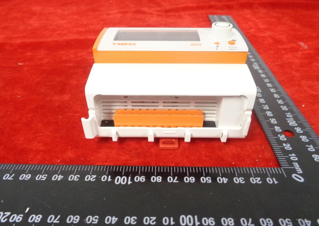
Click to zoom
Application Details
- Equipment Class
- DTS - Digital Transmission System
- Date of Grant
- Jan 11, 2023
- Application Purpose
- Original Equipment
- Date of Application
- Jan 02, 2023
- Equipment Note
- IQ5-IO-8DO-HOA-B, IQ5-IO-8DO-B
- Frequency Range
- 2402.00000000 - 2480.00000000
- Company
- Honeywell International Inc
- Country
- United States
Documents & Files
Document Text
Text extracted from the exhibit documents filed with the FCC. Open a document above to read the original.
Users Manual
D Data Sheet IQ5 I/O Module Description The IQ®5-IO range of I/O modules are designed for use with the IQ5 controller, to provide input and output channel connection points. A comprehensive choice of I/O types is available including universal inputs/outputs (UIO), digital inputs (DI), digital/relay outputs (DO). A ‘hand-off -auto’ variant (8DO-HOA) is also available, off ering manual override of module outputs. Integral I/O bus connectors allow easy and convenient ‘side- byside’ module installation or, by using wiring adapters, modules can be installed up to 300 meters apart. Features ▪ Universal input/output, digital input, digital output variants ▪ Hand-off -auto option (on 8DO-HOA) ▪ Up to 300 I/O channels per controller (subject to licence) ▪ T1L high-speed secure bus connection to controller ▪ Side-by-side or remote connection options ▪ Up to 300 metres (1000 ft) between cable connected modules ▪ Powered from controller or external PSU ▪ Two part I/O connectors for easy installation/commissioning ▪ Surface or DIN rail mounting, DIN 19 size 2 standard enclosur ▪ IQ5-IO I/O Module D Physical FUNCTIONALITY HARDWARE The range of IQ5-IO Expansion Modules comprises the following variants: 16UIO 16DI 8DO 8DO-HOA 8UIO-105 Note: All modules shown with terminal covers removed. 3 Enclosure Each IQ5-IO Module is housed in a polycarbonate enclosure compatible with the DIN43880 and DIN 19 size 2 standard and with a complimentary styling to the IQ5 controller. Integral clips on the back of the case enable the unit to be clipped on to (and quickly released from) a standard TS35 DIN rail, or be used to mount the unit directly to any suitable flat surface. IQ5-IO Modules must be installed in a secondary enclosure with a minimum protective rating of IP20 (or equivalent) or mounted outside normal reach (e.g. in a plenum). A module may be mounted horizontally or vertically but not upside down or on its back: Removable clip-on polycarbonate covers provide access to the various onboard terminal connections. Spare covers are available (see ‘Order Codes’ on page 13) Terminal Connectors Connections for the various I/O channels are via two-part plugable screw terminal connectors which are supplied as standard with the modules and available in packs for spares. Optional connectors with push-fit terminals are also available (see ‘Order Codes’ on page 13). Function Connector Type Universal Input/Output (UIO) 2-way* Digital Input (DI) 2-way Digital/Relay Output (DO) 3-way *On the 16UIO, input IO8 uses a 3-way connector with the extra terminal providing a connection to the 24 Vdc supply output. Auxiliary Terminal Block Optional terminal blocks are available that can be clipped on to an IO module to provide additional common terminals. These can be used (for example) to provide multiple 24 Vdc connections from the single 24 Vdc terminal on the 16UIO or 8UIO module, or to provide ground/earth connections for cable screens. The AUX-TRM-16 has 16 push-fit terminals, configured as two common groups of 8 with a maximum load of 12 A. If more terminals are needed the connectors can be ‘doublestacked’. Input/Output Channels The following types of input and output channel are supported: ▪ Universal Input/Output (UIO) ▪ Digital Inputs (DI) ▪ Digital/Relay Output (DO) Cable Screening The use of screened cable for input and/or output connections is optional and not generally required unless the cable passes through electrically noisy environments. If screened cable is used the screen must be connected to the local panel/enclosure ground and left unterminated at the far end. Universal Input/Output (UIO) These channels will function in one of the following modes: ▪ thermistor input, ▪ voltage input, ▪ digital input, ▪ current input, ▪ analogue output. The input/output mode of each channel is set by the strategy configuration in the controller. Thermistor input: Used for a thermistor (e.g. NTC (2K, 3K, 10K, 20K), PT100, PT1000) potentiometer (0 to 300 kΩ) or fan speed control. The thermistor bridge resistor is 12 kΩ with a bridge supply 3.3 V. Example wiring Voltage input: Used with a 0 to 10 Vdc or 2 to 10 Vdc source. C nn IO n nn Data Sheet 4 Example wiring Digital input: Used for a volt free contact, logic circuit (e.g. TTL, CMOS), open collector (transistor) or open drain (FET). Example wiring free collector circuit The volt free contact has a nominal wetting current of 3.5 mA. The input is ON when the contact is closed. An open collector or open drain must be able to sink 3.5 mA. The input is ON when the transistor or FET conducts. A logic circuit must be able to sink 3.5 mA. The input will be ON when the applied voltage is less than 2 Vdc (minimum 0 V). A voltage of greater than 4 Vdc (maximum 40 Vdc) will turn the input OFF. Voltage levels between 2 and 4 Vdc may cause indeterminate operation. The input can be configured for pulse count operation (maximum 100 Hz with 50% / 50% duty cycle, 5 ms ON /5 ms OFF). Current input: Used for 0 or 4 to 20 mA sources. May be either loop powered (from onboard 24VDC OUT terminal) or externally powered. Example wiring - loop Example wiring - external External Power Supply Note: The 24VDC OUT terminal can source up to 75 mA. Analogue output: Provides either a variable voltage output (0 to 11 Vdc, 0 to 10 Vdc, 1 to 10 Vdc or 2 to 10 Vdc) or variable current output (0 to 20 mA or 4 to 20 mA). Example wiring Digital Input (DI) These channels are compatible with the following input devices: ▪ volt free contact (e.g. switch or relay), ▪ logic circuit (e.g. TTL, CMOS), ▪ open collector (transistor) or open drain (FET),or ▪ 24 Vac circuit. Example wiring free collector circuit The volt free contact has a nominal wetting current of 3.5 mA. The input is ON when the contact is closed. An open collector or open drain must be able to sink 3.5 mA. The input is ON when the transistor or FET conducts. A logic circuit must be able to sink 3.5 mA. The input will be ON when the applied voltage is less than…
Text truncated - open the document above for the full version.
Cover Letter(s)
TCB Authority to Act as Agent Number: MS-0045317 Revision: 0 Effective date: Oct 8, 2021 Page 1 of 1 Honeywell International Inc. Authority to Act as Agent Date: 2022-11-25 TUV Rheinland of North America, Inc. 1279 Quarry Lane., Suite. A Pleasanton, CA 94566 To Whom It May Concern: I appoint TÜV Rheinland (China) Ltd. & Mr. Zhu Qiusheng to act as our agent in the preparation of this application for equipment certification. I certify that submitted documents properly describe the device or system for which equipment certification is sought. I also certify that each unit manufactured, imported or marketed, as defined in the FCC or Industry Canada’s regulations will have affixed to it a label identical to that submitted for approval with this application. For instances where our authorized agent signs the application for certification on our behalf, I acknowledge that all responsibility for complying with the terms and conditions for Certification, as specified by TUV Rheinland Group, still resides with Honeywell International Inc. 12 Clintonville Road, Northford, CT 06472, United States. For TCB applications, We certify that we are not subject to denial of federal benefits, that includes FCC benefits, pursuant to Section 5301 of the Anti-Drug Abuse Act of 1988, 21 U.S.C. 862. Further, no party, as defined in 47 CFR 1.2002 (b), to the application is subject to denial of federal benefits, that includes FCC benefits. Thank you, Agency Agreement Date: ___2022-11-25________________ Agreement is valid for 12 months from the above date. By: __________________________ ___ Luke Sisson _ ( Signature) (Print name) _ Advanced Certification Engineer (203)484-6154 (Title) (Telephone) On behalf of: Honeywell International Inc (Company Name)
Cover Letter(s)
Family Certification information To whom it may concern, W e, Honeywell International Inc. hereby confirm that the family models are listed in the following table. No . HVIN PMN Remarks 01 601001 IQ5- IO- 8DO- B The electrical circuit design and PCB layout are identical, only the materials of the display are different for market strategy. 02 601001 IQ5- IO- 8DO- HOA- B T hese models are identical as follows: Electronics/electrical designs, including software & firmware Construction Design/Physical Design PCB Layout (Others, please specify): The only differences between these models are the follows for marketing purpose: Product name The screen portions ( LED screen used for IQ5- IO- 8DO- B, LCD screen sued for IQ5- IO- 8DO- HOA- B ), which has no affections on the RF characteristics. R egards, S ignature: P rint Name / Title: Luke Sisson / Advanced Certification Engineer D ate: 2022.11.29
External Photos
IQ5-IO-8DO-B IQ5-IO-8DO-HOA-B
Internal Photos
IQ5-IO-8DO-B IQ5-IO-8DO-HOA-B
Operational Description
1 EMVANGO T1L_8DO_HOA BLE Antenna Test Report 2022/03/23 电磁方圆www.emvango.com BLE Antenna Type:PCBAntenna www.emvango.com 2 BLE Antenna Frequency Range:2400MHz-2480MHz BLE Antenna Peak Gain:3.1dBi Frequency (MHz)24002405241024152420242524302435244024452450245524602465247024752480 Efficiency (%) 55.898757.752759.582758.018956.625858.366658.76156.675757.752757.763858.636961.047859.158359.798458.548957.41357.165 Gain (dBi) 2.563042.688643.070632.581372.971263.107282.670642.725272.88743.097183.068452.989773.106532.739343.037352.796512.83558 BLE Antenna Pattern www.emvango.com 3 XY-PlaneYZ-PlaneXZ-Plane Thank you! 电磁方圆www.emvango.com 4
RF Exposure Info
Prüfbericht - Produkte Test Report - Products Page 1 of 3 RF Exposure Compliance RESULT: Pass Test standard : RSS-102 Issue 5 FCC Part 1.1091 Limit : Table 1 of 47 CFR FCC Part 1.1310 Section 2.5.2 of RSS-102 Issue 5 Kind of test site : Shielded room This device is mobile device, and the applicant declares that the minimum separation distance is greater than 20cm. Therefore MPE measurement or computational modelling should be used to determine compliance. MPE Calculation is based on the conducted power, and considering maximum power and Antenna gain. The following formula is used to MPE evaluation. 2 4 * R GPout Pd Where P d = power density in mW/cm 2 or W/m 2 P out = output power to antenna in mW or W G num = Antenna gain in numeric π = 3.14159 R = Distance between observation point and the center of radiator in cm or m Prüfbericht - Produkte Test Report - Products Page 1 of 3 FCC Part 1.1310, Part 2.1091 MPE-Based Evaluation: Inclusion: The MPE is much lower than the limit. Operating Mode Max. EIRP incl. tune-up (dBm) Distance (cm) MPE (mW/cm2) Limit (mW/cm2) Verdict BLE 8.5 20 0.0029 1.0 Pass The Max antenna gain is 3.1dBi. Prüfbericht - Produkte Test Report - Products Page 1 of 3 RSS-102 Exemption Limits for Routine Evaluation – RF Exposure Evaluation RF exposure evaluation is required if the separation distance between the user and/or bystander and the device’s radiating element is greater than 20 cm, except when the device operates as follows: • below 20 MHz and the source-based, time-averaged maximum e.i.r.p. of the device is equal to or less than 1 W (adjusted for tune-up tolerance); • at or above 20 MHz and below 48 MHz and the source-based, time-averaged maximum e.i.r.p. of the device is equal to or less than 4.49/ƒ0.5 W (adjusted for tune-up tolerance), where ƒ is in MHz; • at or above 48 MHz and below 300 MHz and the source-based, time-averaged maximum e.i.r.p. of the device is equal to or less than 0.6 W (adjusted for tune-up tolerance); • at or above 300 MHz and below 6 GHz and the source-based, time-averaged maximum e.i.r.p. of the device is equal to or less than 1.31 x 10⁻² ƒ0.6834 W (adjusted for tune-up tolerance), where ƒ is in MHz; • at or above 6 GHz and the source-based, time-averaged maximum e.i.r.p. of the device is equal to or less than 5 W (adjusted for tune-up tolerance). In these cases, the information contained in the RF exposure technical brief may be limited to information that demonstrates how the e.i.r.p. was derived. RF Exposure Calculations for ISED Operating Mode Max. EIRP incl. tune-up (dBm) Distance (cm) Maximu m EIRP (W) Thresho ld power (W) Verdict BLE 8.5 20 0.0145 2.68 Pass Note: The maximum EIRP much lower than the threshold power in section 2.5.2, thus compliant. The Max antenna gain is 3.1Bi.
Test Report
Prüfbericht - Produkte Test Report - Products Prüfbericht-Nr.: Test report no.: CN22OBY1 001 Auftrags-Nr.: Order no.: 168376481 Seite 1 von 20 Page 1 of 20 Kunden-Referenz-Nr.: Client reference no.: N/A Auftragsdatum: Order date: 2022-06-09 Auftraggeber: Client: Honeywell International Inc. 12 Clintonville Road, Northford, CT 06472, United States Prüfgegenstand: Test item: I/O Module Bezeichnung / Typ-Nr.: Identification / Type no.: IQ5-IO-8DO-B, IQ5-IO-8DO-HOA-B Auftrags-Inhalt: Order content: Test Report Prüfgrundlage: Test specification: CFR47 FCC Part 15: Subpart C Section 15.247 RSS-247 Issue 2 February 2017 RSS-Gen Issue 5 March 2019 Wareneingangsdatum: Date of sample receipt: 2022-06-09 Please refer to Photo Document Prüfmuster-Nr.: Test sample no: A003268712-005, 014 A003274086-019,023 Prüfzeitraum: Testing period: 2022-06-13 – 2022-07-13 Ort der Prüfung: Place of testing: TÜV Rheinland (Shenzhen) Co., Ltd. Prüflaboratorium: Testing laboratory: TÜV Rheinland (Shenzhen) Co., Ltd. Prüfergebnis*: Test result*: Pass geprüft von: tested by: X Signed by: Bell Hu genehmigt von: authorized by: X Signed by: Lin Lin Datum: Date: 2022-07-20 Ausstellungsdatum: Issue date: 2022-07-20 Stellung / Position: Project Manager Stellung / Position: Reviewer Sonstiges / Other: FCC ID: 2A8LT-IQ5IO8DOB IC: 1609A-IQ5IO8DOB, PMN: IQ5-IO-8DO-B, IQ5-IO-8DO-HOA-B HVIN: 601001 Zustand des Prüfgegenstandes bei Anlieferung: Condition of the test item at delivery: Prüfmuster vollständig und unbeschädigt Test item complete and undamaged * Legende: 1 = sehr gut 2 = gut 3 = befriedigend 4 = ausreichend 5 = mangelhaft P(ass) = entspricht o.g. Prüfgrundlage(n) F(ail) = entspricht nicht o.g. Prüfgrundlage(n) N/A = nicht anwendbar N/T = nicht getestet * Legend: 1 = very good 2 = good 3 = satisfactory 4 = sufficient 5 = poor P(ass) = passed a.m. test specification(s) F(ail) = failed a.m. test specification(s) N/A = not applicable N/T = not tested Dieser Prüfbericht bezieht sich nur auf das o.g. Prüfmuster und darf ohne Genehmigung der Prüfstelle nicht auszugsweise vervielfältigt werden. Dieser Bericht berechtigt nicht zur Verwendung eines Prüfzeichens. This test report only relates to the a. m. test sample. Without permission of the test center this test report is not permitted to be duplicated in extracts. This test report does not entitle to carry any test mark. TÜV Rheinland (Shenzhen) Co., Ltd. 1601 R&D Room, 1602-1604, 17-18F, Building 7 Site C, Vanke Cloud City Phase I, Xingke First Street, Xili Street, Xili Community, Nanshan District, Shenzhen 518052, P.R. China Mail: [email protected] · Web: www.tuv.com Prüfbericht - Produkte Test Report - Products Prüfbericht - Nr.: Test Report No.: CN22OBY1 001 Seite 2 von 20 Page 2 of 20 Test Summary 5.1.1 ANTENNA REQUIREMENT RESULT: Pass 5.1.2 MAXIMUM PEAK CONDUCTED OUTPUT POWER RESULT: Pass 5.1.3 CONDUCTED POWER SPECTRAL DENSITY RESULT: Pass 5.1.4 6DB BANDWIDTH RESULT: Pass 5.1.5 99% BANDWIDTH RESULT: Pass 5.1.6 CONDUCTED SPURIOUS EMISSIONS MEASURED IN 100 KHZ BANDWIDTH RESULT: Pass 5.1.7 RADIATED SPURIOUS EMISSION RESULT: Pass 5.1.8 CONDUCTED EMISSION ON AC MAINS RESULT: Pass Prüfbericht - Produkte Test Report - Products Prüfbericht - Nr.: Test Report No.: CN22OBY1 001 Seite 3 von 20 Page 3 of 20 Contents 1 GENERAL REMARKS ........................................................................................................................... 4 1.1 COMPLEMENTARY MATERIALS ............................................................................................................ 4 2 TEST SITES ........................................................................................................................................ 5 2.1 TEST FACILITIES ................................................................................................................................. 5 2.2 LIST OF TEST AND MEASUREMENT INSTRUMENTS................................................................................. 5 2.3 TRACEABILITY .................................................................................................................................... 6 2.4 CALIBRATION ..................................................................................................................................... 6 2.5 MEASUREMENT UNCERTAINTY............................................................................................................. 6 2.6 LOCATION OF ORIGINAL DATA ............................................................................................................. 6 2.7 STATUS OF FACILITY USED FOR TESTING ............................................................................................. 6 3 GENERAL PRODUCT INFORMATION ...................................................................................................... 7 3.1 PRODUCT FUNCTION AND INTENDED USE ............................................................................................. 7 3.2 RATINGS AND SYSTEM DETAILS .......................................................................................................... 7 3.3 INDEPENDENT OPERATION MODES ...................................................................................................... 8 3.4 NOISE GENERATING AND NOISE SUPPRESSING PARTS ......................................................................... 8 3.5 SUBMITTED DOCUMENTS..................................................................................................................... 8 4 TEST SET-UP AND OPERATION MODES ................................................................................................ 9 4.1 PRINCIPLE OF CONFIGURATION SELECTION ......................................................................................... 9 4.2 TEST OPERATION AND TEST SOFTWARE .............................................................................................. 9 4.3 SPECIAL ACCESSORIES AND AUXILIARY EQUIPMENT ....................…
Text truncated - open the document above for the full version.
Test Setup Photos
Prüfbericht - Produkte Test Report - Products Appendix A CN22OBY1 001 Page 1 of 3 Appendix A: Photographs of the Test Set-Up APPENDIX A: PHOTOGRAPHS OF THE TEST SET-UP ....................................................................................................... 1 PHOTOGRAPH 1: SET-UP PHOTO FOR RADIATED SPURIOUS EMISSION, 30MHZ - 1GHZ ...................................................................... 2 PHOTOGRAPH 2: SET-UP PHOTO FOR RADIATED SPURIOUS EMISSION, 1GHZ - 18GHZ....................................................................... 2 PHOTOGRAPH 3: SET-UP PHOTO FOR CONDUCTED EMISSION ON AC MAINS ..................................................................................... 3 Prüfbericht - Produkte Test Report - Products Appendix A CN22OBY1 001 Page 2 of 3 Photograph 1: Set-up photo for Radiated Spurious Emission, 30MHz - 1GHz Photograph 2: Set-up photo for Radiated Spurious Emission, 1GHz - 18GHz Prüfbericht - Produkte Test Report - Products Appendix A CN22OBY1 001 Page 3 of 3 Photograph 3: Set-up photo for Conducted Emission on AC Mains
Contact Information
Applicant
Luke Sisson(Advanced Certification Engineer)
Technical Contact
Test Firm
TUV Rheinland (Shenzhen) Co., Ltd.Gina Yang
[email protected]86 755 8268 1497
Technical Specifications
| # | Rule Parts | Frequency Range | Power Output |
|---|---|---|---|
| 1 | 15C | 2.40 GHz - 2.48 GHz | 7.10 mW |
Other Applications from Honeywell International Inc
2A8LT-E28POINT
Jan 08, 2026I/O Module
Equipment Class
DTS - Digital Transmission System2A8LT-24DX47
Jun 25, 2024INNCOM DX47 Controller-X47
Equipment Class
DTS - Digital Transmission System2A8LT-ADVBLEWIFI
May 05, 2024Plant controller
Equipment Class
DTS - Digital Transmission System2A8LT-IQ5IODI
Jan 21, 2024I/O Module
Equipment Class
DTS - Digital Transmission System2A8LT-IQ5IOB
Jan 21, 2024I/O Module
Equipment Class
DTS - Digital Transmission System