2A8PN-EC254G module
Sunivision Technology Development Company Limited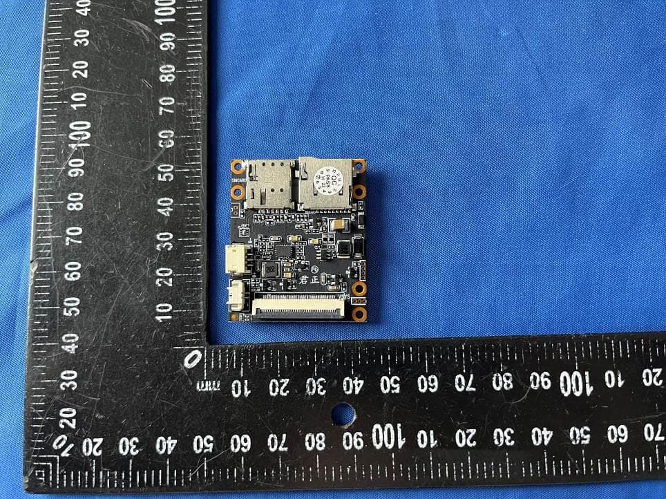
Click to zoom
Application Details
- Equipment Class
- PCB - PCS Licensed Transmitter
- Date of Grant
- Sep 26, 2022
- Application Purpose
- Original Equipment
- Date of Application
- Sep 26, 2022
- Equipment Note
- 4G module
- Frequency Range
- 699.00000000 - 716.00000000
- Country
- China
Documents & Files
Document Text
Text extracted from the exhibit documents filed with the FCC. Open a document above to read the original.
Users Manual
RF LAYOUT Application Guide Sunivision Technology Development Co.,Ltd 1 / 9 RF LAYOUT Application Guide Version: RF LAYOUT_Application Guide_V2.2 Date: 2016-02-26 Document History ................................................ ...................................................... ...................................................... .................2 Table of Contents ................................ ...................................................... ...................................................... ................................. 3 Picture Index... ...................................................... ...................................................... ...................................................... .............4 1 3 50 Ohm characteristic impedance coplanar waveguide structure design................................................ ...................................................... ............................... 7 4 Coplanar Waveguide PCB LAYOUT Examples and Precautions ................................ ...................................................... .............9 2 RF Interface Schematic Recommendations................................................ ...................................................... .................................6 RF LAYOUT Application Guide 2 / 9 introduction................................................. ...................................................... ...................................................... .................5 Sunivision Technology Development Co.,Ltd Table of contents Sunivision Technology Development Co.,Ltd 3 / 9 RF LAYOUT Application Guide image index Figure 2: Schematic diagram of coplanar waveguide structure ................................................ ...................................................... ............................................... 7 Figure 4: Schematic diagram of four-layer board LAYOUT (the reference ground is the third layer)................................. ...................................................... ......... 8 Figure 6: Example diagram of PCB LAYOUT................................................ ...................................................... ......................................... 9 Figure 5: Schematic diagram of four-layer board LAYOUT (the reference ground is the fourth layer)................................. ...................................................... ......... 8 Figure 3: Schematic diagram of two-layer board LAYOUT................................................ ...................................................... ....................................... 8 Figure 1: Module RF Reference Schematic ............................................... ...................................................... ............................................... 6 RF part PCB layout design to ensure RF LTE modules. 4 / 9 Sunivision Technology Development Co.,Ltd performance, reducing customer design cycles. This document applies to all Quectels This document mainly introduces the PCB routing precautions of the module's peripheral RF circuit to help customers to correctly carry out when using the Quectel module. RF LAYOUT Application Guide 1 Introduction Support Bands : LTE Band 2/4/5/12 Among them, C1, R1, and C2 are reserved matching circuits to optimize the performance of the antenna port. The default values are: R1 is pasted with 0R resistor; C1 is not pasted; C2 is not pasted. 5 / 9 Sunivision Technology Development Co.,Ltd Figure 1: Module RF Reference Schematic RF LAYOUT Application Guide 2 RF Interface Schematic Recommendations 0.076mm Figure 2: Schematic diagram of the coplanar waveguide structure 0.1623mm Sunivision Technology Development Co.,Ltd 6 / 9 The main factors affecting the characteristic impedance of coplanar waveguides are the dielectric constant of the substrate (usually 0.1188mm Line width W It is recommended to use the coplanar waveguide microwave transmission form, and the characteristic impedance is 50 ohms, as shown in Figure 2. Ground clearance S 0.24mm 0.2mm 0.2mm Table 1: 50 ohm coplanar waveguide line width and recommended distance to ground corresponding to the distance between different signal layers and reference ground RF LAYOUT Application Guide Distance H between signal layer and reference ground 0.15mm 4.2ÿ4.6, take here 4.4), the distance between the signal layer and the reference ground H, the line width W, the ground clearance S, and the copper thickness T. Table 1 lists the distance H between different signal layers and the reference ground 0.15mm 0.1mm When the thickness of copper skin is T=0.035mm, the line width W corresponding to the characteristic impedance of 50 ohms and the recommended value of the ground clearance S: 3 50 Ohm Characteristic Impedance Coplanar Waveguide Structure Design 0.15mm 0.18mm If it is a 2-layer board, the signal layer is the Top layer, and the reference ground is the Bottom layer, as shown in Figure 3 below. If it is a 4-layer board, the reference ground can be the 2nd Figure 4: Schematic diagram of the four-layer board LAYOUT (the reference ground is the third layer) Figure 5: Schematic diagram of the four-layer board LAYOUT (the reference ground is the fourth layer) 1.0mm 2mm Sunivision Technology Development Co.,Ltd 0.8mm 7 / 9 1.6mm 0.8mm 0.8mm It is 5 times the width of the signal line, as shown in Figure 5 below. If it is more than 6-layer board and so on. Figure 3: Schematic diagram of two-layer board LAYOUT Layer, Layer 3 or Layer 4. If the reference ground is the third layer, the second layer directly under the signal layer should be forbidden, and the width of the forbidden area should be at least the signal line. 0.8mm RF LAYOUT Application Guide 0.16mm 0.8mm 0.17mm 0.8mm 5 times the width, as shown in Figure 4 below. If the reference ground is the 4th layer, the 2nd and 3rd layers directly under the signal layer must be forbidden to be laid, and the width of …
Text truncated - open the document above for the full version.
Cover Letter(s)
Sunivision Technology Development Company Limited Office of Engineering Technology Federal Communications Commission 7435 Oakland Mills Road Columbia, MD 21046 Date: September 17, 2022 Subject; Request for Long Term Confidentiality FCC ID: 2A8PN-EC25 To Whom It May Concern, Pursuant to the provisions of the Commission’s rules Title 47 Sections §0.457 and §0.459, we are requesting the Commission to withhold the following attachment(s) as confidential documents from public disclosure indefinitely. These documents contain detailed system and equipment descriptions and are considered as proprietary information in operation of the equipment. The public disclosure of these documents might be harmful to our company and would give competitors an unfair advantage in the market. Schematic Diagram Block Diagram Operational Description BOM Tune up It is our understanding that all measurement test reports, FCC ID label format and correspondence during the certification review process cannot be granted as confidential documents and this information will be available for public review once the grant of equipment authorization is issued. Sincerely, Signature: September 17, 2022 Name Nick Xiong Position Sales Manager Company Name Sunivision Technology Development Company Limited Address Floor 3, Building B, TaoYuan Industrial Park, Huangpu East Development Zone, Guangzhou, China Tel +86-20-32071803 Fax +86-20-32071803 Email [email protected]
Cover Letter(s)
Sunivision Technology Development Company Limited September 17, 2022 Nemko Canada Inc 303 River Road Ottawa, Ontario, Canada K1V 1H2 Attn: Director of Certification Authority to Act as Agent On our behalf, I appoint Shenzhen Alpha Product Testing Co., Ltd. Address: Building i, No.2, Lixin Road, Fuyong Street, Bao’an District, 518103, Shenzhen, Guangdong, China Person: Mark Zhu (Name and address,person). To act as our agent in the preparation of this application for equipment certification. I certify that submitted documents properly describe the device or system for which equipment certification is sought. I also certify that each unit manufactured, imported or marketed, as defined in the Federal Communications Commission’s regulations will have affixed to it a label identical to that submitted for approval with this application. For instances where our authorized agent signs the application for certification on our behalf, I acknowledge that all responsibility for complying with the terms and conditions for certification, as specified by Nemko Canada Inc, still resides with Sunivision Technology Development Company Limited. Address: Floor 3, Building B, TaoYuan Industrial Park, Huangpu East Development Zone, Guangzhou, China (applicant name and address). Signature: September 17, 2022 Name Nick Xiong Position Sales Manager Company Name Sunivision Technology Development Company Limited Address Floor 3, Building B, TaoYuan Industrial Park, Huangpu East Development Zone, Guangzhou, China Tel +86-20-32071803 Fax +86-20-32071803 Email [email protected]
Cover Letter(s)
FCC Modular Approval Request To the FCC or FCC TCB handling this application Hereby we, Company (grantee) Sunivision Technology Development Company Limited Addresss Floor 3, Building B, TaoYuan Industrial Park, Huangpu East Development Zone, Guangzhou, China City / ZIP / State / Country China request modular approval for the certification of our equipment within this application, identified by: FCC ID: 2A8PN-EC25 The table below contains justification for modular approval of this equipment. Requirement per DA 00-1407 Explanation from grantee 1. The modular transmitter must have its own RF shielding. Has RF shielding. 2.The modular transmitter must have buffered modulation/data inputs (if such inputs are provided) to ensure that the module will comply with Part 15 requirements under conditions of excessive data rates or over-modulation. The modular have buffered modulation/data inputs. 3. The modular transmitter must have its own power supply regulation. The modular transmitter have its own power supply regulation. 4.The modular transmitter must comply with the antenna requirements of Section 15.203 and 15.204(c). The antenna must either be permanently attached or employ a “unique” antenna coupler (at all connections between the module and the antenna, including the cable).. This module is equipped with a PCB antenna, please refer to the External Photo for the detail. 5. The modular transmitter must be tested in a stand-alone configuration, i.e., the module must not be inside another device during testing. This is intended to demonstrate that the module is capable of complying with Part 15 emission limits regardless of the device into which it is eventually installed. The module was tested in a stand-alone configuration, please refer to the Setup Photo for the detail 6. The modular transmitter must be labeled with its own FCC ID number, and, if the FCC ID is not visible when the module is installed inside another device, then the outside of the device into which the module is installed must also display a label referring to the enclosed module. This exterior label can use wording such as the following: “Contains Transmitter Module FCC ID: ??????????” or “Contains FCC ID: 2A8PN-EC25” Any similar wording that expresses the same meaning may be used. The Grantee may either provide such a label, an example of which must be included in the application for equipment authorization, or, must provide adequate instructions along with the module which explain this requirement. In the latter case, a copy of these instructions must be included in the application for equipment authorization. Please refer to label sample exhibit - host labeling is described in integration manual 7. The modular transmitter must comply with any specific rule or operating requirements applicable to the transmitter and the manufacturer must provide adequate instructions along with the module to explain any such requirements. A copy of these instructions must be included in the application for equipment authorization. For example, there are very strict operational and timing requirements that must be met before a transmitter is authorized for operation under Section 15.231. For instance, data transmission is prohibited, except for operation under Section 15.231(e), in which case there are separate field strength level and timing requirements. Compliance with these requirements must be assured. The required FCC rule has been fulfilled and all the instructions for the maintaining compliance have been clearly stated in the User Manual. 8. The modular transmitter must comply with any applicable RF exposure requirements. For example, FCC Rules in Sections 2.1091, 2.1093 and specific Sections of Part 15, including 15.319(i), 15.407(f), 15.253(f) and 15.255(g), require that Unlicensed PCS, UNII and millimetre wave devices perform routine environmental evaluation for RF Exposure to demonstrate compliance. In addition, spread spectrum transmitters operating under Section 15.247 are required to address RF Exposure compliance in accordance with Section 15.247(b)(4). Modular transmitters approved under other Sections of Part 15, when necessary, may also need to address certain RF Exposure concerns, typically by providing specific installation and operating instructions for users, installers and other interested parties to ensure compliance. The MPE evaluation with 20cm distance restriction is submitted for the compliance of RF Exposure requirement. Attestation (by grantee) City and Country: Date: Name: (this must be a person) Function: Signature: (or official company stamp) Guangzhou, China 2022.09.17 Nick Xiong Sales Manager
External Photos
FCC ID: 2A8PN-EC25 ANT
ID Label/Location Info
Label Location FCC ID: 2A8PN-EC25
Internal Photos
FCC ID: 2A8PN-EC25
RF Exposure Info
FCC ID: 2A8PN-EC25 Prediction of MPE at a given distance 1. Limits The criteria listed in the following table shall be used to evaluate the environment impact of human exposure to radio frequency (RF) radiation as specified in 1.1307(b) 2. Test Procedure Equation from page 18 of OET Bulletin 65, Edition 97-01 Where: S = power density P = power input to the antenna G = numeric gain of the antenna in the direction of interest relative to an isotropic radiator R = distance to the centre of radiation of the antenna FCC ID: 2A8PN-EC25 3. Result Mode Frequency (MHz) Prediction distance (cm) Rated Peak RF power output MPE (mW/cm 2 ) Limit (mW/cm 2 ) SAR Test Exclusion dBm mW LTE B2 1850-1910 20 24 251.189 0.079 1 Yes LTE B4 1710-1755 20 24 251.189 0.079 1 Yes LTE B5 824-849 20 24 251.189 0.079 0.549 Yes LTE B12 699-716 20 24 251.189 0.079 0.466 Yes LTE Antenna Gain: 1.97dBi, 1.57(numeric) Then SAR evaluation is not required.
Test Report
ALPHA's reports is using a digital certificate that is trusted on Adobe's official server. If there is no digital certificate or the digital certificate shows damaged in your report. Please do not accept the report. FCC TEST REPORT FCC ID: 2A8PN-EC25 On Behalf of Sunivision Technology Development Company Limited 4G module Model No.: Quectel EC25 Prepared for : Sunivision Technology Development Company Limited Address : Floor 3, Building B, TaoYuan Industrial Park, Huangpu East Development Zone, Guangzhou, China Prepared By : Shenzhen Alpha Product Testing Co., Ltd. Address : Building i, No.2, Lixin Road, Fuyong Street, Bao'an District, 518103, Shenzhen, Guangdong, China Report Number : A2206125-C01-R01 Date of Receipt : August 10, 2022 Date of Test : September 1, 2022- September 13, 2022 Date of Report : September 13, 2022 Version Number : V0 Page 2 of 153 Report No.: A2206125-C01-R01 TABLE OF CONTENTS Description Page 1 TEST SUMMARY ......................................................................................................................................5 2 GENERAL INFORMATION .......................................................................................................................6 2.1 GENERAL DESCRIPTION OF EUT ..........................................................................................................6 2.2 RELATED SUBMITTAL(S) / GRANT (S) ....................................................................................................7 2.3 TEST FACILITY.....................................................................................................................................7 2.4 ACCESSORIES OF DEVICE (EUT) .........................................................................................................7 2.5 TESTED SUPPORTING SYSTEM DETAILS ...............................................................................................7 2.6 TEST CONDITIONS ...............................................................................................................................7 2.7 MEASUREMENT UNCERTAINTY .............................................................................................................8 3 TEST INSTRUMENTS LIST ......................................................................................................................9 4 SYSTEM TEST CONFIGURATION ........................................................................................................10 4.1 TEST MODE .......................................................................................................................................10 4.2 CONFIGURATION OF TESTED SYSTEM .................................................................................................10 4.3 CONDUCTED OUTPUT POWER ............................................................................................................11 4.4 PEAK-TO-AVERAGE RATIO .................................................................................................................22 4.5 OCCUPY BANDWIDTH .........................................................................................................................26 4.6 MODULATION CHARACTERISTIC ................................................................................................39 4.7 OUT OF BAND EMISSION AT ANTENNA TERMINALS ................................................................................39 4.8 ERP, EIRP MEASUREMENT ...............................................................................................................90 4.9 FIELD STRENGTH OF SPURIOUS RADIATION MEASUREMENT ................................................................132 4.10 FREQUENCY STABILITY V.S. TEMPERATURE MEASUREMENT ..............................................................142 4.11 FREQUENCY STABILITY V.S. VOLTAGE MEASUREMENT ......................................................................145 4.12 TEST SETUP PHOTO ........................................................................................................................147 Page 3 of 153 Report No.: A2206125-C01-R01 TEST REPORT DECLARATION Applicant : Sunivision Technology Development Company Limited Address : Floor 3, Building B, TaoYuan Industrial Park, Huangpu East Development Zone, Guangzhou, China Manufacturer : Sunivision Technology Development Company Limited Address : Floor 3, Building B, TaoYuan Industrial Park, Huangpu East Development Zone, Guangzhou, China EUT Description : 4G module (A) Model No. : Quectel EC25 (B) Trademark : N/A Measurement Standard Used: FCC CFR Title 47 Part 2 FCC CFR Title 47 Part 22 Subpart H FCC CFR Title 47 Part 24 Subpart E FCC CFR Title 47 Part 27 ANSI C63.26:2015 The device described above is tested by Shenzhen Alpha Product Testing Co., Ltd. to determine the maximum emission levels emanating from the device. The test results are contained in this test report and Shenzhen Alpha Product Testing Co., Ltd. is assumed of full responsibility for the accuracy and completeness of these tests. After the test, our opinion is that EUT compliance with the requirement of the above standards. This report applies to above tested sample only. This report shall not be reproduced in parts without written approval of Shenzhen Alpha Product Testing Co., Ltd. Tested by (name + signature).........: Lucas Pang Project Engineer Approved by (name + signature).......: Jack Xu Project Manager Date of issue.............................: September 13, 2022 Page 4 of 153 Report No.: A2206125-C01-R01 Revision History Revision Issue Date Revisions Revised By V0 September 13, 2022 Initial released Issue Lucas Pang Page 5 of 153 Report No.: A2206125-C01-R01 1 Test Summary Test Item Section in CFR 47 Result RF Exposure (SAR) Part 1.1307 Part 2.1093 Pass*(Please refer to SAR Report) RF Output Power Part 2.1046 Part 22.913(a) (5) Part 24.232 (c) Part 27.50 (d)(4) Part 27.50 (h) Pass Peak-To-Average Ratio Part 2.104…
Text truncated - open the document above for the full version.
Test Report
QR/RD-P01-06B SPECIFICATION ShenzhenGuandetongElectronicLimited 深圳市冠得通电子有限公司 ShenzhenGuandetongElectronicCo.,Ltd. 4G5dBi刀锋胶棒天线 产品规格书 客户频段824-960/1710-2690MHZ 线材名称版本A1 客户料号冠得通料号 冠得通编号 RF设计肖彬射频经理刘亮 结构设计王栋结构经理王华 技术总监 ANDY 日期 2020-06-15 客户确认: 装配是否符合贵司要求:□ OK □ NG 深圳市冠得通电子有限公司 保密要求 本公司已拥有专有技术所提供的资料,这些专有资料应严加保密,在未经深圳冠得通电子有限公司事先书面同意的时不允许 透露给任何人或公司。 公司地址:深圳市龙华区观湖街道环观南茂源工业园D栋3楼电话:0755-88298396传真:0755-89733896 http://www.szgdtrf.com Page2 目录 封面.......................................................................................................1 目录..........................................................................................2 一、产品图片......................................................................................3 二、产品参数.......................................................................................3 三、S11数据.................................................................................4 四、产品结构图...................................................................................5 五、环境可靠性实验报告..................................................................6 深圳市冠得通电子有限公司 保密要求 本公司已拥有专有技术所提供的资料,这些专有资料应严加保密,在未经深圳冠得通电子有限公司事先书面同意的时不允许 透露给任何人或公司。 公司地址:深圳市龙华区观湖街道环观南茂源工业园D栋3楼电话:0755-88298396传真:0755-89733896 http://www.szgdtrf.com Page3 一、产品图片 二、产品参数 产品测试参数 产品名称(Name) 4G刀锋天线 产品型号(ModelType) GDT-4G-5DB-DF 电性能指标(ElectricalSpecifications) 频率范围(FrenquencyRange) 824-960/1710-2690MHZ 极化方式(Polarization)垂直 输入阻抗(Impedance) 50欧辐射方向全向 驻波比(VSWR)≦1.5功率容量(Power) 50W 增益(Gain) 1/3dBi 带宽(Bandwidth 136/980M 机械指标(MechanicalSpecifications) 尺寸(Dimensions)200±0.2mm天线颜色(ChassisColor)白色 连接器型号(Connector) SMA(J) 引线长度(CableLength) \ 天线材料(ChassisMaterial) ABS 工作温度 (WorkingTemperature) -40°C-+85°C 存放温度 (LimitTemperature) -40°C-+85°C 深圳市冠得通电子有限公司 保密要求 本公司已拥有专有技术所提供的资料,这些专有资料应严加保密,在未经深圳冠得通电子有限公司事先书面同意的时不允许 透露给任何人或公司。 公司地址:深圳市龙华区观湖街道环观南茂源工业园D栋3楼电话:0755-88298396传真:0755-89733896 http://www.szgdtrf.com Page4 三、S11(VSWR、Returnloss、Smith)数据 深圳市冠得通电子有限公司 保密要求 本公司已拥有专有技术所提供的资料,这些专有资料应严加保密,在未经深圳冠得通电子有限公司事先书面同意的时不允许 透露给任何人或公司。 公司地址:深圳市龙华区观湖街道环观南茂源工业园D栋3楼电话:0755-88298396传真:0755-89733896 http://www.szgdtrf.com Page5 四、天线无源测试数据; 深圳市冠得通电子有限公司 保密要求 本公司已拥有专有技术所提供的资料,这些专有资料应严加保密,在未经深圳冠得通电子有限公司事先书面同意的时不允许 透露给任何人或公司。 公司地址:深圳市龙华区观湖街道环观南茂源工业园D栋3楼电话:0755-88298396传真:0755-89733896 http://www.szgdtrf.com Page6 五、结构图纸 2 0 0 + / - 3 深圳市冠得通电子有限公司 保密要求 本公司已拥有专有技术所提供的资料,这些专有资料应严加保密,在未经深圳冠得通电子有限公司事先书面同意的时不允许 透露给任何人或公司。 公司地址:深圳市龙华区观湖街道环观南茂源工业园D栋3楼电话:0755-88298396传真:0755-89733896 http://www.szgdtrf.com Page7 六、环境性能测试 项目测试条件规格 储存环境 在没有指定的情况下测试温度、湿度、气压如下: 1.温度为-30°C~+80°C 2.相对湿度为45%-85% 3.气压为86kpa-106kpa 电气机械性能正常 高低温试验 在70°C与40°C之间进行5次循环,然后在正常条件下 1-2H,检查外观质量。 尺寸应满足规定并应 满足满足 于机械、电气性能 耐恒定湿热 试验 相对湿度95±3%,试验温度:40°C.持续2H作用后, 试品取出后5min之内测定电气性能,试品在正常条 件下1-2H,检查外观质量 尺寸应满足规定并应 满足满足 于机械、电气性能 振动试验 振频范围10-55HZ,位移幅值:0.35MM,加速度幅值: 50.0M/S,扫频循环次数:30次 电气机械性能正常 跌落试验1M高空按照互相垂直的轴方向自由跌落3次电气机械性能正常
Test Report
Page 50 of 153 Report No.: A2206125-C01-R01 Test Mode: LTE Band 4 / 15MHz /1RB Test Mode: LTE Band 4 / 15MHz /75RB Lowest channel Middle channel Highest channel Page 51 of 153 Report No.: A2206125-C01-R01 Test Mode: LTE Band 4 / 20MHz /1RB Test Mode: LTE Band 4 / 20MHz /100RB Lowest channel Middle channel Highest channel Page 52 of 153 Report No.: A2206125-C01-R01 Test Mode: LTE Band 5 / 1.4MHz /1RB Test Mode: LTE Band 5 / 1.4MHz /6RB Lowest channel Middle channel Highest channel Page 53 of 153 Report No.: A2206125-C01-R01 Test Mode: LTE Band 5 / 3MHz /1RB Test Mode: LTE Band 5 / 3MHz /15RB Lowest channel Middle channel Highest channel Page 54 of 153 Report No.: A2206125-C01-R01 Test Mode: LTE Band 5/ 5MHz /1RB Test Mode: LTE Band 5 / 5MHz /25RB Lowest channel Middle channel Highest channel Page 55 of 153 Report No.: A2206125-C01-R01 Test Mode: LTE Band 5/ 10MHz /1RB Test Mode: LTE Band 5/ 10MHz /50RB Lowest channel Middle channel Highest channel Page 56 of 153 Report No.: A2206125-C01-R01 Test Mode: LTE Band 12 / 1.4MHz /1RB Test Mode: LTE Band 12 / 1.4MHz /100RB Lowest channel Middle channel Highest channel Page 57 of 153 Report No.: A2206125-C01-R01 Test Mode: LTE Band 12 / 3MHz /1RB Test Mode: LTE Band 12 / 3MHz /100RB Lowest channel Middle channel Highest channel Page 58 of 153 Report No.: A2206125-C01-R01 Test Mode: LTE Band 12 / 5MHz /1RB Test Mode: LTE Band 12 / 5MHz /100RB Lowest channel Middle channel Highest channel Page 59 of 153 Report No.: A2206125-C01-R01 Test Mode: LTE Band 12 / 10MHz /1RB Test Mode: LTE Band 12 / 10MHz /100RB Lowest channel Middle channel Highest channel
Test Report
Page 60 of 153 Report No.: A2206125-C01-R01 Band Edge Test Mode: LTE Band 2 / 1.4MHz / 1RB / QPSK Lowest channel Highest channel Test Mode: LTE Band 2 / 1.4MHz / 6RB / QPSK Lowest channel Highest channel Test Mode: LTE Band 2 / 3MHz / 1RB / QPSK Lowest channel Highest channel Page 61 of 153 Report No.: A2206125-C01-R01 Test Mode: LTE Band 2 / 3MHz / 15RB / QPSK Lowest channel Highest channel Test Mode: LTE Band 2 / 5MHz / 1RB / QPSK Lowest channel Highest channel Test Mode: LTE Band 2 / 5MHz / 25RB / QPSK Lowest channel Highest channel Page 62 of 153 Report No.: A2206125-C01-R01 Test Mode: LTE Band 2 / 10MHz / 1RB / QPSK Lowest channel Highest channel Test Mode: LTE Band 2 / 10MHz / 50RB / QPSK Lowest channel Highest channel Test Mode: LTE Band 2 / 15MHz / 1RB / QPSK Lowest channel Highest channel Page 63 of 153 Report No.: A2206125-C01-R01 Test Mode: LTE Band 2 / 15MHz / 75RB / QPSK Lowest channel Highest channel Test Mode: LTE Band 2 / 20MHz / 1RB / QPSK Lowest channel Highest channel Test Mode: LTE Band 2 / 20MHz / 100RB / QPSK Lowest channel Highest channel Page 64 of 153 Report No.: A2206125-C01-R01 Test Mode: LTE Band 2 / 1.4MHz / 1RB / 16-QAM Lowest channel Highest channel Test Mode: LTE Band 2 / 1.4MHz / 6RB / 16-QAM Lowest channel Highest channel Test Mode: LTE Band 2 / 3MHz / 1RB / 16-QAM Lowest channel Highest channel Page 65 of 153 Report No.: A2206125-C01-R01 Test Mode: LTE Band 2 / 3MHz / 15RB / 16-QAM Lowest channel Highest channel Test Mode: LTE Band 2 / 5MHz / 1RB / 16-QAM Lowest channel Highest channel Test Mode: LTE Band 2 / 5MHz / 25RB / 16-QAM Lowest channel Highest channel Page 66 of 153 Report No.: A2206125-C01-R01 Test Mode: LTE Band 2 / 10MHz / 1RB / 16-QAM Lowest channel Highest channel Test Mode: LTE Band 2 / 10MHz / 50RB / 16-QAM Lowest channel Highest channel Test Mode: LTE Band 2 / 15MHz / 1RB / 16-QAM Lowest channel Highest channel Page 67 of 153 Report No.: A2206125-C01-R01 Test Mode: LTE Band 2 / 15MHz / 75RB / 16-QAM Lowest channel Highest channel Test Mode: LTE Band 2 / 20MHz / 1RB / 16-QAM Lowest channel Highest channel Test Mode: LTE Band 2 / 20MHz / 100RB / 16-QAM Lowest channel Highest channel Page 68 of 153 Report No.: A2206125-C01-R01 Test Mode: LTE Band 4 / 1.4MHz / 1RB / QPSK Lowest channel Highest channel Test Mode: LTE Band 4 / 1.4MHz / 6RB / QPSK Lowest channel Highest channel Test Mode: LTE Band 4 / 3MHz / 1RB / QPSK Lowest channel Highest channel Page 69 of 153 Report No.: A2206125-C01-R01 Test Mode: LTE Band 4 / 3MHz / 15RB / QPSK Lowest channel Highest channel Test Mode: LTE Band 4 / 5MHz / 1RB / QPSK Lowest channel Highest channel Test Mode: LTE Band 4 / 5MHz / 25RB / QPSK Lowest channel Highest channel
Test Report
Page 70 of 153 Report No.: A2206125-C01-R01 Test Mode: LTE Band 4 / 10MHz / 1RB / QPSK Lowest channel Highest channel Test Mode: LTE Band 4 / 10MHz / 50RB / QPSK Lowest channel Highest channel Test Mode: LTE Band 4 / 15MHz / 1RB / QPSK Lowest channel Highest channel Page 71 of 153 Report No.: A2206125-C01-R01 Test Mode: LTE Band 4 / 15MHz / 75RB / QPSK Lowest channel Highest channel Test Mode: LTE Band 4 / 20MHz / 1RB / QPSK Lowest channel Highest channel Test Mode: LTE Band 4 / 20MHz / 100RB / QPSK Lowest channel Highest channel Page 72 of 153 Report No.: A2206125-C01-R01 Test Mode: LTE Band 4 / 1.4MHz / 1RB / 16-QAM Lowest channel Highest channel Test Mode: LTE Band 4 / 1.4MHz / 6RB / 16-QAM Lowest channel Highest channel Test Mode: LTE Band 4 / 3MHz / 1RB / 16-QAM Lowest channel Highest channel Page 73 of 153 Report No.: A2206125-C01-R01 Test Mode: LTE Band 4 / 3MHz / 15RB / 16-QAM Lowest channel Highest channel Test Mode: LTE Band 4 / 5MHz / 1RB / 16-QAM Lowest channel Highest channel Test Mode: LTE Band 4 / 5MHz / 25RB / 16-QAM Lowest channel Highest channel Page 74 of 153 Report No.: A2206125-C01-R01 Test Mode: LTE Band 4 / 10MHz / 1RB / 16-QAM Lowest channel Highest channel Test Mode: LTE Band 4 / 10MHz / 50RB / 16-QAM Lowest channel Highest channel Test Mode: LTE Band 4 / 15MHz / 1RB / 16-QAM Lowest channel Highest channel Page 75 of 153 Report No.: A2206125-C01-R01 Test Mode: LTE Band 4 / 15MHz / 75RB / 16-QAM Lowest channel Highest channel Test Mode: LTE Band 4 / 20MHz / 1RB / 16-QAM Lowest channel Highest channel Test Mode: LTE Band 4 / 20MHz / 100RB / 16-QAM Lowest channel Highest channel Page 76 of 153 Report No.: A2206125-C01-R01 Test Mode: LTE Band 5 / 1.4MHz / 1RB / QPSK Lowest channel Highest channel Test Mode: LTE Band 5 / 1.4MHz / 6RB / QPSK Lowest channel Highest channel Test Mode: LTE Band 5 / 3MHz / 1RB / QPSK Lowest channel Highest channel Page 77 of 153 Report No.: A2206125-C01-R01 Test Mode: LTE Band 5 / 3MHz / 15RB / QPSK Lowest channel Highest channel Test Mode: LTE Band 5 / 5MHz / 1RB / QPSK Lowest channel Highest channel Test Mode: LTE Band 5 / 5MHz…
Text truncated - open the document above for the full version.
Contact Information
Applicant
Nick Xiong(Sales Manager)
Test Firm
Shenzhen Alpha Product Testing Co., LTD.Real Yak
[email protected]+86 755 29766001
Technical Specifications
| # | Rule Parts | Frequency Range | Power Output | Emission | Tolerance |
|---|---|---|---|---|---|
| 8 | 27 | 699 MHz - 716 MHz | 209.89 mW | 8M93W7D | 2.5 ppm |