2A9G7AI00400Dual-Band WiFi/Dual-Mode Bluetooth Module
EJEK TECHNOLOGY CO.,LTD.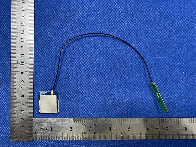
Click to zoom
Application Details
- Equipment Class
- DSS - Part 15 Spread Spectrum Transmitter
- Date of Grant
- Dec 05, 2022
- Application Purpose
- Original Equipment
- Date of Application
- Dec 05, 2022
- Equipment Note
- Dual-Band WiFi/Dual-Mode Bluetooth Module
- Frequency Range
- 2402.00000000 - 2480.00000000
- Company
- EJEK TECHNOLOGY CO.,LTD.
- Country
- China
Documents & Files
Document Text
Text extracted from the exhibit documents filed with the FCC. Open a document above to read the original.
Users Manual
S D P NAM SPEC. NO DATE:::: PRODUC A ME S O.:::: 2 T NA M APPROVE EJE SPEC 022.09.1 ME:::: ED CH K Te CIFI 14 AI004 0 ECKED chno ICAT REV 00 PREPA ology TION : 1. ARED y N 0 DCC ISSUUE AI00400 Datasheet EJEK Technology Co., Ltd. Proprietar y& Confidential Information 2 EJEK AI00400 WiFi 11a/b/g/n/ac & Bluetooth 5.0 Module Data Sheet AI00400 Datasheet EJEK Technology Co., Ltd. Proprietar y& Confidential Information 3 Revision History Date Revision Content Revised By Version 2022/09/14 - Preliminary Eric 1.0 AI00400 Datasheet EJEK Technology Co., Ltd. Proprietar y& Confidential Information 4 Contents 1. Introduction .......................................................................................................... 5 2. Features ................................................................................................................ 6 3. General Specification ........................................................................................... 7 3.1 General Specification ........................................................................................ 7 3.2 Voltages ............................................................................................................... 7 4. Wi-Fi RF Specification .......................................................................................... 8 4.1 2.4GHz RF Specification ................................................................................. 8 4.2 5GHz RF Specification ....................................................................................... 9 5. Bluetooth Specification ..................................................................................... 11 5.1 Bluetooth Specification .................................................................................... 11 6. Pin Assignments ................................................................................................... 12 6.1 Pin Outline ..................................................................................................... 12 6.2 Pin Definition ................................................................................................. 12 7. External clock reference .................................................................................... 14 8. Host Interface Timing Diagram .......................................................................... 15 8.1 Power-up Sequence Timing Diagram ........................................................... 15 8.2 SDIO Pin Description ................................................................................... 16 8.3 PCM Interface Description ............................................................................ 21 8.4 UART Interface Description .......................................................................... 25 9. Recommended Reflow Profile ........................................................................... 27 AI00400 Datasheet EJEK Technology Co., Ltd. Proprietar y& Confidential Information 5 1. Introduction EJEK Technology would like to announce a performance and low-power consumption module which has all of the Wi-Fi, Bluetooth functionalities. The highly integrated module makes the possibilities of web browsing, VoIP, Bluetooth headsets applications. With seamless roaming capabilities and advanced security, also could interact with different vendors’ 802.11a/b/g/n/ac Access Points in the wireless LAN. The wireless module complies with IEEE 802.11a/b/g/n/ac standard to connect to the wireless LAN. The integrated module provides SDIO interface for Wi-Fi, UART / PCM interface for Bluetooth. This compact module is a total solution for a combination of Wi-Fi + BT technologies. The module is specifically developed for Smart console and electronic devices which with IoT function. EJ 2. • • • • • • • • • • A JEK Techno Feature • IEEE 8 • TX and • Single- • Suppor • Suppor and W maintai • Suppor - SD • BT hos - UA - PC • Compli future • Suppor allowin • Adaptiv A simplified ology Co., Lt es 02.11a/b/g d RX low-de -stream spa rts 20, 40, 8 rts 1antenn WLAN rece ining excel rts standar DIO v3.0(4- st digital int ART (up to CM for audi es with Bl u specificatio rts extende g for retra ve frequenc block diag td. g/n/ac dua ensity parit atial multip 80 MHz ch na with on ive signal llent sensit d SDIO v3 -bit) — up t erface: 4 Mbps) o data uetooth Co ons. With B ed synchro ansmission cy hopping gram of the l-band radi ty check (L plexing up t hannels wit e for WLA path elimi tivity for bo .0 and bac to 208 MHz ore Specifi Bluetooth C onous conn of dropped g (AFH) for e module is io with virtu LDPC) sup to 433.3 M th optional AN & Bluet inates the oth Bluetoo ckward com z clock rate cation Ver Class 1 or nections (e d packets. r reducing r s depicted Prop ual-simulta pport for im bps data r SGI (256 Q ooth share need for oth and WL mpatible wit e in SDR10 rsion 5.0 w Class2 tran eSCO), for radio frequ in the figu r rietary&Con neous dua proved ran ate. QAM modu ed port. Als an externa AN. th SDIO v2 04 mode with provisio nsmitter op r enhanced ency interf re below. AI00400 nfidential Info al-band ope nge and po ulation) so, shared al power s 2.0 host int ons for su peration. d voice qu ference. 0 Datash ormation eration ower efficie d Bluetooth splitter whi erfaces. pporting uality by 6 heet ency. h ile 7 AI00400 Datasheet EJEK Technology Co., Ltd. Proprietar y& Confidential Information 3. General Specification 3-1. General Specification Model Name AI00400 Product Description 1Tx/1Rx 802.11 a/b/g/n/ac Wi-Fi + BT 5.0 Module Dimension L x W x H: 37.6(inc. pin) x 36.6 x 7.3 (typical) mm WiFi Interface SDIO v2.0/v3.0 BT Interface UART / PCM Operating temperature -30°C to 85°C Storage temperature -40°C to 125°C Humidity Operating Humidity 10% to 95% Non-Condensing 3-2. Voltages 3-2-1. Absolute Maximum Ratings Symbol Description Min. Max. Unit WIFI-VCC Input supply Voltage -0.5 5 V VCC-IO-WIFI Digital/Bluetooth/SDIO/ I/O Voltage -0.5 3.9 …
Text truncated - open the document above for the full version.
Attestation Statements
EJEK TECHNOLOGY CO.,LTD. Request for Modular/Limited Modular Approval Date: December 5, 2022 Subject: Manufacturer’s Declaration for ☒ - Modular Approval ☐ - Split Modular Approval ☐ - Limited Modular Approval ☐ - Limited Split Modular Approval Confidentiality Request for: _____FCC ID:_2A9G7AI00400______ 8 Basic Requirements – FCC Part 15.212(a)(1) For Items Marked “NO(*)”, the Limited Module Description Must be Filled Out on the Following Pages Modular Approval Requirement Requirement Met 1. The modular transmitter must have its own RF shielding. This is intended to ensure that the module does not have to rely upon the shielding provided by the device into which it is installed in order for all modular transmitter emissions to comply with FCC limits. It is also intended to prevent coupling between the RF circuitry of the module and any wires or circuits in the device into which the module is installed. Such coupling may result in non-compliant operation. The physical crystal and tuning capacitors may be located external to the shielded radio elements. 15.212(a)(1)(i) ☒ - YES ☐ - NO(*) Details: <example – The module contains a metal shield which covers all RF components and circuitry. The shield is located on the top of the board next to antenna connector> 2. The modular transmitter must have buffered modulation/data inputs (if such inputs are provided) to ensure that the module will comply with FCC requirements under conditions of excessive data rates or over-modulation. 15.212(a)(1)(ii) ☒ - YES ☐ - NO(*) Details: <example – Data to the modulation circuit is buffered as described in the operational description provided with the application> 3. The modular transmitter must have its own power supply regulation on the module. This is intended to ensure that the module will comply with FCC requirements regardless of the design of the power supplying circuitry in the device into which the module is installed. 15.212(a)(1)(iii) ☒ - YES ☐ - NO(*) Details: <example – The module contains its own power supply regulation. Please refer to schematic filed with this application> 4. The modular transmitter must comply with the antenna and transmission system requirements of §§ 15.203, 15.204(b), 15.204(c), 15.212(a), and 2.929(b). The antenna must either be permanently attached or employ a ‘‘unique’’ antenna coupler (at all connections between the module and the antenna, including the cable). The ‘‘professional installation’’ provision of § 15.203 is not applicable to modules but can apply to limited modular approvals under paragraph 15.212(b). 15.212(a)(1)(iv) ☒ - YES ☐ - NO(*) Details: <example – The module connects to its antenna using an UFL connector which is considered a non-standard connector. A list of antennas tested and approved with this device may be found in users manual provided with the application> 5. The modular transmitter must be tested in a stand-alone configuration, i.e., the module must not be inside another device during testing. This is intended to demonstrate that the module is capable of complying with Part 15 emission limits regardless of the device into which it is eventually installed. Unless the transmitter module will be battery powered, it must comply with the AC line conducted requirements found in Section 15.207. AC or DC power lines and data input/output lines connected to the module must not contain ferrites, unless they will be marketed with the module (see Section 15.27(a)). The length of these lines shall be length typical of actual use or, if that length is unknown, at least 10 centimeters to insure that there is no coupling between the case of the module and supporting equipment. Any accessories, peripherals, or support equipment connected to the module during testing shall be unmodified or commercially available (see Section 15.31(i)). 15.212(a)(1)(v) ☒ - YES ☐ - NO(*) Details: <example – The module was tested stand-alone as shown in test setup photographs filed with this application> EJEK TECHNOLOGY CO.,LTD. Modular Approval Requirement Requirement Met 6. The modular transmitter must be labeled with its own FCC ID number, or use an electron display (see KDB Publication 784748). If using a permanently affixed label with its own FCC ID number, if the FCC ID is not visible when the module is installed inside another device, then the outside of the device into which the module is installed must also display a label referring to the enclosed module. This exterior label can use wording such as the following: “Contains Transmitter Module FCC ID: XYZMODEL1” or “Contains FCC ID: XYZMODEL1.” Any similar wording that expresses the same meaning may be used. The Grantee may either provide such a label, an example of which must be included in the application for equipment authorization, or, must provide adequate instructions along with the module which explain this requirement. In the latter case, a copy of these instructions must be included in the application for equipment authorization. If the modular transmitter uses an electronic display of the FCC identification number, the information must be readily accessible and visible on the modular transmitter or on the device in which it is installed. If the module is installed inside another device, then the outside of the device into which the module is installed must display a label referring to the enclosed module. This exterior label can use wording such as the following: “Contains FCC certified transmitter module(s).” Any similar wording that expresses the same meaning may be used. The user manual must include instructions on how to access the electronic display. A copy of these instructions must be included in the application for equipment authorization. 15.212(a)(1)(vi) ☒ - YES ☐ - NO(*) Details: <example – There is a label on the module as shown in the labeling exhibit filed with this application. Host specific labeling instructions are shown in the installation manual .filed with this application.> 7. The modular tr…
Text truncated - open the document above for the full version.
Cover Letter(s)
EJEK TECHNOLOGY CO.,LTD. 12/04/2022 Eurofins Electrical and Electronic Testing NA, Inc. 914 West Patapsco Avenue Baltimore, MD 21230 RE: CONFIDENTIALITY REQUEST FOR (Dual-Band WiFi/Dual-Mode Bluetooth Module /# AND FCC ID: 2A9G7AI00400) To Whom It May Concern: This letter serves as an official request for confidentiality under sections 0.457 and 0.459 of CFR 47. We have requested that the - Block Diagram - Schematics - Operational Description --SOFTWARE SECURITY REQUIREMENTS FOR U-NII DEVICES required to be submitted with this application be permanently withheld from public review. The above documents are company proprietary information that could never get into the possession of your competition. Please contact me if there is any information you may need. Sincerely, Client’s signature: Client’s name / title : Antony Fu/ PM Contact information / address: No. 106, Zhongshan 3rd Rd., Daya Dist., Taichung City 428, Taiwan (R.O.C.)
Cover Letter(s)
EJEK TECHNOLOGY CO.,LTD. 12/04/2022 Eurofins Electrical and Electronic Testing NA, Inc. 914 West Patapsco Avenue Baltimore, MD 21230 RE: LETTER OF AGENT AUTHORIZATION To Whom It May Concern: We, the undersigned, hereby authorize (Shenzhen CTA Testing Technology Co., Ltd.) to act on our behalf in all matters relating to application for equipment authorization, including the signing of all documents relating to these matters. We also hereby certify that no party to the application authorized hereunder is subject to the denial of benefits, including FCC benefits, pursuant to Section 5301 of the Anti-Drug Abuse Act of 1988, 21 U.S.C.853(a). This agreement expires one year from the current date. Sincerely, Client’s signature: Client’s name / title : Antony Fu/ PM Contact information / address: No. 106, Zhongshan 3rd Rd., Daya Dist., Taichung City 428, Taiwan (R.O.C.)
External Photos
Antenna
ID Label/Location Info
LABEL FOR MODULE EJEK AI00400 FCC ID: 2A9G7AI00400 IC: 29756-AI00400
Test Report
Antenna Specification Manufactory: Shenzhen Cheung Bo a Technology Co., Ltd. MODEL : XBY20170262 TYPE: PCB ANTENNA Characteristic: Frequency: WIFI 2.4G~2.5G/5.15G~5.8G ANTENNA Material: PCB Gain(Peak): 2dBi Cable Type: O.D 1.13mm Connector: IPEX I TEST DATA: Antenna
Test Report
Report No.: CTA22111600702 Page 33 of 44 Shenzhen CTA Testing Technology Co., Ltd. Room 106, Building 1, Yibaolai Industrial Park, Qiaotou Community, Fuhai Street, Bao’an District, Shenzhen, China Tel:+86-755 2322 5875 E-mail:[email protected] Web:http://www.cta-test.cn GFSK(CH00) GFSK(CH39) reference reference 30MHz-1G 30MHz-1G 1G-25G 1G-25G Report No.: CTA22111600702 Page 34 of 44 Shenzhen CTA Testing Technology Co., Ltd. Room 106, Building 1, Yibaolai Industrial Park, Qiaotou Community, Fuhai Street, Bao’an District, Shenzhen, China Tel:+86-755 2322 5875 E-mail:[email protected] Web:http://www.cta-test.cn GFSK(CH78) π/4DQPSK (CH00) reference reference 30MHz-1G 30MHz-1G 1G-25G 1G-25G Report No.: CTA22111600702 Page 35 of 44 Shenzhen CTA Testing Technology Co., Ltd. Room 106, Building 1, Yibaolai Industrial Park, Qiaotou Community, Fuhai Street, Bao’an District, Shenzhen, China Tel:+86-755 2322 5875 E-mail:[email protected] Web:http://www.cta-test.cn π/4DQPSK (CH39) π/4DQPSK (CH78) reference reference 30MHz-1G 30MHz-1G 1G-25G 1G-25G Report No.: CTA22111600702 Page 36 of 44 Shenzhen CTA Testing Technology Co., Ltd. Room 106, Building 1, Yibaolai Industrial Park, Qiaotou Community, Fuhai Street, Bao’an District, Shenzhen, China Tel:+86-755 2322 5875 E-mail:[email protected] Web:http://www.cta-test.cn 8DPSK (CH00) 8DPSK (CH39) reference reference 30MHz-1G 30MHz-1G 1G-25G 1G-25G Report No.: CTA22111600702 Page 37 of 44 Shenzhen CTA Testing Technology Co., Ltd. Room 106, Building 1, Yibaolai Industrial Park, Qiaotou Community, Fuhai Street, Bao’an District, Shenzhen, China Tel:+86-755 2322 5875 E-mail:[email protected] Web:http://www.cta-test.cn 8DPSK (CH78) reference 30MHz-1G 3G-25G Report No.: CTA22111600702 Page 38 of 44 Shenzhen CTA Testing Technology Co., Ltd. Room 106, Building 1, Yibaolai Industrial Park, Qiaotou Community, Fuhai Street, Bao’an District, Shenzhen, China Tel:+86-755 2322 5875 E-mail:[email protected] Web:http://www.cta-test.cn Band-edge Measurements for RF Conducted Emissions: GFSK Left Band edge hoping off Right Band edge hoping off Left Band edge hoping on Right Band edge hoping on Report No.: CTA22111600702 Page 39 of 44 Shenzhen CTA Testing Technology Co., Ltd. Room 106, Building 1, Yibaolai Industrial Park, Qiaotou Community, Fuhai Street, Bao’an District, Shenzhen, China Tel:+86-755 2322 5875 E-mail:[email protected] Web:http://www.cta-test.cn π/4DQPSK Left Band edge hoping off Right Band edge hoping off Left Band edge hoping on Right Band edge hoping on
Test Report
Report No.: CTA22111600702 Page 40 of 44 Shenzhen CTA Testing Technology Co., Ltd. Room 106, Building 1, Yibaolai Industrial Park, Qiaotou Community, Fuhai Street, Bao’an District, Shenzhen, China Tel:+86-755 2322 5875 E-mail:[email protected] Web:http://www.cta-test.cn 8DPSK Left Band edge hoping off Right Band edge hoping off Left Band edge hoping on Right Band edge hoping on Report No.: CTA22111600702 Page 41 of 44 Shenzhen CTA Testing Technology Co., Ltd. Room 106, Building 1, Yibaolai Industrial Park, Qiaotou Community, Fuhai Street, Bao’an District, Shenzhen, China Tel:+86-755 2322 5875 E-mail:[email protected] Web:http://www.cta-test.cn 4.9 Pseudorandom Frequency Hopping Sequence TEST APPLICABLE For 47 CFR Part 15C section 15.247 (a) (1) requirement: Frequency hopping systems shall have hopping channel carrier frequencies separated by a minimum of 25 kHz or the 20 dB bandwidth of the hop-ping channel, whichever is greater. Alternatively, frequency hopping systems operating in the 2400–2483.5 MHz band may have hopping channel carrier frequencies that are separated by 25 kHz or two-thirds of the 20 dB bandwidth of the hopping channel, whichever is greater, provided the systems operate with an output power no greater than 125 mW. The system shall hop to channel frequencies that are selected at the system hopping rate from a pseudo randomly ordered list of hopping frequencies. Each frequency must be used equally on the average by each transmitter. The system receivers shall have input bandwidths that match the hop-ping channel bandwidths of their corresponding transmitters and shall shift frequencies in synchronization with the transmitted signals. EUT Pseudorandom Frequency Hopping Sequence Requirement The pseudorandom frequency hopping sequence may be generated in a nice-stage shift register whose 5 th and 9 th stage outputs are added in a modulo-two addition stage. And the result is fed back to the input of the first stage. The sequence begins with the first one of 9 consecutive ones, for example: the shift register is initialized with nine ones. ● Number of shift register stages:9 ● Length of pseudo-random sequence:29-1=511 bits ● Longest sequence of zeros:8(non-inverted signal) An example of pseudorandom frequency hopping sequence as follows: Each frequency used equally one the average by each transmitter. The system receiver have input bandwidths that match the hopping channel bandwidths of their corresponding transmitter and shift frequencies in synchronization with the transmitted signals. Report No.: CTA22111600702 Page 42 of 44 Shenzhen CTA Testing Technology Co., Ltd. Room 106, Building 1, Yibaolai Industrial Park, Qiaotou Community, Fuhai Street, Bao’an District, Shenzhen, China Tel:+86-755 2322 5875 E-mail:[email protected] Web:http://www.cta-test.cn 4.10 Antenna Requirement Standard Applicable For intentional device, according to FCC 47 CFR Section 15.203, an intentional radiator shall be designed to ensure that no antenna other than that furnished by the responsible party shall be used with the device. And according to FCC 47 CFR Section 15.247 (c), if transmitting antennas of directional gain greater than 6dBi are used, the power shall be reduced by the amount in dB that the directional gain of the antenna exceeds 6dBi. Refer to statement below for compliance The manufacturer may design the unit so that the user can replace a broken antenna, but the use of a standard antenna jack or electrical connector is prohibited. Further, this requirement does not apply to intentional radiators that must be professionally installed. Antenna Connected Construction The maximum gain of antenna was 2.00 dBi. Remark:The antenna gain is provided by the customer , if the data provided by the customer is not accurate, Shenzhen CTA Testing Technology Co., Ltd. does not assume any responsibility. Report No.: CTA22111600702 Page 43 of 44 Shenzhen CTA Testing Technology Co., Ltd. Room 106, Building 1, Yibaolai Industrial Park, Qiaotou Community, Fuhai Street, Bao’an District, Shenzhen, China Tel:+86-755 2322 5875 E-mail:[email protected] Web:http://www.cta-test.cn 5 T e s t S e t u p P h o t o s o f t h e E U T Report No.: CTA22111600702 Page 44 of 44 Shenzhen CTA Testing Technology Co., Ltd. Room 106, Building 1, Yibaolai Industrial Park, Qiaotou Community, Fuhai Street, Bao’an District, Shenzhen, China Tel:+86-755 2322 5875 E-mail:[email protected] Web:http://www.cta-test.cn 6 P h o t o s o f t h e E U T Reference to the test report No. CTA22111600701 ********************** End of Report **********************
Contact Information
Applicant
Antony Fu
Technical Contact
Shenzhen CTA Testing Technology Co., Ltd.Eric Wang
[email protected]+86 755 2322 5875
Room 106, Building 1, Yibaolai Ind. Park · Shenzhen · China
Test Firm
SHENZHEN CTA TESTING TECHNOLOGY CO., LTD.Eric Wang
[email protected]+86 755 2322 5875
Technical Specifications
| # | Rule Parts | Frequency Range | Power Output |
|---|---|---|---|
| 1 | 15C | 2.40 GHz - 2.48 GHz | 369.00 µW |
Other Applications from EJEK TECHNOLOGY CO.,LTD.
2A9G7WTM1C10
Jun 05, 2023Wireless Power Transmitter
Equipment Class
DCD - Part 15 Low Power Transmitter Below 1705 kHz