2AA9G-1116Baby Monitor
STARIAN TECHNOLOGY LIMITED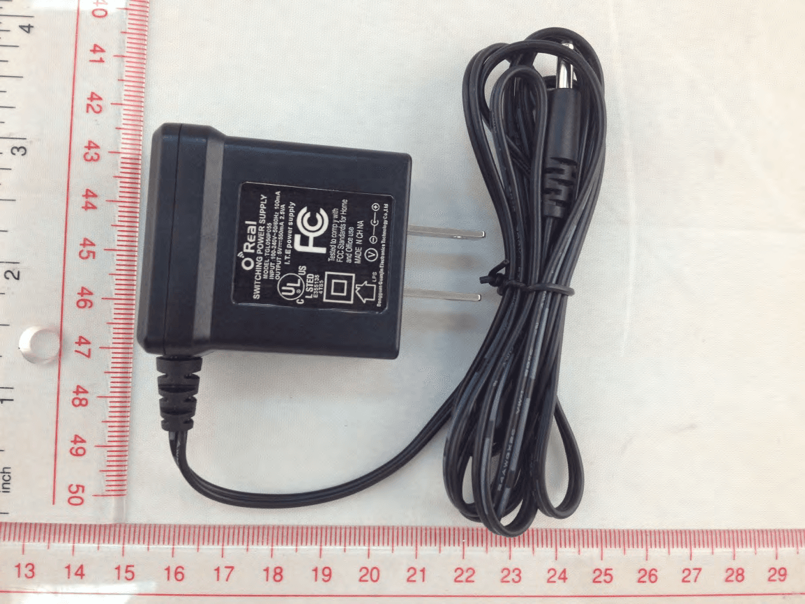
Click to zoom
Application Details
- Equipment Class
- DTS - Digital Transmission System
- Date of Grant
- Jan 15, 2015
- Application Purpose
- Original Equipment
- Date of Application
- Jan 15, 2015
- Equipment Note
- Baby Monitor
- Frequency Range
- 2413.00000000 - 2468.00000000
- Company
- STARIAN TECHNOLOGY LIMITED
- Country
- China
Documents & Files
Document Text
Text extracted from the exhibit documents filed with the FCC. Open a document above to read the original.
Users Manual
INSTRUCTION MANUAL Model:ABM1116 (#28700-114) 1. Packing List a) 1 x PU (PARENT) Receiver b) 1 x BU (BABY) Transmitter c) 2 x AC adaptors (5V/550mA ) d) 2 x AA Rechargeable battery (1.2V 1100 mAH) e) 1 x User Manual 2. Overview of product 2.1 PU(PARENT) 2.2 BU (BABY) ②MIC ③Power button ④Power Indicator ⑤ DC IN ⑥ Temperature Sensor ○ 13 DC IN ○ 1 LCD ○ 8 Power Indicator ○ 10 Belt clip ○ 11 Battery cover ○ 5 Power button ○ 9 Speaker ○ 12 Call key ○ 2 Volume Indicator ①LED Len ○ 7 Volume down ○ 3 Function keys ○ 4 Volume up ○ 6 Communication LED 3. Start to use 3.1 PU receiver instructions a. Disassemble the battery cover. Insert two AA rechargeable batteries (ensure the polarity of the batteries is right). Assembly the battery cover. Note: Use rechargeable battery or AC adaptor as power supply. b. Press the Power button for 3 seconds to power up, and the Power Indicator is on. c. When battery voltage is lower than 2.2V, the low battery voltage alarm (BB sounds) appear once. When battery voltage is lower than 2.1V, the low battery voltage alarm (BB sounds) appear continuously then follow by the Power Indicator off. Note: The battery should recharge when the low battery voltage alarm appear. d. In the process of charging , the top left comer of the LCD battery symbol is flashing ,it is charging. When the battery Symbol motionless and to full case shows that is has enough power. e. When PU is idle, the Volume Indicator is off and the communication LED is flashing. . f. When PU is connected with BU, the communication LED is on. 3.2 BU transmitter instructions a. Connect the AC adaptor (5V/550mA) b. Press the Power button for 3 seconds, the Power Indicator is on. c. Press the Power button to change channel (a total of 12 channels can be changed) 4. Communication Function a. When PU power on, press the volume up and down keys together. Display will appear “ID”. Then power on the BU, PU can receive signal transmitted from BU in 5 seconds b. PU volume indicator will be on when receiving signal. The greater the volume received from BU, the more the volume LED will be on (maximum 5 LEDs will be on). c. Default volume setting in PU is level 3 (maximum: 5 levels). d. User can adjust the volume by pressing the volume up/down button in PU. e. When PU unable to receive signal from BU, the communication LED keeps flashing. When PU receive signal from BU, the communication LED keeps on. g. When press call key, PU can speak to BU (Talk back). h. Communication distance of PU and BU: i. Outdoor range can up to 300m ii. Indoor range depends on the status of RF interference Note: Switch off PU receiver when it is not in use. 5. Function keys in PU a. Music: When PU is in connection with BU, press Music key can play lullaby (2 lullabies is default) both in PU and BU. A Music sign will appear in LCD.. b. Temperature: BU can detect temperature and will transmit information to PU and display. Press Temperature key can switch the temperature display in C (Celsius) or F (Fahrenheit). Note: When the temperature is higher than 32°C, the LCD will display “HH”, When the temperature is less than 15°C, the LCD will display “LL”. c. Backlight: Press the backlight key can switch on the backlight in BU. A Backlight sign will appear in LCD. Press again can switch off the backlight 6. Problem diagnosis and troubleshooting Reasons for PU that cannot receive BU signal: a. Whether power supply plug in properly for BU, . b. Whether BU is in off mode c. Whether there are nearby interference (WIFI or other device). Press the Power button on BU that can switch to another available channel. d. Whether there are many interference exists and/or devices are out of range. Reasons for Function key failure: a. Whether PU is battery low b. Whether BU is in off mode c. Whether PU is not connected with BU d. Whether there are many interference exists and/or devices are out of range. 7. Product parameters 7.1 PU Receiver a. Receiver Frequency: 2.4G b. Frequency: 12 channels (CH1:2413MH, CH2:2418MHZ, CH3:2423MHZ, CH4:2428MHZ, CH5:2433MHZ, CH6:2438MHZ, CH7:2443MHZ, CH8:2448MHZ, CH9:2453MHZ, CH10:2458MHZ, CH11:2463MHZ, CH12:2468MHZ) c. Power supply: AC110~240V, DC IN: 5V 2W, Current consumption: 400mA d. Operating Temperature: 0°C~40°C/ 32°F~104°F e. Battery life: 12 hours PU Receiver complies with part 15 of the FCC rules. Operation is subject to the following two conditions: (1) this device may not cause harmful interference, and (2) this device must accept any interference received, including interference that may cause undesired operation. NOTE: The manufacturer is not responsible for any radio or TV interference caused by unauthorized modifications to this equipment. Such modifications could void the user’s authority to operate the equipment. NOTE: This equipment has been tested and found to comply with the limits for a Class B digital device, pursuant to part 15 of the FCC Rules. These limits are designed to provide reasonable protection against harmful interference in a residential installation. This equipment generates uses and can radiate radio frequency energy and, if not installed and used in accordance with the instructions, may cause harmful interference to radio communications. However, there is no guarantee that interference will not occur in a particular installation. If this equipment does cause harmful interference to radio or television reception, which can be determined by turning the equipment off and on, the user is encouraged to try to correct the interference by one or more of the following measures: - Reorient or relocate the receiving antenna. - Increase the separation between the equipment and receiver. -Connect the equipment into an outlet on a circuit different from that to which the receiver is connected. -Consult the dealer or an experienced radio/TV technician for help Additional information on Specific Absorption Rates (SAR) can be found on the FCC website at (http://www.fcc.gov/encyclopedia/radio-frequency-safety) …
Text truncated - open the document above for the full version.
Cover Letter(s)
Date: Dec 30, 2014 To : Federal Communications Commission, Authorization & Evaluation Division, 7435 Oakland Mills Road, Columbia, MD 21046 To Whom It May Concern: The STARIAN TECHNOLOGY LIMITED, the undersigned, hereby authorizes Mr. Wu Xuewen from Shenzhen BALUN Technology Co.,Ltd., to act on the behalf of the STARIAN TECHNOLOGY LIMITED solely in matters relating to the application for an FCC equipment authorization for FCC ID: 2AA9G-1116 including the signing of documents in connection with this Application. Necessary acts carried out by Shenzhen BALUN Technology Co.,Ltd. on our behalf of the STARIAN TECHNOLOGY LIMITED in connection with the Application shall have the same effect as acts of the STARIAN TECHNOLOGY LIMITED. The STARIAN TECHNOLOGY LIMITED also hereby certify that no party to this application is subject to a denial of benefits, including FCC benefits, pursuant to Section 5301 of the Anti-Drug Abuse Act of 1988, 21 U.S.C. 853(a). Thank you for your attention to this matter. Yo urs Sincerely, He Yun Ren QC Manager
Cover Letter(s)
Date: Dec 30, 2014 To: Federal Communications Commission, Authorization & Evaluation Division, 7435 Oakland Mills Road, Columbia, MD 21046 Re: STARIAN TECHNOLOGY LIMITED FCC ID: 2AA9G-1116 FCC Part 15C Certification Confidentiality Request Gentlemen: This letter is to comply with 47 CFR 0.457 and 0.459 pertaining to confidentiality material. STARIAN TECHNOLOGY LIMITED requests that the following documents regarding this submission for FCC ID: 2AA9G-1116 be kept confidential: Exhibit Type File Name Block Diagram Block Diagram.pdf Schematics Schematics.pdf Operational Description Operational Description.pdf Those documents contain detailed system and equipment description and related information about the product which STARIAN TECHNOLOGY LIMITED considers to be confidential proprietary, a custom design and, otherwise, not releasable to the general public. Since this design is a basis form which future technological products will evolve, STARIAN TECHNOLOGY LIMITED considers this information would be of benefit to its competitors, and that the disclosure of the information in these documents would give competitors an unfair advantage in the market. Yours Sincerely, He Yun Ren QC Manager
External Photos
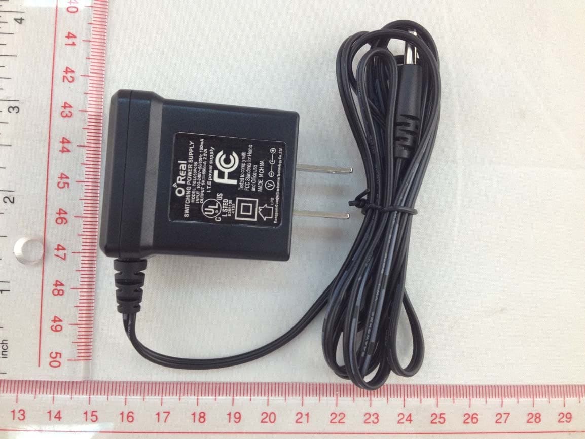
Report No.: BL-SZ14B0095-601 49 ANNEX C EUT PHOTOS C.1 Appearance of the EUT THE FRONT OF PARENT THE BACK OF PARENT Report No.: BL-SZ14B0095-601 50 THE DOWN OF PARENT THE UP OF PARENT Report No.: BL-SZ14B0095-601 51 THE LEFT OF PARENT THE RIGHT OF PARENT Report No.: BL-SZ14B0095-601 55 THE CHARGER
ID Label/Location Info
Label Label Location
Internal Photos
Report No.: BL-SZ14B0095-601 56 C.2 Inside of the EUT PARENT UNCOVER VIEW 1 PARENT UNCOVER VIEW 2 Report No.: BL-SZ14B0095-601 57 PARENT BOARD TOP VIEW 1 PARENT BOARD BACK VIEW 1 Report No.: BL-SZ14B0095-601 58 PARENT BOARD TOP VIEW 2 PARENT BOARD TOP VIEW 3 Dipole Antenna
Parts List/Tune Up Info
S1116P-1.4 BOM 2014/8/25 Item Qty ReferencePart NameVALUEDescriptionManufacturer 11C37CCAP04020.5p 21C58CCAP04020.5p 3 2 C2 C11 CCAP04020.5p 41C38CCAP04021p 5 1 C32CCAP04021p 6 2 C33 C60CCAP0402nc 7 1 C12CCAP04023p 8 1 C36CCAP04026.8p 9 2 C80 C47CCAP040210p 10 1 C45CCAP040222p 11 2 C3-4CCAP040227p 12 1 C21CCAP040239p 13 4 C6 C13 C17 C22CCAP040247p 14 1 C81CCAP0402100p 15 2 C50 C40CCAP0402220p 16 5 C104 C39 C76 C77 C55CCAP04021n 17 5 C7 C16 C20 C59 C67CCAP040210n 18 10 C15 C34 C1 C82 C51 C49 C52 C53 C42 C43 CCAP0402100n 19 6 C5 C14 C23 C25 C27 C41CCAP0402100n 20 3 C10 C18 C44CCAP06031uF 21 7 C9 C19 C24 C30-31 C97 C151 CCAP06031uF 22 2 C46 C54CCAP080510uF 23 2 C35 C8ECAP220uF/6.3V 24 2 C26 C28ECAP220uF/6.3V 25 1 C48CCAP0603nc 26 1 C29 CCAP0402nc 27 1 FB1FB06031000 28 1 FB2FB06031000 29 1L3IND04022.2nH 30 1L8IND04022.2nH 31 1L6IND04021.8nH 32 3 L4-5 L7IND04026.2nH 33 2 L10-11IND08054.7uH 34 1 L2IND18124.7uH 35 1 LED1LED-DIPGREEN 36 1 LED2LED-DIPGREEN 37 5 LED3-7LED-DIPGREEN 38 1 LED8LED-DIP Back light for LED Yellow 39 1 D1DIODELL4148 40 2 D4 D5DIODELL4148 41 2 D2-3DIODELL4148 42 1 Q1TRANSISTORBCX51 43 1 Q2TRANSISTORDTC143EE 44 1Q3RES04020R 45 1 Q4MOSFET-PCES2321 46 1 R23RES121010R 47 1 R28RES040210R 48 1 R22 RES0402470R 49 11 R1-4 R6-8 R11 R27 R18 R29 RES04021k 50 1 R15RES04022.2k 51 1 R32RES0402100R 52 2 R46 R20RES040210K 53 2 R24 R34RES040247K 54 6 R9 R12 R10 R21 R31 R30RES0402100K 55 6 R5 R13-14 R17 R25 R33RES0402100k 56 1 R19RES0402470k 57 2 R16 R26RES0402100k 58 1 R68RES0402100K 59 1 R45RES0402191K 60 1 MICMICDIP6027 61 1 SP1SPEAKERSPEAKER 62 1 U1(同ABM1112)ICRF IC 63 1 U6(同ABM1112)ICMCU 64 1 U2ICUP0108AMA3-33 65 1 U7ICUP0108AMA5-33 66 1 U3ICRFX2401C 67 1 U4ICHT67F40 68 1 U5ICMP3410 69 1 LCDLCD 111635*22.8*2.8 70 1 XT1XTAL32M 71 1 ANT1Antenna Brass, 30.5*6.5mm Ø1.2, Ni-plated 72 1 DC1DC-JKDS413 73 1 SW7Tact Switch for talk back7.3*6.5*4.5 74 1 S1116P-1.4 PCB 2 layer54.3*42mm
Parts List/Tune Up Info
Rated RF power output: Mode The Tune-up power range(Customer Declared)(dBm) Range(dBm) DSSS(IEEE 802.15.4) 12.50±1.20 11.30~13.70 Note: These appropriate rated RF output power settings are stored in each device individually. The user has no possibility to change these settings later on, and during manufacturing each device will be individual calibrated. The measurement is done in fully calibrated setup, which is based on the base station simulator. Furthermore, the highest power level is verified afterwards in a call measurement on three channels(low, middle and high).
Test Report
Report No.: BL-SZ14B0095-601 2 Revision History Version Issue Date Revisions Rev. 01 Dec 16, 2014 Initial Issue TABLE OF CONTENTS 1 ADMINISTRATIVE DATA (GENERAL INFORMATION) ........................................................................ 5 1.1 Identification of the Testing Laboratory ............................................................................................ 5 1.2 Identification of the Responsible Testing Location ........................................................................... 5 1.3 Announce ........................................................................................................................................ 5 2 PRODUCT INFORMATION ................................................................................................................... 6 2.1 Applicant ......................................................................................................................................... 6 2.2 Manufacturer ................................................................................................................................... 6 2.3 General Description for Equipment under Test (EUT) ..................................................................... 6 2.4 Technical Information ...................................................................................................................... 7 2.5 Ancillary Equipment ......................................................................................................................... 7 3 SUMMARY OF TEST RESULTS ........................................................................................................... 8 3.1 Test Standards ................................................................................................................................ 8 3.2 Verdict ............................................................................................................................................. 8 3.3 Table for Carrier Frequency ............................................................................................................ 8 4 GENERAL TEST CONFIGURATIONS .................................................................................................. 9 4.1 Test Environments .......................................................................................................................... 9 4.2 Test Equipment List ......................................................................................................................... 9 4.3 Test Configurations ....................................................................................................................... 10 4.4 Description of Test Setup .............................................................................................................. 10 4.4.1 For Antenna Port Test ............................................................................................................ 10 4.4.2 For AC Power Supply Port Test .............................................................................................. 10 4.4.3 For Radiated Test (Below 30MHz) .......................................................................................... 11 4.4.4 For Radiated Test (30MHz-1GHz) .......................................................................................... 11 4.4.5 For Radiated Test (Above 1GHz) ........................................................................................... 12 4.5 Test Conditions ............................................................................................................................. 12 Report No.: BL-SZ14B0095-601 3 5 TEST ITEMS ....................................................................................................................................... 13 5.1 Antenna Requirements .................................................................................................................. 13 5.1. 1 Standard Applicable ............................................................................................................... 13 5.1.2 Antenna Anti-Replacement Construction ................................................................................ 13 5.1.3 Antenna Gain ......................................................................................................................... 13 5.2 Output Power ................................................................................................................................ 14 5.2.1 Test Limit ................................................................................................................................ 14 5.2.2 Test Procedure ....................................................................................................................... 14 5.3 6dB Bandwidth .............................................................................................................................. 15 5.3.1 Limit ........................................................................................................................................ 15 5.3.2 Test Procedure ....................................................................................................................... 15 5.4 Conducted Spurious Emission ...................................................................................................... 16 5.4.1 Limit ........................................................................................................................................ 16 5.4.2 Test Procedure ....................................................................................................................... 16 5.5 Conducted Emission ..................................................................................................................... 18 5.5.1 Limit ...........................................................................................................................…
Text truncated - open the document above for the full version.
Test Report
Report No.: BL-SZ14B0095-701 2 / 71 Revision History Version Issue Date Revisions Rev. 01 Jan. 9, 2015 Initial Issue TABLE OF CONTENTS 1 GENERAL INFORMATION ..................................................................................................................... 4 1.1 Identification of the Testing Laboratory ............................................................................................. 4 1.2 Identification of the Responsible Testing Location ............................................................................ 4 1.3 Test Environment Condition .............................................................................................................. 4 1.4 Announce .......................................................................................................................................... 4 2 PRODUCT INFORMATION ..................................................................................................................... 6 2.1 Applicant ........................................................................................................................................... 6 2.2 Manufacturer ..................................................................................................................................... 6 2.3 General Description for Equipment under Test (EUT) ...................................................................... 6 2.4 Technical Information ........................................................................................................................ 6 2.5 Ancillary Equipment .......................................................................................................................... 7 3 SUMMARY OF TEST RESULTS ............................................................................................................. 8 3.1 Test Standards .................................................................................................................................. 8 3.2 Device Category and SAR Limit ........................................................................................................ 8 3.3 Summary of SAR Value .................................................................................................................. 10 3.4 SAR Test Uncertainty ...................................................................................................................... 11 4 SAR MEASUREMENT SYSTEM ........................................................................................................... 13 4.1 Definition of Specific Absorption Rate (SAR) .................................................................................. 13 4.2 SATIMO SAR System ..................................................................................................................... 13 5 SYSTEM VERIFICATION ...................................................................................................................... 20 5.1 Antenna Port Test Requirement ...................................................................................................... 20 5.2 Purpose of System Check ............................................................................................................... 20 5.3 System Check Setup ....................................................................................................................... 20 5.4 System Verification Results(1g value) ............................................................................................ 21 6 EUT TEST POSITION CONFIGURATUONS ........................................................................................ 22 6.1 Head Exposure Conditions ............................................................................................................. 22 Report No.: BL-SZ14B0095-701 3 / 71 6.2 Body-worn Position Conditions ....................................................................................................... 23 6.3 Hotspot Mode Exposure Position Conditions .................................................................................. 24 7 SAR MEASUREMENT PROCEDURES ................................................................................................ 25 7.1 SAR Measurement Process Diagram ............................................................................................. 25 7.2 SAR Scan General Requirements .................................................................................................. 26 7.3 SAR Measurement Procedure ........................................................................................................ 27 7.4 Area & Zoom Scan Procedures ...................................................................................................... 27 7.5 PTT MEASUREMENT PROCEDURES .......................................................................................... 27 8 CONDUCTED RF OUPUT POWER ...................................................................................................... 28 9 SAR TEST RESULTS ............................................................................................................................ 29 9.1 Test result ....................................................................................................................................... 29 9.2 SAR Measurement Variability ......................................................................................................... 29 10 TEST EQUIPMENTS LIST .................................................................................................................... 31 11 REFERENCES ...................................................................................................................................... 32 ANNEX A SAR TEST RESULT OF SYSTEM VERIFICATION ................................................................. 33 ANNEX B SAR TEST SETUP PHOTOS ................................…
Text truncated - open the document above for the full version.
Test Setup Photos
Report No.: BL-SZ14B0095-601 46 ANNEX B TEST SETUP PHOTOS B.1 Conducted Test Photo B.2 Conducted Emissions Test Photo Report No.: BL-SZ14B0095-601 47 B.3 Radiated Test Photo Below 30MHz 30MHz to 1GHz Report No.: BL-SZ14B0095-601 48 Above 1GHz
Contact Information
Applicant
He Yun Ren
Test Firm
Shenzhen BALUN Technology Co.,Ltd.Xuewen Wu
Technical Specifications
| # | Rule Parts | Frequency Range | Power Output |
|---|---|---|---|
| 1 | 15C | 2.41 GHz - 2.47 GHz | 69.00 mW |
Other Applications from STARIAN TECHNOLOGY LIMITED
2AA9G-1150P
Jan 15, 2015Baby Monitor
Equipment Class
DTS - Digital Transmission System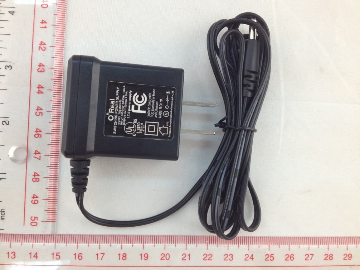
2AA9G-1116B
Jan 14, 2015Baby Monitor
Equipment Class
DTS - Digital Transmission System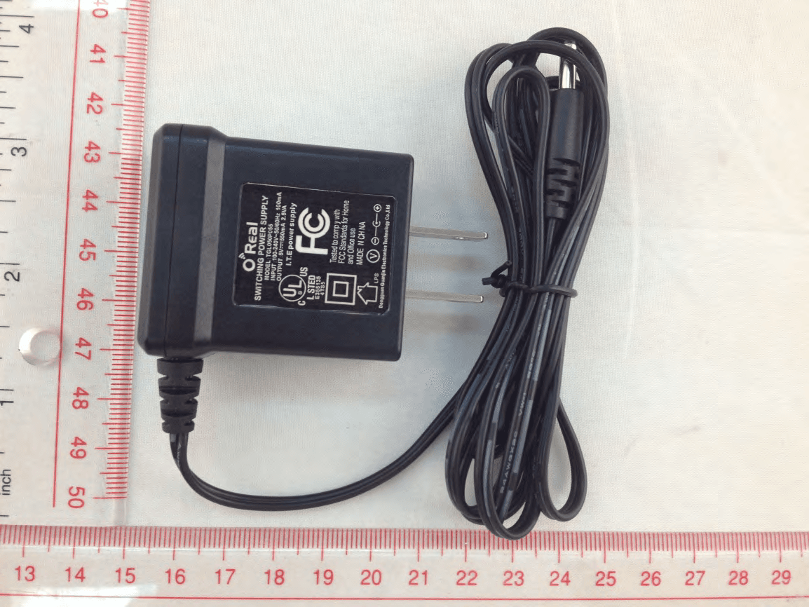
2AA9G-1150B
Jan 13, 2015Baby Monitor
Equipment Class
DTS - Digital Transmission System2AA9G-1112
Dec 22, 2013Baby Monitor
Equipment Class
DXX - Part 15 Low Power Communication Device Transmitter