2AAP8HSBT672.0 Speakers System
Guoguang Electric Co.,Ltd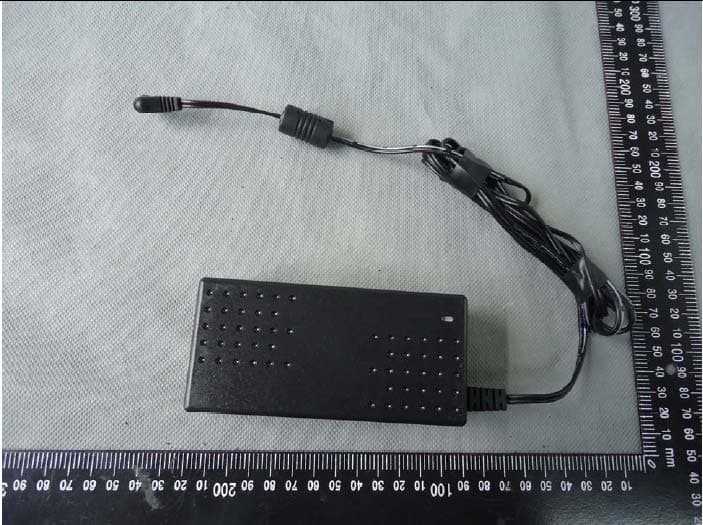
Click to zoom
Application Details
- Equipment Class
- DSS - Part 15 Spread Spectrum Transmitter
- Date of Grant
- Dec 12, 2013
- Application Purpose
- Original Equipment
- Date of Application
- Dec 12, 2013
- Equipment Note
- 2.0 Speakers System
- Frequency Range
- 2402.00000000 - 2480.00000000
- Company
- Guoguang Electric Co.,Ltd
- Country
- China
Documents & Files
Document Text
Text extracted from the exhibit documents filed with the FCC. Open a document above to read the original.
Users Manual
1. Read these instructions. 2. Keep these instructions. 3. Heed all warnings. 4. Follow all instructions. 5. Do not use this apparatus near water. 6. Clean only with a dry cloth 7. Do not block any ventilation openings. Install in accordance with the manufacturer’s instructions. 8. Do not install near any heat sources such as radiators, heat registers, stoves, or other apparatus (including amplifi ers) that produce heat. 9. Do not defeat the safety purpose of the polarized or grounding type plug. A polarized plug has two blades with one wider than the other. A grounding type plug has two blades and a third grounding prong. The wide blade or the third prong are provided for your safety. If the provided plug does not fi t into your outlet, consult an electrician for replacement of the obsolete outlet. 10. Protect the power cord from being walked on or pinched particularly at plugs, convenience receptacles, and the point where they exit from the apparatus. 11. Only use attachments/accessories specifi ed by the manufacturer. 12. Use only with the cart stand, tripod, bracket or table specifi ed by the manufacturer or sold with the apparatus. When a cart is used, use caution when moving the cart/ apparatus combination to avoid injury from tip-over. 13. Unplug this apparatus during lightning storms or when unused for long periods of time. NOTICE FOR THE SOUND BAR PLACEMENT Mounting the unit on a cabinet smaller than the length of the unit could result in an unstable position and the unit may tumble over, making a risk of personal injury, and damaging the product. Hitachi accepts no responsibility or liability for any injuries or property damage resulting from improper installation. For wall mounting Sound Bar, see online Owner’s Guide for details. YES NO 14. Refer all servicing to qualifi ed service personnel. Servicing is required when the apparatus has been damaged in any way, such as power-supply cord or plug is damaged, liquid has been spilled or objects have fallen into the apparatus, the apparatus has been exposed to rain or moisture, does not operate normally, or has been dropped. 15. WARNING: To reduce the risk of fi re or electric shock do not expose this apparatus to rain or moisture. 16. Do not allow the product to output distorted sound for an extended period of time. It may cause speaker overheating and fi re. 17. Sudden high volume sound may cause hearing or speaker damage. Turn sound bar volume down before connecting other devices. 18. Do not push objects through any opening in this unit, as they may touch dangerous voltage points that could result in fi re or electric shock. Never spill or spray any type of liquid into the unit. 19. Do not connect this unit to AC power using any device other than the supplied AC adaptor and AC cord. This could cause fi re, electrical shock, or damage. 20. Do not use with a voltage other than the power voltage specifi ed. This could cause fi re, electrical shock, or damage. Connect to 120VAC, 60Hz power only. 21. If you need to replace the supplied AC adapter or AC cord, contact the dealer from which you purchased the unit. 22. The Mains plug is used as the disconnect device, and shall remain readily operable. 23. Connect AC cord plug to properly grounded outlet. Thank you for purchasing the Hitachi Sound Bar. TECHNICAL SUPPORT AND IMPORTANT INFORMATION Remote ControlThe package includes the following items: HITACHI Sound Bar (Bluetooth ® connectivity)AC Adaptor, Audio Cable Quick Start Guide IMPORTANT SAFETY INSTRUCTIONS Model HSBT67 complete Owner’s Guide available at : www.hitachiserviceusa.com:8080/HSBT67.pdf Product Serial Number: Phone: 1.800.448.2244 (USA/CANADA) OR 01.800.703.0888 (MEXICO). Address: Hitachi America, Ltd. P.O. Box 99652 Troy, Michigan 48099 All specifications, features and dimensions are subject to change without notice. Refer to www.hitachi.us/tv for updates or more information. All trademarks are the property of their respective owners. © 2012 Hitachi America, Ltd. IMPORTANT PAIRING INFORMATION The Wireless Range is 33 feet. The HITACHI Sound Bar does NOT have a Bluetooth PASSCODE. Any PASSCODE request is for the source device (Phone, Tablet, Music Player). Display and Voice Cues LIMITED WARRANTY (VALID IN THE U.S.A., CANADA AND PUERTO RICO ONLY.) LIMITED WARRANTY TERMS AND CONDITIONS. Subject to the conditions and limitations set forth below, this HITACHI ® Sound Bar product (the “Product”) is warranted to be free from defects in materials and workmanship for a period of 1 year starting from the original date of purchase (the “Limited Warranty Period”) by the original purchaser (“Purchaser”). During the Limited Warranty Period, if the Product does not work properly due to a defect in materials or workmanship, Hitachi will, at Hitachi’s option, either: (i) repair the Product with new or refurbished parts, or (ii) replace the Product with a new or refurbished product with equal or greater features and functions as the Product. If Purchaser rejects, refuses or otherwise does not accept Hitachi’s repair or replacement off er, this Limited Warranty shall be void and of no further force or eff ect. This Limited Warranty extends to the Purchaser only and is not transferable. To qualify for coverage under this Limited Warranty, purchaser must notify Hitachi of a warranty claim during the Limited Warranty Period by calling 800.HITACHI and must provide a valid dated sales receipt for the Product. PARTS AND LABOR: There will be no charge for any replacement parts or labor during the Limited Warranty Period. Any replacement part used to repair the Product may be, at Hitachi’s option, a new or refurbished part, and such replacement part will be warranted only for 90 days or the remainder of the original 1-year Limited Warranty Period, whichever is longer. SERVICE LOCATIONS AND RETURNS: Products must be transported or shipped to a Hitachi-designated service facility (call 800.HITACHI for more information). Hitachi will not be respons…
Text truncated - open the document above for the full version.
External Photos
Page 1 of 5 External PHOTO: Model: HSBT67 Page 2 of 5 Page 3 of 5 Page 4 of 5 Page 5 of 5
ID Label/Location Info
Page 1 of 1 External PHOTO: Model: HSBT67 Attach label here
Internal Photos
Page 1 of 4 Internal PHOTO: Model: HSBT67 Page 2 of 4 Page 3 of 4 Page 4 of 4
Operational Description
Operational Description Product Description This product integrated a Bluetooth chipset to support the Bluetooth function that allows users to use it as a speaker as the primary usage of this device. The brief introduction of the circuit 1. The Bluetooth signal is transmitted and received through the antenna system consists of the PCB antenna. 2. Power of the whole body is provided by 24VDC. 3. Aux in port, Line in port, USB port, Optical in port and Coaxial in port are to connect audio source by line in cable to input audio signal. ON/OFF button is to turn on or turn off the speaker. 4. AV8314A is MCU master control IC, it is use to button control, input Switch between Bluetooth and aux in, Line in port, USB port, Optical in port, Coaxial in port and output audio source to amplifier IC. 5. FDD8424H is to amplify audio signal provided by master control transistor and motivate loudspeakers. 6.The chipset of BT is CSR 57E687CG,BT version is 2.1+EDR, modulation types are GFSK, (π/4)DQPSK, 8DPSK, The data rate is 1Mbps,2Mbps or 3Mbps. 7.The clock of BT Module is 26MHz, the clock of Cirrus CS47024 is 24.576MHz, the Clock of SM3G+H-bridges is 12.288MHz. 8. This USB port can’t connect to the PC. Technical Description of FHSS a. When power on, this device will loop scan the whole frequency until a connection command from the partner is received. b. This device transmits a response signal. c. The partner receives the response signal and recognizes it, then send a connection command to establish the connection. d. each frequency is used equally on the average by each transmitter that each new transmission event begins on the next channel in the hopping sequence after the final channel used in the previous transmission event. e. After the connection establish successfully, the data transmission is beginning. At the same time, the partner and this device will shift frequencies in synchronization per a same pseudo randomly ordered list of hopping frequencies, the hopping rate is 1600 times per second. This device conform to the criteria in FCC Public NoticeDA00-705. f. The bandwidth of the this device, which is set to a fixed width by the software, match the hopping channel bandwidth of their corresponding partner. This device is a true frequency hopping system and does not have the capability to be coordinated with other FHSS systems in an effort to avoid the simultaneous occupancy of individual hopping frequencies by multiple transmitters. There are 79 channels in total. The channels hopping from one channel to another channel during the pseudorandom selection process. The hopping interval is 12 millisecond. This system frequency hops between 79 channels. If it is determined that one of the 79 hopping channels is found to be noisy or poor due to other RF interference, then a new channel is selected from the 78 unused channels and the one noisy channel is released to the unused group. This repeats whenever a noisy or poor channel is detected. For example, for the hop pattern of 2414MHz,2434MHz,2444MHz,2434MHz,2451MHz,2441MHz,2454MHz,2434MHz, 2427MHz,2461MHz,2461MHz,2444MHz,2414MHz,2448MHz,2451MHz,2417MHz, 2478MHz,2469MHz,2473MHz,2403MHz,etc. The sequential hops can not follow any order, is completely random. The antenna supplied with PCB antenna with a max gain of 2.12 dBi. The antenna is an integral part of the device. The peak power of the transceiver is approximately 3.91 dBm, and the maximum EIRP is approximately 6.03 dBm.
Parts List/Tune Up Info
Product Name BM153 Product Category Bluetooth Module Page Page 1 of 1 Document Number FHY-WD-08-01-048 Release date 2010-5-6 Published department R & D Revision V9.0 No. Component Number Vendor part numbers Co mponent specifications describe Package The amount Component locations Manufacturer Price Integrate circuit 1 EI0-C57E687CG12 BC57E687C-GITB-E4 BC05 Multimedia External LFBGA 1 U1 CSR 2 EI0-SST39VF1602 SST39VF1601-90-4C-B3KE Flash Memory 48-ball FBGA 1 U2 EI0-T39VF160102 SST39VF1601-70-4C-B3KE Flash Memory 48-ball FBGA EI0-X29LV160CB2 MX29LV160CBXBC-70G Flash Memory 48-ball FBGA EI0-6D90BF10202 S29AL016D90BFI02 Flash Memory 48-ball FBGA EI0-S29AL016J02 S29AL016J70BFI020 Flash Memory 48-ball FBGA RF 3 EA0-BL201205K20 BL2012-05K2450 SMD Balun 2012 1 T1 EA0-CBA47117140 CBA4711714002454K SMD Balun 2012 4 EA0-BF2012F2R40 BF2012-F2R4DAATKF Bandpass filter 2012 1 F1 EA0-CFL41117140 CFL4111714032454K Bandpass filter 2012 Capacitor 5 ECS-04022P20GCC Ceramic Capacitor(COG) 2p2 ±0.25pF 50V 0402 2 C15,C16 6 ECS-040206P8GC0 Ceramic Capacitor(COG) 6.8p ±0.25% 50V 0402 1 C10 7 ECS-0402045PGJC Ceramic Capacitor(COG) 15p ±5% 50V 0402 2 C6,C17 8 ECS-0402018PGJ0 Ceramic Capacitor(COG) 18p ±5% 50V 0402 1 C11 9 ECS-0402010NGKX Ceramic Capacitor(X7R) 10n ±10% 50V 0402 4 C4,C5,C8,C14 10 ECS-0402022NDK0 Ceramic Capacitor(X7R) 22n ±10% 50V 0402 1 C12 11 ECS-0402047NGK0 Ceramic Capacitor(X7R) 47n ±10% 50V 0402 1 C13 12 ECS-06032U20AZ0 Ceramic Capacitor(X5R) 2u2 +80,-20% 6.3V 0603 4 C2,7,C9,C18 13 ECS-0805010UBZ0 Ceramic Capacitor(X5R) 10u +80,-20% 6.3V 0805 1 C3 Resistor 14 ERS-04022R200J0 Thick Film Resistor 2R2 ±5% 0402 3 R1,R2,R3 Inductor 15 ELS-0806022U0K0 Thick Film Inductor 22u ±10% 0806 1 L1 16 ELS-040203N30F0 Thick Film Inductor 3.3n ±0.1 0402 2 L2, L3 17 ELS-0402022N0J0 Thick Film Inductor 22n ±5% 0402 1 L4 Crystal 18 EJ0-3D02D526000 TN4-25886 SMD Crystal 26MHz ±10ppm 3*2.5 1 Y1 19 EJ0-3D02D526000 7M26000056 SMD Crystal 26MHz ±10ppm 9pF 3.2*2.5mm 20 EJ0-3D02D526001 HSX321S SMD Crystal 26MHz ±10ppm 9pF 3.2*2.5mm PCB 21 EPB-BM150V2D0000 PCB-BM150-V2.0 FR4 Four-layer board FR4:0.6mm 1
Schematics
A Tambora 3 AVRB8334-XXA APPROVED: ECO NO: LTR A B C D 6 5 4 3 2 1 DATE: D C B A REVISION RECORD SCALE: SHEET: OF DRAWING NO: TITLE: COMPANY: RELEASED: DATED: DATED: QUALITY CONTROL: CHECKED: DATED: DATED: DRAWN: CODE: SIZE: REV: 6 1 <Scale> A1 <Code> AVNERA CORPORATION <QC Date> <Checked Date> <QC By> <Checked By> Giant <Released By> 2-28-2013 <Release Date> Property of Avnera Corporation CONFIDENTIAL JTAG to Slave SPI Note Pin 1 Orientation Those parts do not stuff when using DSP R155-160 and R84,R118 D1 RED 1 S 3 W 4 VSS 2 Q 5 D 6 C 7 RESET 8 VCC IC14 M25PE80 R96 47K R97 47K C158 0.1uF C188 18pF C194 18pF R13 47K R1 47 C32 1uF C18 1uF C46 1uF C47 1uF C1 1uF C2 1uF C3 1uF C22 1uF C23 1uF C24 1uF C25 1uF C26 1uF C29 1uF R180 33 R181 33 R196 33 R197 33 R198 33 R200 33 R201 33 R202 33 TP103 TP104 TP105 TP106 TP107 TP108 TP109 TP110 C7 10uF C16 10uF C17 10uF C19 10uF R121 33 R124 33 R130 33 R131 33 R144 33 R145 33 R146 33 R155 33 R156 33 R157 33 R158 33 R159 33 R160 33 R173 33 R100 33 1 2 3 4 5 6 CN20 R213 NS R214 NS C130 1uF C10 0.01uF R269 10K 5% R75 10K 5% R76 10K 5% R79 10K 5% R80 10K 5% C56 NS C5 0.1uF AV8314A 1 RESET_N 2 GPIO_L9 3 GPIO_L10 4 GPIO_L11 5 GPIO_L12 6 GPIO_L13 7 GPIO_L14 8 GPIO_L15 9 GPIO_L16 10 GPIO_L17 11 GPIO_L18 12 GPIO_L19 13 GPIO_L20 14 GPIO_L21 15 GPIO_L22 16 GPIO_L23 17 GPIO_L24 18 GPIO_L25 19 VDDIO3P3 20 USB_DM 21 USB_DP 22 VDDDIG1P2 23 ADCIN_L1 24 ADCIN_C1 25 ADCIN_R1 26 ADCIN_L2 27 ADCIN_C2 28 ADCIN_R2 29 HP_GNDS 30 HP_VCM 31 HPR 32 HPL 33 FBP_1 34 FBN_1 35 HB_LN_1 36 HB_HN_1 37 HB_LP_1 38 HB_HP_1 39 PGND1 40 GPADC0 41 PHALF1 42 HB_LN_2 43 HB_HN_2 44 HB_LP_2 45 HB_HP_2 46 FBN_2 47 FBP_2 48 PVDD1 49 HBENB 50 HBEN 51 BYP_BG 52 BYP_AN 53 AGND 54 AVDD 55 PVDD2 56 FBP_3 57 FBN_3 58 HB_HP_3 59 HB_LP_3 60 HB_HN_3 61 HB_LN_3 62 PHALF2 63 GPADC1 64 PGND2 65 HB_HP_4 66 HB_LP_4 67 HB_HN_4 68 HB_LN_4 69 FBN_4 70 FBP_4 71 GNDXTAL 72 XTALP 73 XTALN 74 SWREG_HALF 75 SWREG_PVDD 76 SWREG_GND 77 SWREG_OUT 78 VDDDIG1P2 79 MCLK_IN 80 MCLK_OUT 81 POWER_DOWN 82 GPIO_R29 83 GPIO_R28 84 GPIO_R27 85 GPIO_R26 86 GPIO_R25 87 GPIO_R24 88 GPIO_R23 89 VDDIO3P3 90 GPIO_R22 91 GPIO_R21 92 GPIO_R20 93 GPIO_R19 94 GPIO_R18 95 GPIO_R17 96 GPIO_R16 97 GPIO_R15 98 GPIO_R14 99 GPIO_R13 100 GPIO_R12 101 GPIO_R11 102 GPIO_R10 103 GPIO_R9 104 GPIO_R8 105 GPIO_R7 106 GPIO_R6 107 GPIO_R5 108 GPIO_R4 109 GPIO_R3 110 GPIO_R2 111 GPIO_R1 112 GPIO_R0 113 VDDIO3P3 114 VDDDIG1P2 115 GPIO_L0 116 GPIO_L1 117 GPIO_L2 118 GPIO_L3 119 GPIO_L4 120 GPIO_L5 121 GPIO_L6 122 GPIO_L7 123 GPIO_L8 124 M_SSB 125 M_SCLK 126 M_MISO 127 M_MOSI 128 VDDIO3P3 IC3 L3 12uH C4 22uF C6 0.1uF C67 1uF C68 1uF 1 2 ESD4 TVS 1 2 ESD5 TVS 1 2 ESD7 TVS 1 2 ESD10 TVS R12 33 R16 33 C52 10uF C54 10uF C114 1uF C115 10uF C116 1uF C117 10uF 1 2 X3 12.288MHz R5 10K 5% R6 10K 5% R8 10K 5% R14 10K 5% C108 100pF D2 MBR130T1G R70 10K 5% C9 10uF C119 10uF R95 560 1% C170 1uF 1 2 R21 10K 5% SW3 EVQ-PE104K R67 47 C125 NS M_SCLK AGND M_MOSI M_SSB M_MISO D2L1 D3H1 D3L1 D3H2 D3L2 FB3N FB3P AGND HBEN AGND AGND AGND VT1 VT2 AUDIO_L1 AUDIO_C1 AUDIO_R1 AUDIO_L2 AUDIO_C2 AUDIO_R2 PVDD AGND VDDIO3P3 VDDIO3P3 AGND VDDIO3P3_P89 HP_GNDS HP_VCM HPL USB_DM USB_DP USB_VBUS_EN USB_VBUS_OC AGND S_MISO S_SCLK S_MOSI S_SSB M_MOSI M_MISO M_SCLK M_SSB AGND AVDD AGND OPTICAL_SPDIF DSP_SSB DSP_MISO DSP_SCLK DSP_MOSI VMI_SDA VMI_SCL LRCLK_FROM_DSP BCLK_FROM_DSP DATA_TO_SM DSP_IRQ DSP_BSY AGND BCLK_FROM_MODULE LRCLK_FROM_MODULE DATA_FROM_MODULE BCLK_TO_MODULE LRCLK_TO_MODULE DATA_TO_MODULE POWER_BTN VFD_SSB IR_INPUT SHUTDOWN_5V VDDCOMP S_SSB S_MOSI S_MISO S_SCLK AGND VDD3.3_DIGITAL VDD3.3_DIGITAL POWER_DOWN MCLK_OUT POWER_DOWN MCLK_OUT D2H2 D2L2 D2H1 FB2N FB2P AGND MCLK_IN VDD3.3_DIGITAL VDD3.3_DIGITAL VDD3.3_DIGITAL AGND COAX AGND VDDDIG1P2_P114 VDDIO3P3_P113 VDDIO3P3_P19 VDDDIG1P2_P22 BYP_AN BYP_BG UART_TX UART_RX SWREG_OUT SWREG_PVDD SWREG_PVDD FB1P D1L2 FB1N D1H2 D1H1 D1L1 FB4P D4L2 FB4N D4H2 D4H1 D4L1 MCLK_IN VFD_RESET MODULE_SSB MODULE_RESET BT_MODULE_RESET VDD3.3_DIGITAL DSP_RESET SPDIF_SEL SQR/PND AGND AGND VOL_DN_BTN VOL_UP_BTN INPUT_BTN AGND Tambora 3 2-28-2013 APPROVED: ECO NO: LTR A B C D 6 5 4 3 2 1 DATE: D C B A REVISION RECORD SCALE: SHEET: OF DRAWING NO: TITLE: COMPANY: RELEASED: DATED: DATED: QUALITY CONTROL: CHECKED: DATED: DATED: DRAWN: CODE: SIZE: REV: 6 2 <Scale> A1 <Code> AVNERA CORPORATION <Release Date> <QC Date> <Checked Date> <Released By> <QC By> <Checked By> Giant AVRB8334-XXA A Power Supply Property of Avnera Corporation CONFIDENTIAL Input Soft Start 1.222(1+16.9/10) = 3.3V PVDD Switcher +5V USB & AM2G/VMI 5V Digital SW Regulator +3.3V AVDD VDD_1.8 Regulator 1.242(1+4.53k/10k) = 1.8V PVDD = 1.222(1+10/2.43) = 6.25V R15 220K R17 470K 1 3 2 T2 MMBT3904 R10 10K 5% R11 100K C36 1uF C37 470UF-35V TP10 TP2 C38 0.1uF TP3 2 3 4 5 6 7 8 1 Q21 NTMS4177PR2G 2 3 1 CN3 DC_JACK C69 22uF C70 0.1uF L21 10UH 2.5A R3 10K 1% C71 4.7uf 25V C73 4.7uf 25V 1 BOOT 2 NC 3 NC 4 FB 5 EN 6 GND 7 VIN 8 SW 9 EP_GND IC2 IC_RT8289 C304 NS R57 NS D5 MBR130T1G C109 0.1uF FB19 TP94 R25 NS D7 MBR130T1G TP38 D9 MBR130T1G R2 2.43K 1% C45 1uF D8 MBR130T1G FB8 C30 22uF 1 3 2 T8 MMBT3904 TP39 C15 22uF C12 NS C80 0.01uF R4 NS R18 100 R54 1K C113 0.1uF R66 62K R55 10K 2 ADJ 5 GND 3 VOUT 1 VEN 4 VIN IC6 LP38692MP-ADJ/NOPB R29 33.2K 1% R22 12.1K 1% C127 1uF C152 22uF L2 10UH 2.5A 1 BOOT 2 NC 3 NC 4 FB 5 EN 6 GND 7 VIN 8 SW 9 EP_GND IC4 IC_RT8289 C154 NS R74 NS D3 MBR130T1G C177 0.01uF R87 10K R60 10K R68 10K 1% R82 16.9K 1% 1 ADJ 2 GND 8 OUT 3 GND 4 EN 5 IN 6 GND 7 GND IC5 AME8816BEHAADJ_1.5A C21 1uF C105 0.01uF C106 1uF FB9 TP32 R73 4.53K R84 10K 1% HVDD AGND AGND PVDD AGND AGND HVDD AGND VDD5 VDD3.3_DIGITAL VDDIO3P3 VFD_2.7V AGND AVDD AGND AGND AGND AGND AGND AGND AGND AGND VDD_1.8 AGND AGND AGND VDD3.3_DIGITAL APPROVED: ECO NO: LTR A B C D 6 5 4 3 2 1 DATE: D C B A REVISION RECORD SCALE: SHEET: OF DRAWING NO: TITLE: COMPANY: RELEASED: DATED: DATED: QUALITY CONTROL: CHECKED: DATED: DATED: DRAWN: CODE: SIZE: REV: 6 3 <Scale> AVRB8334-XXA A1 <Code> Tambora 3 AVNERA CORPORATION <Release Date> <…
Text truncated - open the document above for the full version.
Test Report
ITL Page 1 of 90 Report No.: 13075020 TEST REPORT Applicant: Guoguang Electric Co.,Ltd Address of Applicant: No.8 Jinghu Road, Xinhua Street, Huadu Reg, Guangzhou, China Manufacturer: Hitachi America, Ltd. Address of Manufacturer: 2000 Sierra Point Parkway, MS 570 Brisbane California 94005-1845 United States Product name: SoundBar Model: HSBT67 Rating(s): AC 100-240V, 50/60Hz, 1800mA (For Switching Power Supply) DC 24V 2500mA (For Main) Trademark: HITACHI Standards: FCC Part 15.247 :2013 RSS-210 issue 8 FCC ID: 2AAP8HSBT67 IC ID: 9043A-HSBT67 Data of Receipt: 2013-07-25 Date of Test: 2013-07-25~2013-08-02 Date of Issue: 2013-08-05 Test Result Pass* * In the configuration tested, the test item complied with the standards specified above. Authorized for issue by: Test by: Reviewed by: Aug.05.2013 Jumy Qiu Aug.05.2013 Pauler Li Project Engineer Project Manager Date Name/Position Signature Date Name/Position Signature ITL Page 2 of 90 Report No.: 13075020 Possible test case verdicts: test case does not apply to the test object ..: N/A test object does meet the requirement ........: P (Pass) test object does not meet the requirement ..: F (Fail) Testing Laboratory information: Testing Laboratory Name .......... : I-Test Laboratory Address : 1-2 floor, South Block, Building A2 , No 3 Keyan Lu, Science City, Guangzhou, Guangdong Province, P.R. China Testing location : Same as above Tel : 0086-20-32209330 Fax : 0086-20-62824387 E-mail : [email protected] General remarks: The test results presented in this report relate only to the object tested. The results contained in this report reflect the results for this particular model and serial number. It is the responsibility of the manufacturer to ensure that all production models meet the intent of the requirements detailed within this report. This report would be invalid test report without all the signatures of testing technician and approver. This report shall not be reproduced, except in full, without the written approval of the Issuing testing laboratory. General product information: / ITL Page 3 of 90 Report No.: 13075020 1 Test Summary Test Test Requirement Test method Result Antenna Requirement FCC PART 15 C section 15.247 (c) and Section 15.203 FCC PART 15 C section 15.247 (c) and Section 15.203 PA SS Occupied Bandwidth (99% and -20dB) FCC PART 15 C section 15.247 (a)(1); RSS 210 A8.1 (1) ANSI C63.10: Clause 6.9 & DA 00-705 PA SS Carrier Frequencies Separated FCC PART 15 C section 15.247(a)(1); RSS 210 A8.1 (1) DA 00-705 PA SS Hopping Channel Number FCC PART 15 C section 15.247(a)(1)(iii) RSS 210A8.1 (4) DA 00-705 PA SS Dwell Time FCC PART 15 C section 15.247(a)(1)(iii); RSS 210 A8.1 (4) DA 00-705 PA SS Maximum Peak Output Powe r FCC PART 15 C section 15.247(b)(1); RSS 210 A8.4 (2) ANSI C63.10: Clause 6.10 & DA 00-705 PA SS Conducted Spurious Emission (30 MHz to 25 GHz) FCC PART 15 C section 15.247(d); RSS 210 A8.5 ANSI C63.10: Clause 6.7 & DA 00-705 PA SS Radiated Spurious Emission (9 kHz to 25 GHz) FCC PART 15 C section 15.247(d); RSS 210 A8.5 ANSI C63.10: Clause 6.4, 6.5 and 6.6 & DA 00-705 PA SS Band Edges Measurement FCC PART 15 C section 15.247 (d) &15.205 ANSI C63.10: Clause 6.9 & DA 00-705 PA SS Conducted Emissions at Mains Terminals FCC PART 15 C section 15.207; RSS GEN Table 2 ANSI C63.10: Clause 6.2 & DA 00-705 PA SS Remark: N/A: not applicable. Refer to the relative section for the details. EUT: In this whole report EUT means Equipment Under Test. Tx: In this whole report Tx (or tx) means Transmitter. Rx: In this whole report Rx (or rx) means Receiver. RF: In this whole report RF means Radio Frequency. ANSI C63.10: the detail version is ANSI C63.10:2009 in the whole report. DA 00-705: “Filing and Measurement Guidelines for Frequency Hopping Spread Spectrum Systems” ITL Page 4 of 90 Report No.: 13075020 2 Contents Page TEST REPORT....................................................................................................................................................................... 1 1 TEST SUMMARY......................................................................................................................................................... 3 2 CONTENTS................................................................................................................................................................... 4 3 GENERAL INFORMATION........................................................................................................................................ 5 3.1 CLIENT INFORMATION............................................................................................................................................ 5 3.2 GENERAL DESCRIPTION OF E.U.T........................................................................................................................ 5 3.3 DETAILS OF E.U.T................................................................................................................................................. 5 3.4 DESCRIPTION OF SUPPORT UNITS........................................................................................................................ 5 3.5 TEST LOCATION..................................................................................................................................................... 6 3.6 DEVIATION FROM STANDARDS.............................................................................................................................. 6 3.7 ABNORMALITIES FROM STANDARD CONDITIONS.................................................................................................. 6 3.8 OTHER INFORMATION REQUESTED BY THE CUSTOMER....................................................................................... 6 3.9 TEST FACILITY....................................................................................................................................................... 6 3.10 MEASUREMENT UNCERTAINTY.................…
Text truncated - open the document above for the full version.
Test Setup Photos
Page 1 of 2 External PHOTO: Model: HSBT67 Page 2 of 2
Contact Information
Applicant
Alan Song
Test Firm
I-Test LaboratoryPauler Li
[email protected]00862032209330
Technical Specifications
| # | Rule Parts | Frequency Range | Power Output |
|---|---|---|---|
| 1 | 15C | 2.40 GHz - 2.48 GHz | 2.50 mW |
Other Applications from Guoguang Electric Co.,Ltd
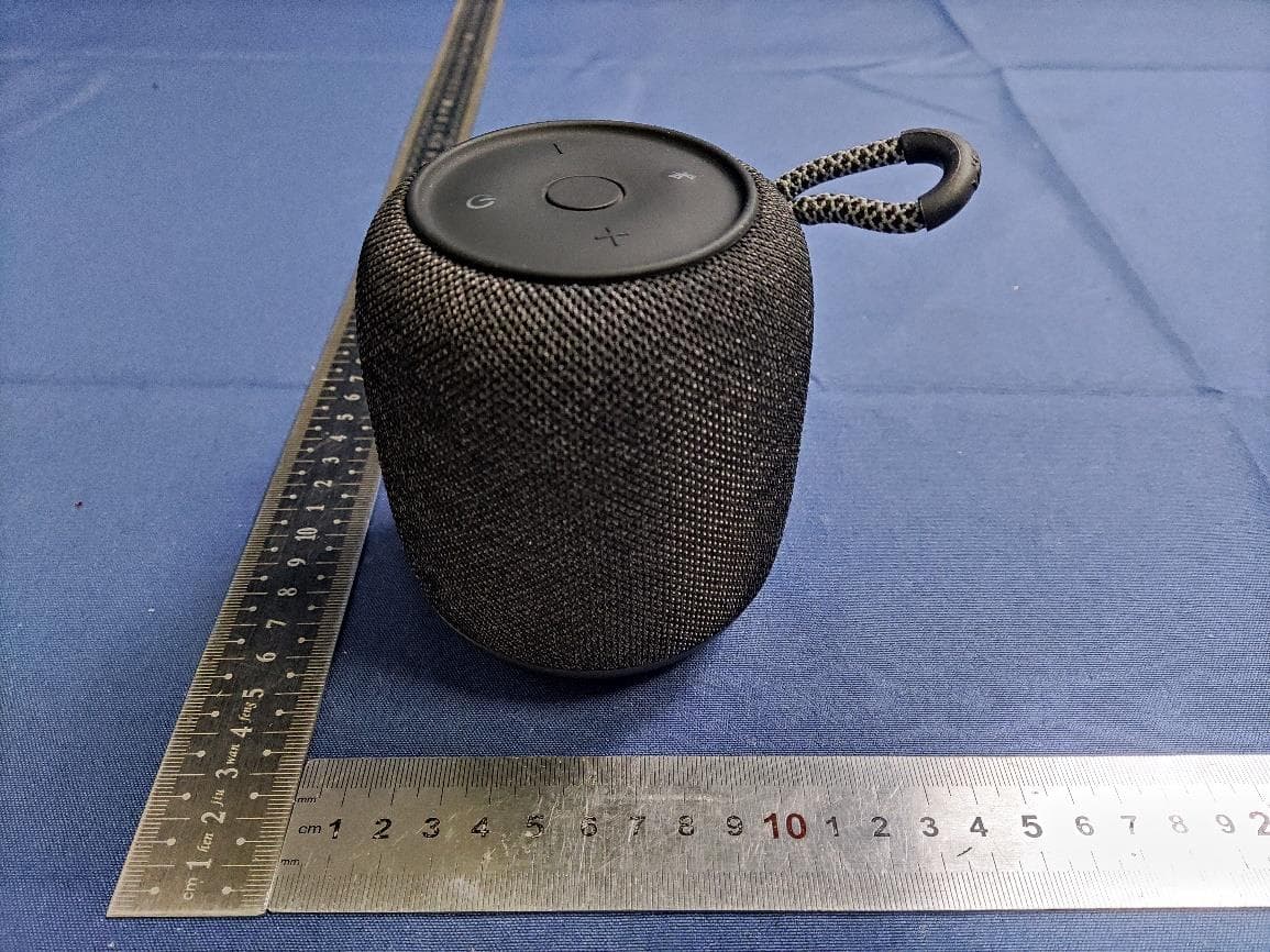
2AAP8-VIFA122
Feb 05, 2024Portable Bluetooth Speaker
Equipment Class
DSS - Part 15 Spread Spectrum Transmitter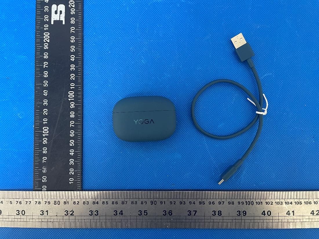
2AAP8-LT310
Jan 16, 2024Lenovo YOGA True Wireless Stereo Earbuds
Equipment Class
DTS - Digital Transmission System
2AAP8-VIFA150
Sep 27, 2023Vifa AI Intelligent Speaker
Equipment Class
DTS - Digital Transmission System
2AAP8-VIFA062
Jul 06, 2023Portable Wireless Speaker
Equipment Class
DSS - Part 15 Spread Spectrum Transmitter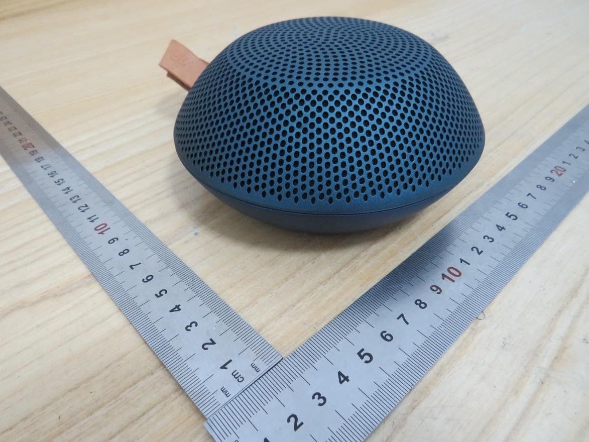
2AAP8-VIFANORDIC3-2
Jan 09, 2023Portable Wireless Speaker
Equipment Class
DSS - Part 15 Spread Spectrum Transmitter