2ABVF04011300470.25MHz transceiver
Leak Intelligence, LLC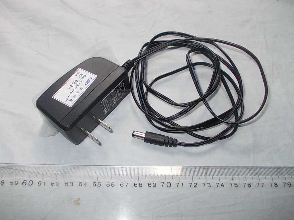
Click to zoom
Application Details
- Equipment Class
- DSR - Part 15 Remote Control/Security Device Transceiver
- Date of Grant
- Mar 17, 2014
- Application Purpose
- Original Equipment
- Date of Application
- Mar 16, 2014
- Equipment Note
- 470.25MHz transceiver
- Frequency Range
- 470.25000000 - 470.25000000
- Company
- Leak Intelligence, LLC
- Country
- United States
Documents & Files
Document Text
Text extracted from the exhibit documents filed with the FCC. Open a document above to read the original.
Users Manual
User manual 1. USE Hangzhou Lead Information Technology Co., Ltd’sC9201T-W470-LGR1,high stability, high cost performance, high lightning protection against radiation protection grade,it can be widely used in telecommunications, electric power, water conservancy, finance, transportation, energy, public security, prison, military and other different areas and different industries which need the environment and occasion of any harsh conditions for data acquisition。 2. Feature 1.Low cost, credit card size. 2.10M/100M self-adaptive cross or direct through line self-adaptive,Compatible with IEEE 802.3 protocol. 3.Capable for WEB management. 4.Device Software upgrades supporting. 5.Versatile socket operation modes: TCP Server, TCP Client, UDP,Destination IP and port can be set. 6.User’s application can communicate with device by Socket or our company software. 7.Wide Range Voltage Input. 3. Directions 1.To prevent fire or personal injury。 2.Cut off power supply when installation, on all wiring accurate rear turn it on。 3.The right way to connect or disconnect the equipment. When the equipment is under a state of electricity, please do not arbitrarily connected or disconnected cable。 4.This product is through the power cord grounding conductor. In order to prevent electric shock, the grounding conductor must be connected to the ground, you should ensure that the product is properly grounded before with this product input or output terminal connected。 5.please use the factory equipped with auxiliary parts。 6.If the cover board or panel has been unloaded, do not operate this product.。 7.when products on the electrical work, do not touch bare contact and components.。 8.If the products are damaged, please do not operate this equipment,And let it be repair by my company authorized technicians。 9.Good ventilated environment; Please do not in damp or explosive environment operation。 10.Keep surface of the equipment clean and dry。 11.Don't see the light source directly。 4. Warnning: This equipment has been tested and found to comply with the limits for a Class B digital device, pursuant to Part 15 of the FCC Rules. These limits are designed to provide reasonable protection against harmful interference in a residential installation. This equipment generates, uses, and can radiate radio frequency energy, and if not installed and used in accordance with the instructions, may cause harmful interference to radio communications. However, there is no guarantee that interference will not occur in a particular installation. If this equipment does cause harmful interference to radio or television reception, which can be determined by turning the equipment OFF and ON, the user is encouraged to try to correct the interference by one or more of the following measures: Reorient or relocate the receiving antenna Increase the separation between the equipment and receiver Connect the equipment into an outlet on a circuit different from that to which the receiver is connected Consult the dealer or an experienced radio/TV technician for help . This device complies with Part15 of the FCC Rules. Operation is subject to the following two conditions: (1) This device may not cause harmful interference, and (2) This device must accept any interference received, including interference that may cause undesired operation. The manufacturer is not responsible for any radio or TV interference caused by unauthorized modifications to this equipment. Such modifications could void the user’s authority to operate the equipment.
Block Diagram
Block Diagram FCC ID: XXX For Model: XXX
Cover Letter(s)
Leak Intelligence, LLC 501 Corporate Centre Drive Suite 310Franklin, Tennessee 37067 Tel.:(615) 496-1748 Fax: (615) 627-1971 Authority to Act as Agent Date: _02.25.2014_ American Certification Body, Inc. 6731 Whittier Avenue Suite C110 McLean, VA 22101 To Whom It May Concern: _____ AUDIX Technology (Shanghai) Co., Ltd._____ is authorized to act on our behalf, until otherwise notified, for applications to American Certification Body, Inc. (ACB). We certify that we are not subject to denial of federal benefits, that includes FCC benefits, pursuant to Section 5301 of the Anti-Drug Abuse Act of 1988, 21 U.S.C. 862. Further, no party, as defined in 47 CFR 1.2002 (b), to the application is subject to denial of federal benefits, that includes FCC benefits. Thank you, Agency Agreement Expiration Date: _____03.25.2014_____ By: __________________________ ____ Randy Ross ____ (Signature 1 ) (Print name) Title: ____ Design engineer________ On behalf of: __ Leak Intelligence, LLC _ (Company Name) Telephone: ___(615) 496-1748___ 1 - Must be signed by applicant contact given for applicant on the FCC site, or by the authorized agent if an appropriate authorized agent letter has been provided. Letters should be placed on appropriate letterhead.
External Photos
FIGURE 1 LEAK GOPHER RECEIVER (M/N: C9201T-W470-LGR1) GENERAL APPEARANCE (ALL) F IGURE 2 LEAK GOPHER RECEIVER (M/N: C9201T-W470-LGR1) GENERAL APPEARANCE (FRONT VIEW) FIGURE 3 LEAK GOPHER RECEIVER (M/N: C9201T-W470-LGR1) GENERAL APPEARANCE (BACK VIEW) F IGURE 4 LEAK GOPHER RECEIVER (M/N: C9201T-W470-LGR1) ANTENNA FIGURE 5 LEAK GOPHER RECEIVER (M/N: C9201T-W470-LGR1) PORTS F IGURE 6 LEAK GOPHER RECEIVER (M/N: C9201T-W470-LGR1) ANTENNA PORT FIGURE 15 LEAK GOPHER RECEIVER (M/N: C9201T-W470-LGR1) ADAPTOR F IGURE 16 LEAK GOPHER RECEIVER (M/N: C9201T-W470-LGR1) ADAPTOR LABEL
Internal Photos
FIGURE 7 LEAK GOPHER RECEIVER (M/N: C9201T-W470-LGR1) COVER REMOVED F IGURE 8 LEAK GOPHER RECEIVER (M/N: C9201T-W470-LGR1) MAIN BOARD (FRONT SIDE) FIGURE 9 LEAK GOPHER RECEIVER (M/N: C9201T-W470-LGR1) MAIN BOARD (BACK SIDE) F IGURE 10 LEAK GOPHER RECEIVER (M/N: C9201T-W470-LGR1) CHIP & CRYSTAL ON MAIN BOARD FIGURE 11 LEAK GOPHER RECEIVER (M/N: C9201T-W470-LGR1) RF BOARD (FRONT SIDE) F IGURE 12 LEAK GOPHER RECEIVER (M/N: C9201T-W470-LGR1) RF BOARD (BACK SIDE) FIGURE 13 LEAK GOPHER RECEIVER (M/N: C9201T-W470-LGR1) RF BOARD (SHIELDED COVER REMOVED) F IGURE 14 LEAK GOPHER RECEIVER (M/N: C9201T-W470-LGR1) CHIP & CRYSTAL ON RF BOARD
Operational Description
1 C9201T-W470-LGR1 OPERATIONAL DESCRIBTION 1 Hardware Introduction As shown in the following figures, C9201T-W470-LGR1 device servers have one Ethernet Interface port and wireless module antenna port. 2 Indicator Specification LED Name Colors Functions Status Description SYS Yellow System status Flash System working Off System booting normally ACT Green Ethernet Connection Status Flash Data transmitting Off Dis-connected DAT Green TTL COM date status Fast flash Data transmitting Slow flash Data receiving 3 Power Supply Using high-quality power adaptor, the device has a wide fluctuation tolerance and strong anti-interference and isolation quality to ensure a stable operation. Input voltage : DC5V。 Power consumption : <5W 4 Ethernet Interface Ethernet Interface: RJ45 2 10M/100M self-adaptive cross or direct through line self-adaptive Compatible with IEEE 802.3 protocol. 5 Reset RESET:Restore to default factory setting by press 3 second. 6 Wireless Module Wireless module: SRWF-1022 7 Operating Environment The device has a wide range of operating temperature and is able to work normally and stably in highly adverse environment. Working Temperature -40°C ~ +75°C Storage Temperature -40°C ~ +85°C Relative Humidity 5 %~95 % Atmospheric Pressure 70~106 kpa The environment should be free from corrosive and solvent gases, dust, and magnetic interference. 8 Mechanical Specifications Appearance dimension:78MM*60MM*30MM 9. RF Function 9.1. Features Serial number Item Parameter Note 1 Modulation mode GFSK/FSK 2 Work frequency 470.25 MHz 3 Interface velocity 4800bps 4 Power supply +3.3~5VDC 5 Working temperature -40°C~80°C 6 Working humidity 10%~90%(relative humidity without condensation) 7 Dimension 47mm×26mm×10mm 3 9.2 Transmitting Transmitting GFSK mode: JUMPER ABCD frequency 470.25MHz 9.3 Signal Description The function of the wireless module is to sent the data which is received from the RJ45 port to the air and sent the data which is received from the air to the RJ45 port. 10.Installation and Maintains 10.1.Installation STEP 1: Connect the C9201T-W470-LGR1 device server to a network. Use a standard straight -through Ethernet cable to connect to a hub or switch. When setting up or testing the C9201T-W470-LGR1 device server, you might find it convenient to connect directly to your computer’s Ethernet port. In this case, use a cross-over Ethernet cable. STEP 2: Connect the C9201T-W470-LGR1 device server’s serial port to a serial device. STEP 3: Connect the power adaptor. STEP 4: Placement options. In addition to placing the C9201T-W470-LGR1 on a desktop or other horizontal surface, you may also make use of the DIN-Rail or Wall Mount options, as illustrated below. 4 Wall Mount DIN -Rail 10.2 Method of Operation 10.2.1 Self Test Set to join the right power supply, the device will self-test, PWR light is on continuously, and all the LED digital tube displays the number 8. After self-testing, LED displays real-time voltage. 10.2.2 Set up and Connection According to the requirements of network environment is connected, open the power, equipment enter the normal working condition. If the device is not working properly, please see the fault diagnosis and exclusion, if still not rule out the possibility of failure, please contact with the company or the company dealers, agents contact.
Schematics
UART_CTS1_RXC1 UART_RTS1_TXen1 MCU UART_TXD1 UART_TXD2 UART_RXD1 UART_RXD2 UART_RTS1_TXen1 UART_CTS1_RXC1 UART_CTS2_RXC2 UART_RTS2_TXen2 M0 M1 M2 SLW POWER&&UART UART_TXD1 UART_TXD2 UART_RXD2 UART_RXD1 UART_CTS2_RXC2 UART_CTS1_RXC1 UART_RTS1_TXen1 UART_RTS2_TXen2 M0 M1 M2 SLW UART_RXD1 UART_TXD1 UART_RXD2 UART_TXD2 UART_CTS2_RXC2 M0 M1 M2 SLW UART_RTS2_TXen2 3.3V UART_RTS1_TXen1 UART_RTS2_TXen2 3.3V 3.3V R2210K LED_P2 LED_P1 RXD TXD R244.7K SS0n SMISO SMOSI 50-55 9B90酕Hibernation Module U102 LM3S9B90-C5 PA0/I2C1SCL/U0RX/U1RX 26 PA1/I2C1SDA/U0TX/U1TX 27 PA2/SSI0CLK 28 PA3/SSI0FSS 29 PA4/SSI0RX 30 PA5/SSI0TX 31 PC0/TCK/SWCLK 80 PC1/TMS/SWDIO 79 PC2/TDI 78 PC3/TDO/SWO 77 PC4/CCP1/CCP2/CCP4/CCP5 25 PC5/CO0/C1+/C10/CCP1/CCP3 24 PC6/CCP0/CCP3/U1RX 23 PC7/Clo/CCP0/CCP4/U1TX 22 PD0/CCP6/U1RX/U2RX 10 PD1/CCP2/CCP7/U1TX/U2TX 11 PD2/CCP5/CCP6/U1RX 12 PD3/CCP0/CCP7/U1TX 13 PD4 97 PD5/U2RX 98 PD6/U2TX 99 PD7 100 GND 9 GND 21 ERBIAS 33 RST 64 LDO 7 OSC0 48 OSC1 49 PB0/CCP0/U1RX 66 PB1/CCP1/CCP2/U1TX 67 PB2/CCP0/CCP3/I2C0SCL 72 PB3/I2C0SDA 65 PB4/U1RX/U2RX 92 PB5/U1TX 91 PB6 90 PB7/NMI 89 PE0/CCP3/SSI1CLK 74 PE1/CCP2/CCP6/SSI1FSS 75 PE2/SSI1RX 95 PE3/SSI1TX 96 PE4/CCP2/CCP3/U2TX 6 PA6/CCP1/I2C1SCL 34 PA7/CCP3/CCP4/I2C1SDA 35 PE6/Clo 2 PE7 1 PF0/U1DSR 47 PF1/CCP3/U1RTS 61 PF2/LED1/SSI1CLK 60 PF3/LED0/SSI1FSS 59 MDIO 58 TXON 46 TXOP 43 PF4/C0o/CCP0/SSI1RX 42 PG0/I2C1SCL/U2RX 19 PG1/I2C1SDA/U2TX 18 XTALNPHY 17 XTALPPHY 16 PF5/Clo/CCP2/SSI1TX 41 RXIP 40 RXIN 37 PG7/CCP5 36 PH0/CCP6 86 PH1/CCP7 85 PH2/Clo 84 PH3 83 AVDD 3 AGND 4 VDD33 8 VDD33 20 VDD33 32 VDD33 44 VDD33 56 VDD33 68 VDD33 81 VDD33 93 GND 45 GND 57 GND 69 GND 82 GND 94 CVDD 38 CVDD 88 HIB 51 PH4/SSI1CLK 76 USB0DP 71 USB0DM 70 USBORBIAS 73 PH5/SSI1FSS 63 PH6/SSI1RX 62 PH7/SSI1TX 15 PJ0/I2C1SCL 14 PJ1/I2C1SDA 87 PJ2/CCP0 39 WAKE 50 XOSC0 52 XOSC1 53 GND 54 VBAT 55 PE5/CCP5 5 GND SLP R39 12.4K IMP811SEUS-T U10 GND 1 RESET 2 MR 3 VCC 4 C22 0.1uF C36 22pF + C27 10uF C12 0.1uF M0 RST C34 0.1uF C37 22pF M1 C38 22pF D12LED 21 R18 100K C20 0.01uF RESET R13 10K Y11 25MHZ 21 3 C21 0.1uF M2 Y10 12MHZ 12 3 C35 22pF R3710K C24 0.1uF C32 0.1uF LEDSYS C23 0.1uF LEDLNK + C33 10uF C29 0.1uF D15LED 21 3.3V VDDC_1.2V 3.3VR285.1 RXIN2 C16 0.1uF R27 56 R30 56 R35 56 R31 56 SS0n TXON2 RESET C19 0.01uF R295.1 R335.1 C15 10pF C17 10pF R345.1 C18 10pF 3.3V C14 10pF RXIP2 TXOP2 HR901110A J12 RJ45 G1 G1 G2 G2 BO1 9 BO2 10 1 1 2 2 3 3 4 4 5 5 6 6 7 7 8 8 3.3V LED_LNK UART_CTS1_RXC1 OSC0 OSC1 CPU_RSTO D13LED 21 MCU LEDP1 U0RX D14LED 21 EB LEDP2 U0TX UART_RXD2 UB UART_TXD2 MDIO SLW SLW WP UART_RTS2_TXen2 M1 M2 M0 R25 10K J11 CON4 1 2 3 4 R10330 TXOP2 TXON2 D10 BV03C-L D11 BV03C-L RXIN2 RXIP2 PC6 SRWF-1022 R12 4.7K R11330 R15330 NC C11 0.1uF UART_CTS2_RXC2 SWCLK R16330 NC SWDIO UART_CTS2_RXC2 LED_SYS CPU_RESTORE C10 10uF SLW UART_RTS1_TXen1 LED_LNK R2310K C13 0.1uF R17 10K 3.3V S10 keypress 1 1 2 2 3.3V CPU_RESTORE LED_P1 U0TX R2010K U11W25Q80 CS 1 DO 2 WP 3 GND 4 DI 5 CLK 6 HOLD 7 VCC 8 3.3V SMOSI SMISO SCLK0 SPI flash WP U0RX UART_TXD1 UART_RXD1 UART_RXD1 UART_TXD1 LED_P2 M0 M2 M1 RP10330*4P 1 3 8 6 2 4 7 5 TXOP RXIP RXIN TXON J10 CON9 1 2 3 4 5 6 7 8 9 LED_SYS PC6 CPU_RSTO RESET R21 10K UART_CTS1_RXC1 GND UART_TXD2 UART_RXD2 UART_TXD1 SLW M0 M2 UART_TXD2 UART_RTS1_TXen1 TP1 1 3.3V R57100K TP2 1 5-28V M0 M1 M2 H50 1 R77 PTC_JK60/090__RAD0_2 D58 SMBJ6.8CA/SMBJ18CA/SMBJ28 DC05Y J51 5V 1 GND 2 GND 3 P50 CON2 12 GND M2 U51 LD1117ADJ ADJ 1 VOUT 2 VIN 3 PAD 4 3.3V R78 510 R79 820 M0 R6120 3.3V R62100K 3.3V R68100K POWER&&UART T1+ SLW H51 1 T1- T1+ 3.3V H52 1 M1 B52CBW321609U101T 12 R1- M0 3.3V T1- M1 UART_RTS2_TXen2 SLW SLW T2+ R2- T2- M2 M1 J50A 3.81_10P 1 2 3 4 5 J50B 3.81_10P 6 7 8 9 10 C53 0.1uF C55 0.1uF U50 SP336E T4IN 1 M1 2 T4O 3 T3O 4 VCC 5 T1O 6 T2O 7 GND 8 C1+ 9 V+ 10 C2+ 11 C1- 12 C2- 13 V- 14 T3I 28 T2I 27 T1I 26 SLW 25 M0 24 M2 23 R4O 22 R3O 21 R2O 20 R1O 19 R4I 18 R3I 17 R2I 16 R1I 15 D59 IN4007 R98 100K C92 0.01uF U7 MP1482/2403 EN 7 SS 8 BS 1 IN 2 SW 3 GND 4 FB 5 COMP 6 GND 0 C90 0.1uF R100 9.1K 0603 R9924K0603 L4 10uH/3A SD54 C860.1uF C0603 R101 4.7K C91 680pF/NC C89 22uF C1206 C88 10uF X5R C1812 TP3 1 R5420 R5820 R6020 TX1+ TX1- RX1+ RX1- UART_TXD1 UART_RTS1_TXen1 R1+ 3.3V 3.3V UART_CTS1_RXC1 RP51 4.7K*4P 13 86 24 75 UART_RXD1 UART_TXD1 R80 330 D52SMBJ12CA D50SMBJ12CA D51SMBJ12CA D53SMBJ12CA C54 0.1uF C51 0.1uF R5120 UART_RTS1_TXen1 D60 GREEN UART_RXD2 R50100K T2- T2+ R6620 UART_RXD1 R6920 TX2+ TX2- RX2+ RX2- R7220 R2+ D56SMBJ12CA D54SMBJ12CA D55SMBJ12CA R53100K D57SMBJ12CA R6420 3.3V 3.3V UART_CTS1_RXC1 UART_TXD2 UART_RTS2_TXen2 UART_CTS2_RXC2 UART_RXD2 UART_TXD2 UART_RTS2_TXen2 R2- R59100K R2+ R65100K C52 0.1uF R71100K R1- R1+ RP50 10K*4P 1 3 8 6 2 4 7 5 UART_CTS2_RXC2 UART_RXD2 UART_CTS1_RXC1 UART_RXD1 UART_CTS2_RXC2 杭州立地信息技术有限公司 ItemPartQuantityReference 1PCB-C902L 11 75*521PCB 3Ca pacitance-0603-10pF/50V NP0/C0G4C14,C15,C17,C18 4Ca pacitance-0603-22pF/50VC0G4C35,C36,C37,C38 5Ca pacitance-0603-0.01uF/50V X7R3C92,C19,C20 6Ca pacitance-0603-0.1uF/50V X7R13C11,C12,C13,C16,C21,C22,C23,C24,C29,C32,C34,C86, 7Capacitance-1206-10uF/16V/±20%,X5R3C10,C27,C33 8Ca pacitance-1812-10uF X5R 50V1C88 9Ca pacitance-1206-22uF/10V/±20%,X5R1C89 10Resistance-0603-5.1Ω4R28 ,R29,R33,R34 11Resistance-0603-56Ω ±5%4R27 ,R30,R31,R35 12Resistance-0603-330Ω3R10 ,R11,R80 13Resistance-0603-510Ω1R78 14Resistance-0603-820Ω1R79 15Resistance-0603-4.7KΩ3R12 ,R24,R101 16Resistance-0603-10KΩ9R13 ,R17,R20,R21,R22,R23,R25,R37,R100 17Resistance-0603-12.1K±1%1R39 18Resistance-0603-33KΩ1R99 19Resistance-0603-100KΩ1R18 20Resistance-0603-100KΩ1R98 21Resistance-330Ω*4P1RP10 22Resistance-4.7K*4P1RP51 23Chi p Bead-CBW321609U101T1B52 24LED-0805-Green1D60 25TVS-BV03C-L2D10 ,D11 26TVS-SMB J30CA1D58 27IC-SOIC8-MP24031U7 28IC-SOT-143-IMP811SEUS-T1U10 29IC-SOIC8-W25Q80BVSSIG1U11 30IC-LQFP100-LM3S9B90-IQC80-C5T1U12 31Diode-DIODE400-IN40071D59 32CON-1*91 J10 33CON-1*41 J11 34R J45-HR901110A1J12 35Power-48V-DC05Y-3P1 J51 36Cr ystal-XTAL-12MHz-49S51Y10 37Cr ystal-XTAL-25.00MHz-49S51Y11 38Vertical inductance-TLN202…
Text truncated - open the document above for the full version.
Test Report
Leak Intelligence, LLC FCC ID: 2ABVF04011300 Page 1 of 24 Audix Technology (Shanghai) Co., Ltd. Report No.: ACI-F14025 Prepared For : Leak Intelligence, LLC 501 Corporate Centre Drive Suite 310Franklin, Tennessee 37067 Prepared By : Audix Technology (Shanghai) Co., Ltd. 3 F 34 Bldg 680 Guiping Rd., Caohejing Hi-Tech Park, Shanghai 200233, China Tel : +86-21-64955500 Fax : +86-21-64955491 Report No. : ACI-F14025 Date of Test : Jan. 08 – Mar. 14, 2014 Date of Report : Mar. 15, 2014 Application for FCC Certification On behalf of Leak Intelligence, LLC Product Name: Leak Gopher Receiver Model No.: C9201T-W470-LGR1 FCC ID: 2ABVF04011300 Leak Intelligence, LLC FCC ID: 2ABVF04011300 Page 2 of 24 Audix Technology (Shanghai) Co., Ltd. Report No.: ACI-F14025 TABLE OF CONTENTS Page 1 SUMMARY OF STANDARDS AND RESULTS .......................................................................... 4 1.1 Description of Standards and Results ......................................................................................... 4 2 GENERAL INFORMATION .......................................................................................................... 5 2.1 Description of Equipment Under Test ........................................................................................ 5 2.2 Description of Test Facility ........................................................................................................ 6 2.3 Measurement Uncertainty .......................................................................................................... 6 3 CONDUCTED EMISSION TEST .................................................................................................. 7 3.1 Test Equipment ........................................................................................................................... 7 3.2 Block Diagram of Test Setup ..................................................................................................... 7 3.3 Conducted Emission Limits [FCC Part 15 Subpart C 15.207] ................................................... 7 3.4 Test Configuration ...................................................................................................................... 7 3.5 Operating Condition of EUT ...................................................................................................... 8 3.6 Test Procedures .......................................................................................................................... 8 3.7 Test Results ................................................................................................................................ 8 4 RADIATED EMISSION TEST ..................................................................................................... 10 4.1 Test Equipment ......................................................................................................................... 10 4.2 Block Diagram of Test Setup ................................................................................................... 10 4.3 Radiated Emission Limit [FCC Part 15 Subpart C 15.209] ..................................................... 11 4.4 Test Configuration .................................................................................................................... 11 4.5 Operating Condition of EUT .................................................................................................... 11 4.6 Test Procedures ........................................................................................................................ 12 4.7 Test Results .............................................................................................................................. 13 5 FUNDAMENTAL AND SPURIOUS EMISSIONS TEST ......................................................... 16 5.1 Test Equipment ......................................................................................................................... 16 5.2 Block Diagram of Test Setup ................................................................................................... 16 5.3 Fundamental and Spurious Emission Limit (FCC Part 15 Subpart C 15.231(e)) ................. 16 5.4 Test Configuration .................................................................................................................... 16 5.5 Operating Condition of EUT .................................................................................................... 17 5.6 Test Procedures ........................................................................................................................ 17 5.7 Test Results .............................................................................................................................. 18 6 BANDWIDTH MEASUREMENT ................................................................................................ 20 6.1 Test Equipment ......................................................................................................................... 20 6.2 Bandwidth Limit (FCC Part 15 Subpart C 15.231 (c)) ............................................................ 20 6.3 Test Results .............................................................................................................................. 20 7 TRANSMISSION TIME LIMIT .................................................................................................. 21 7.1 Test Equipment ......................................................................................................................... 21 7.2 Limit (FCC Part 15 Subpart C 15.231 (e)) ............................................................................... 21 7.3 Test Results .............................................................................................................................. 21 8 DEVIATION TO TEST SPECIFICATIONS ..............................................................................…
Text truncated - open the document above for the full version.
Test Setup Photos
Test Set-Up Photos 1. Conducted Emission Test 2. Radiated Electromagnetic Emission Test BELOW 1GHZ ABOVE 1GHZ L YING POSITION (WORST) S IDE POSITION S TAND POSITION
Contact Information
Applicant
Randy Ross(Design engineer)
Technical Contact
Audix Technology (Shanghai) Co., Ltd.Kwo Byron
[email protected]+86-21-64955500
3F 34Bldg 680 Guiping Rd., Caohejing Hi-Tech Park · Shanghai · China
Test Firm
Audix Technology ( Shanghai ) Co., Ltd.Byron Kwo
Technical Specifications
| # | Rule Parts | Frequency Range | Power Output |
|---|---|---|---|
| 1 | 15.231(e) | 470.25 MHz - 470.25 MHz | - |