2AFOSWT8266WT8266 Module
WIRELESS-TAG TECHNOLOGY CO., LIMITED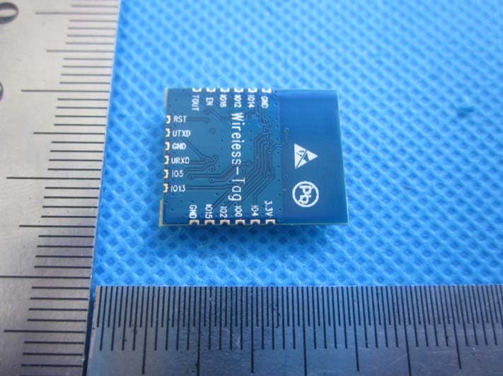
Click to zoom
Application Details
- Equipment Class
- DTS - Digital Transmission System
- Date of Grant
- Aug 31, 2015
- Application Purpose
- Original Equipment
- Date of Application
- Aug 31, 2015
- Equipment Note
- WT8266 Module
- Frequency Range
- 2412.00000000 - 2462.00000000
- Country
- China
Documents & Files
Document Text
Text extracted from the exhibit documents filed with the FCC. Open a document above to read the original.
Users Manual
OEM INTEGRATION INSTRUCTIONS: (additional information) This device is intended only for OEM integrators under the following conditions: The module must be installed in the host equipment such that 20 cm is maintained between the antenna and users, and the transmitter module may not be co-located with any other transmitter or antenna. The module shall be only used with the external antenna(s) that has been originally tested and certified with this module. As long as 3 conditions above are met, further transmitter test will not be required. However, the OEM integrator is still responsible for testing their end-product for any additional compliance requirements required with this module installed (for example, digital device emissions, PC peripheral requirements, etc.). Validity of using the module certification: In the event that these conditions cannot be met (for example certain laptop configurations or co-location with another transmitter), then the FCC authorization for this module in combination with the host equipment is no longer considered valid and the FCC ID of the module cannot be used on the final product. In these circumstances, the OEM integrator will be responsible for re-evaluating the end product (including the transmitter) and obtaining a separate FCC authorization. Information that must be placed in the end user manual: The OEM integrator has to be aware not to provide information to the end user regarding how to install or remove this RF module in the user's manual of the end product which integrates this module. The end user manual shall include all required regulatory information/warning as show in this manual. This host device must be kept away from all persons by 20cm or more and installations using less distance, or installations using antennas with gain greater than that with which this was Certified will require additional approvals.
Users Manual
ESP8266EX Datasheet Version 4.3 Espressif Systems IOT Team http://bbs.espressif.com/ Copyright © 2015 Disclaimer and Copyright Notice Information in this document, including URL references, is subject to change without notice. THIS DOCUMENT IS PROVIDED "AS IS" WITH NO WARRANTIES WHATSOEVER, INCLUDING ANY WARRANTY OF MERCHANTABILITY, NON-INFRINGEMENT, FITNESS FOR ANY PARTICULAR PURPOSE, OR ANY WARRANTY OTHERWISE ARISING OUT OF ANY PROPOSAL, SPECIFICATION OR SAMPLE. All liability, including liability for infringement of any proprietary rights, relating to use of information in this document is disclaimed. No licenses express or implied, by estoppel or otherwise, to any intellectual property rights are granted herein. The Wi-Fi Alliance Member Logo is a trademark of the WiFi Alliance. All trade names, trademarks and registered trademarks mentioned in this document are property of their respective owners, and are hereby acknowledged. Copyright © 2015 Espressif Systems. All rights reserved. 1.General Overview 6 .................................................................................................. 1.1.Introduction 6 ............................................................................................................. 1.2.Features 7 .................................................................................................................... 1.3.Parameters 7 ............................................................................................................... 1.4.Ultra Low Power Technology 9 ................................................................................. 1.5.Major Applications 9 .................................................................................................. 2.Hardware Overview 11 ............................................................................................. 2.1.Pin Definitions 11 ......................................................................................................... 2.2.Electrical Characteristics 13 ........................................................................................ 2.3.Power Consumption 13 ............................................................................................. 2.4.Receiver Sensitivity 14 ............................................................................................... 2.5.MCU 15 ........................................................................................................................ 2.6.Memory Organization 15 .......................................................................................... 2.6.1. Internal SRAM and ROM 15 ...................................................................................... 2.6.2. External SPI Flash 15 .................................................................................................. 2.7.AHB and AHB Blocks 16 ............................................................................................ 3.Pins and Definitions 17 ............................................................................................. 3.1.GPIO 17 ....................................................................................................................... 3.1.1. General Purpose Input/Output Interface (GPIO) 17 ............................................. Table of Contents 3.2.Secure Digital Input/Output Interface (SDIO) 18 .................................................. 3.3.Serial Peripheral Interface (SPI/HSPI) 18 ................................................................. 3.3.1. General SPI (Master/Slave) 18 ................................................................................. 3.3.2. SDIO / SPI (Slave) 19 ................................................................................................. 3.3.3. HSPI (Master/Slave) 19 ............................................................................................. 3.4.Inter-integrated Circuit Interface (I2C) 19 ............................................................... 3.5.I2S 20 ........................................................................................................................... 3.6.Universal Asynchronous Receiver Transmitter (UART) 20 ..................................... 3.7.Pulse-Width Modulation (PWM) 21 ......................................................................... 3.8.IR Remote Control 22 ................................................................................................ 3.9.ADC (Analog-to-digital Converter) 22 .................................................................... 3.10.LED Light and Button 24 ........................................................................................... 4.Firmware & Software Development Kit 26 ............................................................ 4.1.Features 26 .................................................................................................................. 5.Power Management 27 ............................................................................................ 6.Clock Management 28 ............................................................................................. 6.1.High Frequency Clock 28 .......................................................................................... 6.2.External Reference Requirements 29 ...................................................................... 7.Radio 29 ...................................................................................................................... 7.1.Channel Frequencies 30 ........................................................................................... 7.2.2.4 GHz Receiver 30 .................................................................................................. 7.3.2.4 GHz Transmitter 30 .............................................................................................. 7.4.Clock Generator 30 .................................................…
Text truncated - open the document above for the full version.
Cover Letter(s)
WIRELESS-TAG TECHNOLOGY CO., LIMITED FCC Authorization Letter Number: CF304 Version: V03 Date: 01-08-2011 We, (the approval holder) Company name WIRELESS-TAG TECHNOLOGY CO., LIMITED Address 4/F., BAK Sci & Tech Building, No. 9 Keyan Road, Science & Technology Park Central, City Nanshan District, Shenzhen, Country China(Post Code:518057) declare that the following representative (agent): Name (person) [email protected] Company name Shenzhen BCTC Technology Co., Ltd. Address No.101,Yousong Road,Longhua New District, City Shenzhen Country China is hereby authorized to apply the following equipment for certification on our behalf: Product Description WT8266 Type or Model(s) WT8266 Tradename or Brand(s) N/A We also authorize Teleconformity (Mr. M. Koop, Manager Certification, Address: Rietven 31, 7534NH Enschede, the Netherlands) to apply and sign this application for certification, registration or filing on our behalf (as representative agent or certifier). Attestation: City and Country: Date: Name: (this must be a person) Function:Signature: (or official company stamp) Nanshan District, Shenzhen, 2015-8-22 Ming Li Manager
Cover Letter(s)
WIRELESS-TAG TECHNOLOGY CO., LIMITED FCC Confidentiality Request Number: CF303 Version: V05 Date: 21-05-2012 (Permanent or also called long term confidentiality is the normal method to keep certain docuements confidential, and may apply to schematics, block diagrams, operational description and bill of materials.) To: Federal Communications Commission Equipment Authorization Branch 7435 Oakland Mills Road Columbia, MD 21046 Pursuant to 47 CFR Section 0.459(a) & (b), we, (the applicant / grantee) Company name WIRELESS-TAG TECHNOLOGY CO., LIMITED Address 4/F., BAK Sci & Tech Building, No. 9 Keyan Road, Science & Technology Park Central, City Nanshan District, Shenzhen, Country China(Post Code:518057) request for this certification filing under: Grantee Code Product Number FCC ID: 2AFOS WT8266 to maintain permanent confidentiality for the following documents submitted within this application: (please cross what is applicable, or add other documents, provide the file name and description) Exhibit File Name Description x Operational Description explaining the functioning of the block diagram x Block Diagrams showing the systematic building blocks of the EUT x Schematics Diagrams showing components, their values and interconnection Above materials crossed contain secrets, proprietary and technical information, which would customarily be guarded from competitors under 47 CFR, section 0.457(d)(2). Disclosure or publication or any portion of this company confidential material to other parties could cause substantial competitive harm and provide unjustified benefits for competitors. We understand that pursuant to 47 CFR section 0.457(d)(1)(ii) disclosure of the applicant and all accompanying documentation will not be made before the date of the grant. The documents indicated as confidential above, are not publicly available elsewhere. Attestation: City and Country: Date: Name: (this must be a person) Function:Signature: (or official company stamp) Nanshan District, Shenzhen, 2015-8-22 Ming Li Manager
Cover Letter(s)
WIRELESS-TAG TECHNOLOGY CO., LIMITED FCC Modular Approval Request Number:CF305 Version: V03 Date: 01-08-2011 To the FCC or FCC TCB handling this application Hereby we, Company name (grantee) WIRELESS-TAG TECHNOLOGY CO., LIMITED Addresss 4/F., BAK Sci & Tech Building, No. 9 Keyan Road, Science & Technology Park Central, City / ZIP / State / Country Nanshan District, Shenzhen,/China request modular approval for the certification of our equipment within this application, identified by: FCC ID: 2AFOSWT8266 The table below contains the justification for modular approval of this equipment: Requirement per DA 00-1407 Explanation from grantee (do not write yes / no, but explain why it complies / how it is achieved) 1. The modular transmitter must have its own RF shielding. YES,the modular transmitter have its own RF shielding. 2. The modular transmitter must have buffered modulation/data inputs (if such inputs are provided) to ensure that the module will comply with Part 15 requirements under conditions of excessive data rates or over-modulation. YES, the modular transmitter have buffered modulation data inputs. 3. The modular transmitter must have its own power supply regulation. YES, the modular have its own power supply 4. The modular transmitter must comply with the antenna requirements of Section 15.203 and 15.204(c). The antenna must either be permanently attached or employ a “unique” antenna coupler (at all connections between the module and the antenna, including the cable).. YES, the modular transmitter 5. The modular transmitter must be tested in a stand-alone configuration, i.e., the module must not be inside another device during testing. This is intended to demonstrate that the module is capable of complying with Part 15 emission limits regardless of the device into which it is eventually installed. YES, The modular can be tested in a stand-alone configuration. 6. The modular transmitter must be labeled with its own FCC ID number, and, if the FCC ID is not visible when the module is installed inside another device, then the outside of the device into which the module is installed must also display a label referring to the enclosed module. This exterior label can use wording such as the following: “Contains Transmitter Module FCC ID: XYZMODEL1” or “Contains FCC ID: XYZMODEL1.” Any similar wording that expresses the same meaning may be used. The Grantee may either provide such a label, an example of which must be included in the application for equipment authorization, or, must provide adequate instructions along with the module which explain this requirement. In the latter case, a copy of these instructions must be included in the application for equipment authorization. YES, the ID number on the shielding cover. 7. The modular transmitter must comply with any specific rule or operating requirements applicable to the transmitter and the manufacturer must provide adequate instructions along with the module to explain any such requirements. A copy of these instructions must be included in the application for equipment authorization. For example, there are very strict operational and timing requirements that must be met before a transmitter is authorized for operation under Section 15.231. For instance, data transmission is prohibited, except for operation under Section 15.231(e), in which case there are separate field strength level and timing requirements. Compliance with these requirements must be assured. YES, the some operating requirements on manual. 8. The modular transmitter must comply with any applicable RF exposure requirements. For example, FCC Rules in Sections 2.1091, 2.1093 and specific Sections of Part 15, including 15.319(i), 15.407(f), 15.253(f) and 15.255(g), require that Unlicensed PCS, UNII and millimeter wave devices perform routine environmental evaluation for RF Exposure to demonstrate compliance. In addition, spread spectrum transmitters operating under Section 15.247 are required to address RF Exposure compliance in accordance with Section 15.247(b)(4). Modular transmitters approved under other Sections of Part 15, when necessary, may also need to address certain RF Exposure concerns, typically by providing specific installation and operating instructions for users, installers and other interested parties to ensure compliance. YES, the modular transmitter comply with a applicable RF exposure requirements. Attestation (by grantee) City and Country: Date: Name: (this must be a person) Function: Signature: (or official company stamp) Nanshan District, Shenzhen, 2015-8-22 Ming Li Manager
ID Label/Location Info
M/N: WT8266 FCC ID: 2AFOSWT8266 Label location
Internal Photos
Antenna location
RF Exposure Info
FCC §15.247 (i), §2.1091 – RF Exposure FCC ID: 2AFOSWT8266 Applied procedures / limit According to FCC §15.247(i) and §1.1307(b)(1), systems operating under the provisions of this section shall be operated in a manner that ensures that the public is not exposed to radio frequency energy level in excess of the Commission’s guidelines. Limits for Occupational / Controlled Exposure Frequency Range (MHz) Electric Field Strength (E) (V/m) Magnetic Field Strength (H) (A/m) Power Density (S) (mW/ cm 2 ) Averaging Time |E| 2 ,|H| 2 or S (minutes) 0.3-3.0 614 1.63 (100)* 6 3.0-30 1842 / f 4.89 / f (900 / f)* 6 30-300 61.4 0.163 1.0 6 300-1500 F/300 6 1500-100,000 5 6 Note: ƒ is frequency in MHz * = Power density limit is applicable at frequencies greater than 100 MHz Limits for General Population / Uncontrolled Exposure Frequency Range (MHz) Electric Field Strength (E) (V/m) Magnetic Field Strength (H) (A/m) Power Density (S) (mW/ cm 2 ) Averaging Time |E| 2 ,|H| 2 or S (minutes) 0.3-1.34 614 1.63 (100)* 30 1.34-30 824/f 2.19/f (180/f)* 30 30-300 27.5 0.073 0.2 30 300-1500 F/1500 30 1500-100,000 1.0 30 Note: f = frequency in MHz * = Plane-wave equivalent power density MPE PREDICTION Predication of MPE limit at a given distance, Equation from OET Bulletin 65, Edition 97-01 Where: S = power density P = power input to antenna G = power gain of the antenna in the direction of interest relative to an isotropic radiator R = distance to the center of radiation of the antenna TEST RESULTS Maximum peak output power (dBm) Output power to antenna (mW) Antenna Gain (numeric) Power Density (S) (mW/ cm2) Limit of Power Density (S) (mW/ cm2) Result 20 100 1.00(0.0dBi) 0.01989 1 Pass
Test Report
FCC Part 15C Test Report FCC ID: 2AFOSWT8266 Product Name: WT8266 Trademark: N/A Model Name : WT8266 Prepared For : WIRELESS-TAG TECHNOLOGY CO., LIMITED Address : 4/F., BAK Sci & Tech Building, No. 9 Keyan Road, Science & Technology Park Central, Nanshan District, Shenzhen, China(Post Code:518057) Prepared By : Shenzhen BCTC Technology Co., Ltd. Address : No.101,Yousong Road,Longhua New District, Shenzhen,China Test Date: Aug. 8 - Aug. 18, 2015 Date of Report : Aug. 19, 2015 Report No.: BCTC-15080200 TEST RESULT CERTIFICATION Applicant’s name ................. : WIRELESS-TAG TECHNOLOGY CO., LIMITED Address ................................. : 4/F., BAK Sci & Tech Building, No. 9 Keyan Road, Science & Technology Park Central, Nanshan District, Shenzhen, China(Post Code:518057) Manufacture's Name ............ : WIRELESS-TAG TECHNOLOGY CO., LIMITED Address ................................. : 4/F., BAK Sci & Tech Building, No. 9 Keyan Road, Science & Technology Park Central, Nanshan District, Shenzhen, China(Post Code:518057) Product description Product name ........................... : WT8266 Model and/or type reference : WT8266 Serial Model .............................. : N/A Standards ............................. : FCC Part15.247 Test procedure .............................. ANSI C63.10-2013 This device described above has been tested by BCTC, and the test results show that the equipment under test (EUT) is in compliance with the FCC requirements. And it is applicable only to the tested sample identified in the report. This report shall not be reproduced except in full, without the written approval of BCTC, this document may be altered or revised by BCTC, personal only, and shall be noted in the revision of the document. Testing Engineer : (Eric Yang) Technical Manager : (Sophia Lee) Authorized Signatory : (Casey Wang) Table of Contents Page 1 . SUMMARY OF TEST RESULTS 5 1.1 TEST FACILITY 5 1.2 MEASUREMENT UNCERTAINTY 5 2 . GENERAL INFORMATION 6 2.1 GENERAL DESCRIPTION OF EUT 6 2.2 DESCRIPTION OF TEST MODES 7 2.3 BLOCK DIGRAM SHOWING THE CONFIGURATION OF SYSTEM TESTED 8 2.4 DESCRIPTION OF SUPPORT UNITS(CONDUCTED MODE) 8 2.5 EQUIPMENTS LIST FOR ALL TEST ITEMS 9 3 . EMC EMISSION TEST 10 3.1 CONDUCTED EMISSION MEASUREMENT 10 3.1.1 POWER LINE CONDUCTED EMISSION LIMITS 10 3.1.2 TEST PROCEDURE 10 3.1.3 DEVIATION FROM TEST STANDARD 10 3.1.4 TEST SETUP 11 3.1.5 EUT OPERATING CONDITIONS 11 3.1.6 TEST RESULTS 11 3.2 RADIATED EMISSION MEASUREMENT 12 3.2.1 RADIATED EMISSION LIMITS 12 3.2.2 TEST PROCEDURE 12 3.2.3 DEVIATION FROM TEST STANDARD 13 3.2.4 TEST SETUP 13 3.2.5 EUT OPERATING CONDITIONS 14 3.2.6 TEST RESULTS (BETWEEN 9KHZ – 30 MHZ) 15 3.2.7 TEST RESULTS (BETWEEN 30MHZ – 1GHZ) 16 3.2.8 TEST RESULTS (ABOVE 1000 MHZ) 18 4 . POWER SPECTRAL DENSITY TEST 23 4.1 APPLIED PROCEDURES / LIMIT 23 4.1.1 TEST PROCEDURE 23 4.1.2 DEVIATION FROM STANDARD 23 4.1.3 TEST SETUP 23 4.1.4 EUT OPERATION CONDITIONS 23 4.1.5 TEST RESULTS 24 5 . BANDWIDTH TEST 30 5.1 APPLIED PROCEDURES / LIMIT 30 5.1.1 TEST PROCEDURE 30 5.1.2 DEVIATION FROM STANDARD 30 5.1.3 TEST SETUP 30 5.1.4 EUT OPERATION CONDITIONS 30 Table of Contents Page 5.1.5 TEST RESULTS 31 6 . PEAK OUTPUT POWER TEST 37 6.1 APPLIED PROCEDURES / LIMIT 37 6.1.1 TEST PROCEDURE 37 6.1.2 DEVIATION FROM STANDARD 37 6.1.3 TEST SETUP 37 6.1.4 EUT OPERATION CONDITIONS 37 6.1.5 TEST RESULTS 38 7 . 100 KHZ BANDWIDTH OF FREQUENCY BAND EDGE 39 7.1 DEVIATION FROM STANDARD 39 7.2 TEST SETUP 39 7.3 EUT OPERATION CONDITIONS 40 7.4 TEST RESULTS 40 8 . ANTENNA REQUIREMENT 45 8.1 STANDARD REQUIREMENT 45 8.2 EUT ANTENNA 45 9 . EUT TEST PHOTO 46 10 . PHOTO OF THE EUT 47 1. SUMMARY OF TEST RESULTS Test procedures according to the technical standards: FCC Part15 (15.247) , Subpart C Standard Section Test Item Judgment Remark 15.207 Conducted Emission N/A 15.247 (a)(2) 6dB Bandwidth PASS 15.247 (b) Peak Output Power PASS 15.247 (c) Radiated Spurious Emission PASS 15.247 (d) Power Spectral Density PASS 15.205 Band Edge Emission PASS 15.203 Antenna Requirement PASS NOTE: (1)” N/A” denotes test is not applicable in this Test Report Test produce reference KDB558074 D01 DTS Meas Guidance v03r03 1.1 TEST FACILITY Shenzhen BCTC Technology Co., Ltd. Add. : No.101,Yousong Road,Longhua New District, Shenzhen,China FCC Registered No.: 187086 1.2 MEASUREMENT UNCERTAINTY The reported uncertainty of measurement y ± U,where expended uncertainty U is based on a standard uncertainty multiplied by a coverage factor of k=2,providing a level of confidence of approximately 95 %。 No. Item Uncertainty 1 Conducted Emission Test ±1.38dB 2 RF power,conducted ±0.16dB 3 Spurious emissions,conducted ±0.21dB 4 All emissions,radiated(<1G) ±4.68dB 5 All emissions,radiated(>1G) ±4.89dB 6 Temperature ±0.5°C 7 Humidity ±2% 2. GENERAL INFORMATION 2.1 GENERAL DESCRIPTION OF EUT Equipment WT8266 Trade Name N/A Model Name WT8266 Serial Model N/A Model Difference All the model are the same circuit and RF module,except model names. Product Description The EUT is a WT8266 Operation Frequency: 802.11b/g/n20MHz:2412~2462 MHz Modulation Type: OFDM/DSSS Bit Rate of Transmitter 802.11b:11/5.5/2/1 Mbps 802.11g:54/48/36/24/18/12/9/6Mbps 802.11n Up to 72Mbps Number Of Channel 11 CH, Please see Note 2. Antenna Designation: Please see Note 3. Antenna Gain (dBi) 0.0dbi Based on the application, features, or specification exhibited in User's Manual, the EUT is considered as an ITE/Computing Device. More details of EUT technical specification, please refer to the User's Manual. Channel List Please refer to the Note 2. Adapter N/A Battery N/A Connecting I/O Port(s) Please refer to the User's Manual Note: 1. For a more detailed features description, please refer to the manufacturer’s specifications or the User's Manual. 2. Channel List for 802.11b/g/n(20) Channel Frequency (MHz) Channel Frequency (MHz) Channel Frequency (MHz) Channel Frequency (MHz) 01 2412 04 2427 07 2442 10 2457 02 2417 05 2432 08 2447 11 2462 03 2422 06 2437 09 2452 3.…
Text truncated - open the document above for the full version.
Test Setup Photos
Radiated Measurement Photos
Contact Information
Applicant
Louie Wang(Manager)
Technical Contact
Test Firm
Shenzhen BCTC Technology Co., Ltd.James Zhang
Technical Specifications
| # | Rule Parts | Frequency Range | Power Output |
|---|---|---|---|
| 1 | 15C | 2.41 GHz - 2.46 GHz | 76.60 mW |
Other Applications from WIRELESS-TAG TECHNOLOGY CO., LIMITED
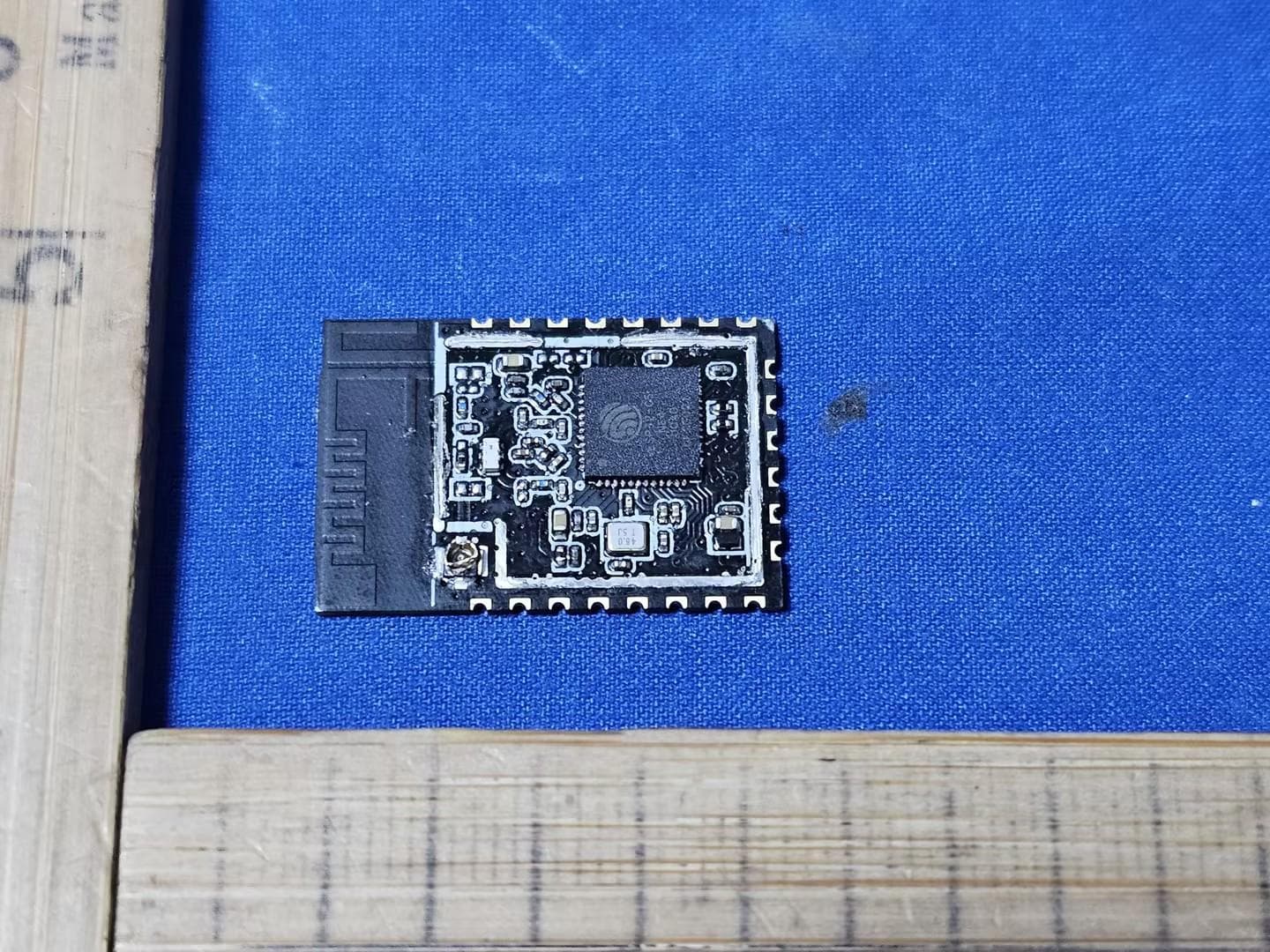
2AFOS-WT0132C5-S5
Mar 11, 2026WiFi + BLE Module
Equipment Class
NII - Unlicensed National Information Infrastructure TX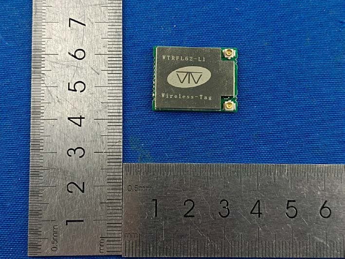
2AFOS-WTLRC262-SG3
Jul 30, 2024WIFI/BLE/lora Module
Equipment Class
DTS - Digital Transmission System2AFOS-WT8089-SF1
Mar 30, 2023WIFI Module
Equipment Class
DTS - Digital Transmission System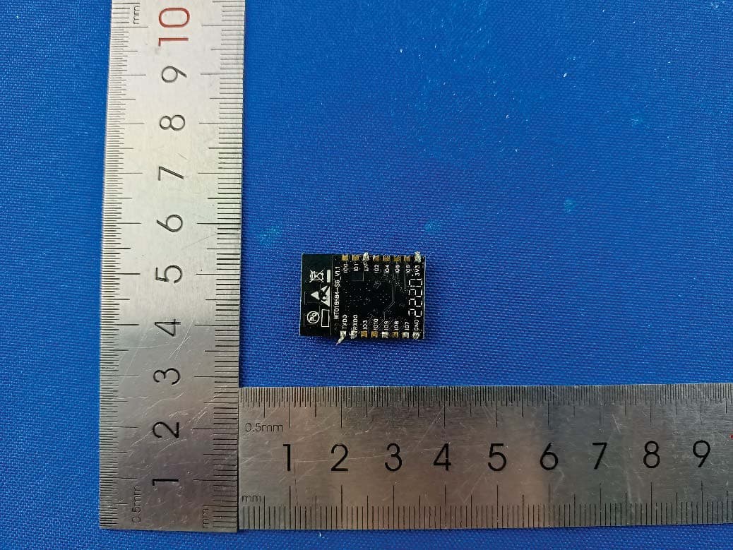
2AFOS-WT018684-S5
Jan 16, 2023WIFI BLE Module
Equipment Class
DTS - Digital Transmission System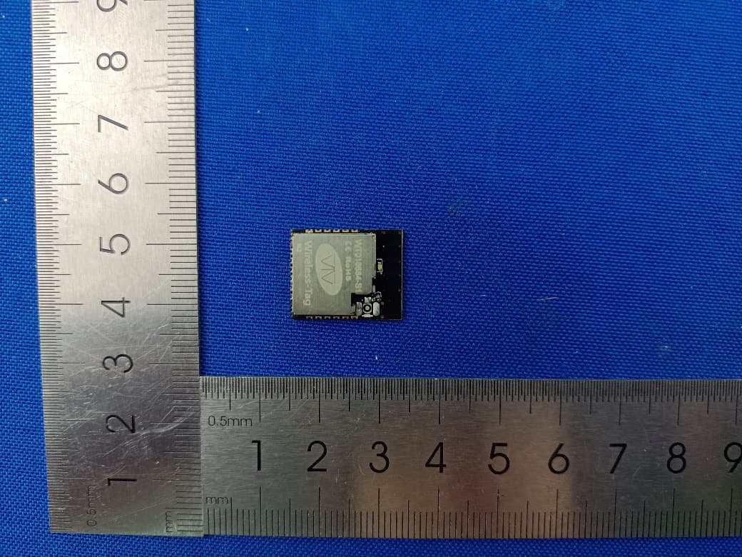
2AFOS-WT018684-S1
Jan 16, 2023WIFI BLE Module
Equipment Class
DTS - Digital Transmission System