2AFZZPCC4GMobile Phone
Xiaomi Communications Co., Ltd.Application Details
- Equipment Class
- CBE - Citizens Band End User Devices
- Date of Grant
- Sep 03, 2024
- Application Purpose
- Original Equipment
- Date of Application
- Sep 02, 2024
- Equipment Note
- Mobile Phone
- Frequency Range
- 3600.00000000 - 3649.98000000
- Country
- China
Documents & Files
Document Text
Text extracted from the exhibit documents filed with the FCC. Open a document above to read the original.
Cover Letter(s)
Rev. 1/1/03 Xiaomi Communications Co., Ltd. #019, 9th Floor, Building 6, 33 Xi'erqi Middle Road, Haidian District,Beijing,China10085 Tel: 010 6060 6666 Date: August 21, 2024 Federal Communications Commission Authorization and Evaluation Division Confidentiality Request regarding application for certification of FCC ID: 2AFZZPCC4G Pursuant to Sections 0.457 and 0.459 of the Commission’s Rules, we hereby request confidential treatment of information accompanying this application as outlined below: Schematics Block Diagram Parts List Operation Description Tune Up Procedure Software operational description The above materials contain trade secrets and proprietary information not customarily released to the public. The public disclosure of these materials may be harmful to the applicant and provide unjustified benefits to its competitors. The applicant understands that pursuant to Section 0.457 of the Rules, disclosure of this application and all accompanying documentation will not be made before the date of the Grant for this application. Sincerely, _______________ Contact Person: qingyaozeng E-mail: [email protected]
Cover Letter(s)
Xiaomi Communications Co., Ltd. #019, 9th Floor, Building 6, 33 Xi'erqi Middle Road, Haidian District,Beijing,China10085 Tel: 010 6060 6666 Date: August 21, 2024 Power of Attorney To whom it may concern, Please be notified that I, qingyaozeng, have designated Joey Lao in BV 7Layers Communications Technology (Shenzhen) Co.,Ltd as the person being responsible for this project and to sign the form 731 and other documentation. Any and all acts carried out by Joey Lao in BV 7Layers Communications Technology (Shenzhen) Co.,Ltd on the matters of relating to all processes required in the FCC approval and any communication needed with the national authority, shall have the same legal authority as acts on our own behalf. We further certifies that neither the applicant nor any party to this application, as defined in 47 CFR Ch. 1.2002 (b), is subject to a denial to Federal benefits, that include FCC benefits, pursuant to section 5301 of the Anti-Drug Abuse Act of 1998, 21 U.S.C 862. This authorization is limited to the product of as following: FCC ID: 2AFZZPCC4G If you have any acknowledgement and response, please send it to BV 7Layers Communications Technology (Shenzhen) Co.,Ltd directly. Should you have any questions or comments regarding this matter, please have my best attention. Sincerely yours, ____ Contact Person: qingyaozeng E-mail: [email protected]
Cover Letter(s)
1/1 Xiaomi Communications Co., Ltd. #019, 9th Floor, Building 6, 33 Xi'erqi Middle Road, Haidian District,Beijing,China10085 Tel: 010 6060 6666 Date: August 21, 2024 Federal Communications Commission Authorization and Evaluation Division RE : Certification Application FCC ID : 2AFZZPCC4G To Whom It May Concern, Pursuant to sections 0.457 and 0.459 of CFR 47, Public Notice DA 04-1705 of the Commission’s policy and to avoid premature release of sensitive information prior to marketing or release of the product to the public, the applicant requests the following documents contained in this certification application be temporarily withheld from public disclosure for an initial period of 180 days: ⚫ External Photos ⚫ Internal Photos ⚫ Test set-up photos ⚫ Users Manual The application contains technical information, which Xiaomi Communications Co., Ltd. deems to be trade secrets and proprietary. If made public, the information might be used to the disadvantage of the applicant in the market place. The Applicant understands that pursuant to Rule 0.457, disclosure of this Application and all accompanying documentation will not be made before the date of the Grant for this application Sincerely, ____ Contact Person: qingyaozeng E-mail: [email protected]
Cover Letter(s)
Data referencing for different Skus Template Test Data Referencing Justification of Test Data Referencing, for EMC/RF and SAR Reference model: FCC ID: 2AFZZRAD4G for the O17 Redmi. Variant model: FCC ID: 2AFZZPCC4G for the O17P POCO. Revision: Version Description Date 1.0 Initial release 2024/6/18 Contents ⚫ Product Overview ⚫ Antenna Diagram ⚫ Comparison – Summary ⚫ Exterior View ⚫ Main board Schematic ⚫ Block Diagram ⚫ BOM ⚫ PCB Layout ⚫ Test Strategy ⚫ Product Overview Radio Frequency band FCC Rule Part FCC ID: 2AFZZRAD4G (O17) FCC ID: 2AFZZPCC4G (O17P) GSM 850,900,1800,1900 Part 22, 24 Supported Supported WCDMA 1,2,4,5,6,8,19 Part 22, 24, 27 Supported Supported LTE Band 1, 2, 3, 4, 5, 7, 8, 12, 13, 17, 18, 19, 20, 26, 28, 32, 38, 40, 41, 42,48, 66 Part 22, 24, 27, 90, 96 Supported Supported 5G NR n1, n2, n3, n5, n7, n8, n12, n20, n26, n28, n38, n40, n41, n48, n66, n77, n78 Part 22, 24, 27, 90, 96 Supported Supported Wi-Fi 2.4GHz: 2.400 – 2.4845GHz 5GHz: 5.15 – 5.35GHz, 5.47 – 5.725GHz, 5.725 – 5.85GHz Part 15C&E Supported Supported Bluetooth BR&EDR &BLE 2.4GHz:2.400 – 2.4835GHz Part 15C Supported Supported NFC 13.56MHz Part 15C Supported Supported ⚫ Antenna Diagram The Antenna diagram of the FCC ID: 2AFZZPCC4G (Variant model) is same as the FCC ID: 2AFZZRAD4G (Reference model). FCC ID: 2AFZZRAD4G (O17 redmi as the Reference Model) FCC ID:2AFZZPCC4G (O17P POCO as the Variant model) Please refer to Appendix A Note2 for details Antenna No. Redmi Global FCC ID: 2AFZZRAD4G POCO Global FCC ID:2AFZZPCC4G Antenna 1 GSM-TRX: 2/3/5/8 WCDMA-TRX: 1/2/4/5/8/6/19 LTE-TRX: 1/2/3/4/5/7/8/12/13/17/18/19/20/26/28/38/40/ 41/66 NR-TRX:1/3/4/5/7/8/20/28/38/40/41/66 SRS:n41 GSM-TRX: 2/3/5/8 WCDMA-TRX: 1/2/4/5/8/6/19 LTE-TRX: 1/2/3/4/5/7/8/12/13/17/18/19/20/26/28/38/40/ 41/66 NR-TRX:1/3/4/5/7/8/20/28/38/40/41/66 SRS:n41 Antenna 2 NR-DM: n77/78/ N48/B42/B48 SRS: n77/78 NR-DM: n77/78/ N48/B42/B48 SRS: n77/78 Antenna 3 LTE-TRX: 1/3/4/7/20/32/38/40/41/66 LTE/NR-PM: 1/3/4/7/38/40/41/66/77/78/N48/B42/B48 SRS: n41/77/78 LTE-TRX: 1/3/4/7/20/32/38/40/41/66 LTE/NR-PM: 1/3/4/7/38/40/41/66/77/78/N48/B42/B48 SRS: n41/77/78 Antenna 4 GSM-DRX: 2/3/5/8 WCDMA-DRX: 1/2/4/5/8/6/19 LTE-DRX: 1/2/3/4/5/7/8/12/13/17/18/19/20/26/28/38/40/ 41/66 NR-DRX:1/3/4/5/7/8/20/28/38/40/41/66 SRS:n41 GSM-DRX: 2/3/5/8 WCDMA-DRX: 1/2/4/5/8/6/19 LTE-DRX: 1/2/3/4/5/7/8/12/13/17/18/19/20/26/28/38/40/ 41/66 NR-DRX:1/3/4/5/7/8/20/28/38/40/41/66 SRS:n41 Antenna 5 NR-TRX: n77/78/N48/B42/B48 SRS: n77/78 NR-TRX: n77/78/N48/B42/B48 SRS: n77/78 Antenna 6 GPS /2.4G/5G GPS /2.4G/5G Antenna 7 LTE-DRX: 32 NR-DRX: 77/78/ N48/B42/B48 LTE/NR-DM: 1/3/4/7/38/40/41/66 LTE-DRX: 32 NR-DRX: 77/78/48/B42/B48 LTE/NR-DM: 1/3/4/7/38/40/41/66 SRS: n41/77/78 SRS: n41/77/78 NFC The NFC antenna between FCC ID: 2AFZZRAD4G and FCC ID:2AFZZPCC4G is same, including pattern/circuit/gain/shape The NFC antenna between FCC ID: 2AFZZRAD4G and FCC ID:2AFZZPCC4G is same, including pattern/circuit/gain/shape Comments N/A ⚫ Comparison – Summary The hardware/software of the FCC ID: 2AFZZPCC4G (Variant model) is same as the FCC ID: 2AFZZRAD4G (Reference model) except for marketing name, please refer to the following for more details: 1. Identical • Supports same RF bands; • The antenna/hardware and components of the Cellular WLAN/BT/GNSS module; • The size of dimensions/display area and housing material are identical; 2. Difference: • The NFC antenna and marketing name, and the camera are difference. ⚫ Main board Schematic The Main board Schematic of the FCC ID: 2AFZZPCC4G (Variant model) is same as the FCC ID: 2AFZZRAD4G (Reference model) except for components on PCB (board ID). ⚫ Block Diagram The Block diagram of the FCC ID: 2AFZZPCC4G (Variant model) is same as the FCC ID: 2AFZZRAD4G (Reference model) without any differences. ⚫ BOM The Bomlist of the FCC ID: 2AFZZPCC4G (Variant model) is same as the FCC ID: 2AFZZRAD4G (Reference model) except for and camera, please refer to the following for more details: Please refer to Appendix A Note 6 for details Board ID: Please refer to Appendix A Note 4 for details The Redmi Global version has three cameras, while the POCO Global version has only two cameras. The POCO version does not have the following materials. Please refer to Appendix A Note 5 for details ⚫ PCB Layout: The PCB layout of the FCC ID: 2AFZZPCC4G (Variant model) is same as the FCC ID: 2AFZZRAD4G (Reference model) except for the camera, please refer to the following for more details: FCC ID: 2AFZZRAD4G (Reference model) FCC ID: 2AFZZPCC4G (Variant model) NFC IC PN560FUK PN560FUK Component on PCB same Antenna same WWAN IC MT6190MV/A Component on PCB same Antenna same WLAN 2.4GHz,5GHz IC MT6631N/B Component on PCB same Antenna same BT IC MT6631N/B Component on PCB same Antenna same SAR cap Sensor IC AW96305BFOR Component on PCB same Antenna same FCC ID: 2AFZZRAD4G (Reference model) FCC ID: 2AFZZPCC4G (Variant model) Carema Please refer to Appendix A Note 3 for details FCC ID: 2AFZZRAD4G (Reference model) FCC ID: 2AFZZPCC4G (Variant model) Please refer to Appendix A Note 1 for details ⚫ Test Strategy • FCC ID: 2AFZZRAD4G as reference model to conduct full test for EMC/RF, SAR. • FCC ID: 2AFZZPCC4G as Variant model data referencing from the reference model for EMC/RF and SAR additional NFC/EMC testing. ⮚ EMC/RF/SAR spot check justification: Reference KDB484596 D01 Referencing Test Data v02r01 ● Verify the Worst-Case Configuration of the Reference Model, do spot check conducted power and RSE. ● For every exposure condition (head, body, etc) and for every transmit antenna and frequency band, spot check SAR at the highest SAR configuration found in the referenced mode. The spot-check measurements that meet the following criteria: ⮚ Compliance is determined by both the spot check data and the referenced test data. ⮚ Test strategy is tabulated in next page Reference Device Variant Device Reference model FCC ID : 2AFZZRAD4G FCC ID: 2AFZZPCC4G Refer to Comparison – Summary Fully test Spot-c…
Text truncated - open the document above for the full version.
Cover Letter(s)
Search|RSS |Updates |E-Filing |Initiatives |Consumers |Find People Office of Engineering and Technology FCC > FCC E-filing > Inquiry System Home Page > View InquiryFCC Site Map OET Home Page Site Options Basic KDB Search Advanced KDB Search Submit an Inquiry Reply to an Inquiry Response Category List FAQ Search Major Guidance Publications Draft Laboratory Division Publications Draft Laboratory Division Publications (Expired) Draft Publication Moderation Policy Related Sites Equipment Authorization Presentations Equipment Authorization System (EAS) Telecommunications Certification Bodies (TCB) Measurement Procedures Reply to an OET Inquiry Response Currently Displaying Inquiry Tracking Number: 927388 Contact Information: Customer First Name:Joey Customer Last Name:Lao Telephone Number: 18316607369 Extension: E-mail Address: [email protected] Address: Line 1: Line 2: P. O . B o x : City: State: Zip Code: Country: Inquiry Details on 06/21/2024: First category:Equipment Compliance Review Second category: Data Referencing Third category: Subject:Data referencing for FCC ID :2AFZZPCC4G Inquiry:Hi Sir, Nice to contact with you , we have submitted a data referencing ECR on behalf of our client Xiaomi Communications Co., Ltd. For the details information and authorization letter ,please find on attachments we uploaded. Please kindly check whether the variant device meets data referencing requirement and approve it . Wish to received your acceptance soon , thanks. ---Reply from Customer on 07/02/2024--- Hi Sir? Will the ECR audit progress be completed soon?Looking forward to your early reply?thank you! FCC Response on 07/10/2024: Please provide additional detail: Side by side photo/illustration of the NFC antenna changes Page 10 of data referencing plan limits EMC spot check testing to conducted power and RSE. Every referenced compliance test must be spot-check tested regardless of test type. Please revise test plan to clearly demonstrate that every referenced test will be spot-check tested in accordance with KDB484596 D01. Thank you Please provide additional detail: Side by side photo/illustration of the NFC antenna changes Page 10 of data referencing plan limits EMC spot check testing to conducted power and RSE. Every referenced compliance test must be spot-check tested regardless of test type. Please revise test plan to clearly demonstrate that every referenced test will be spot-check tested in accordance with KDB484596 D01. Thank you Please provide additional detail: Side by side photo/illustration of the NFC antenna changes Page 10 of data referencing plan limits EMC spot check testing to conducted power and RSE. Every referenced compliance test must be spot-check tested regardless of test type. Please revise test plan to clearly demonstrate that every referenced test will be spot-check tested in accordance with KDB484596 D01. Thank you Please provide additional detail: Side by side photo/illustration of the NFC antenna changes Page 10 of data referencing plan limits EMC spot check testing to conducted power and RSE. Every referenced compliance test must be spot-check tested regardless of test type. Please revise test plan to clearly demonstrate that every referenced test will be spot-check tested in accordance with KDB484596 D01. Thank you Please provide additional detail: Side by side photo/illustration of the NFC antenna changes Page 10 of data referencing plan limits EMC spot check testing to conducted power and RSE. Every referenced compliance test must be spot-check tested regardless of test type. Please revise test plan to clearly demonstrate that every referenced test will be spot-check tested in accordance with KDB484596 D01. Thank you ---Reply from Customer on 07/16/2024--- FCC response on 07/10/2024 Please provide additional detail: • Side by side photo/illustration of the NFC antenna changes 7.16 After confirmation, there is no difference in NFC, and the description has been modified. • Page 10 of data referencing plan limits EMC spot check testing to conducted power and RSE. Every referenced compliance test must be spot-check tested regardless of test type. Please revise test plan to clearly demonstrate that every referenced test will be spot-check tested in accordance with KDB484596 D01. 7.16 The plan has been revised, see the annex. FCC Response on 07/29/2024: We still need to see the side-by-side photos/illustrations annotated for PCB HW changes. 7.16 Pages 6 and 7 still reference NFC antenna changes 7.16 pages 12 & 13 must explicitly state spot-check-test for each compliance test marked "Y" for referencing. Every referenced test without exceptions requires a spot-check test. Thank you ---Reply from Customer on 08/01/2024--- Thank you for your reply on this case. The update of the new information is as follows : We still need to see the side-by-side photos/illustrations annotated for PCB HW changes. 8.1 We has updated side-by-side photos on the 10th page of PDF files and uses the red part to represent the difference. 7.16 Pages 6 and 7 still reference NFC antenna changes 8.1 Delete the expression of the NFC section on page 6 and 7. 7.16 pages 12 & 13 must explicitly state spot-check-test for each compliance test marked "Y" for referencing. Every referenced test without exceptions requires a spot-check test. 8.1 Add detailed description of the required Spot-Check Test on page 12/13/14. Thank you. FCC Response on 08/07/2024: ECR is approved. Thank you Enter any additional comments below: *(This is a text only field. Users will be able to upload attachments after clicking on the "Proceed" button below) Proceed Clear Please use the Submit Inquiry link at www.fcc.gov/labhelp to send any comments or suggestions for this site Federal Communications Commission 45 L Street NE Washington, DC 20554 More FCC Contact Information... Phone: 888-CALL-FCC (225-5322) TTY: 888-TELL-FCC (835-5322) Fax: 202-418-0232 E-mail: [email protected] - Privacy Policy - Web Policies & Notices - Custom…
Text truncated - open the document above for the full version.
ID Label/Location Info
Xiaomi Communications Co., Ltd. #019, 9th Floor, Building 6, 33 Xi'erqi Middle Road, Haidian District,Beijing,China10085 Federal Communications Commission Authorization and Evaluation Division 7435 Oakland Mills Road Columbia, MD 21046 USA E-Label declare for FCC ID: 2AFZZPCC4G Dear Sir/Madam, We hereby declare that the E-label Comply with the following regulations 1. Access to regulatory information provided without special codes, accessories, or permissions beyond the normal security protection to unlock the screen, sign-in page, or overall product access 2. The FCC ID, warning statements, or other information displayed electronically in a manner that is clearly legible without the aid of magnification. 3. Users able to access the regulatory information without requiring special access codes or permissions, and in all cases the information must be accessible in no more than three steps from a product’s main or home menu 4. Not be modifiable by the user. To access it, the is Swipe down from the upper right edge of the screen to display Control Panel and touch the about phone-Certification regulatory labels. Figure 1 Control Panel Figure 2 About phone Xiaomi Communications Co., Ltd. #019, 9th Floor, Building 6, 33 Xi'erqi Middle Road, Haidian District,Beijing,China10085 Figure 3 Regulatory labels If you have any questions regarding this application, please free to contact me. _______________ Contact Person: qingyaozeng E-mail: [email protected]
RF Exposure Info
FCC SAR Test Report Report Format Version 5.0.0 Issued Date : Aug. 25, 2024 Report No. : A240618W001SA04 Appendix F. Photographs of EUT and SAR Setup FCC SAR Test Report Report Format Version 5.0.0 Report No. : A240618W001SA04 <Photographs of EUT> FCC SAR Test Report Report Format Version 5.0.0 Report No. : A240618W001SA04 <Antenna Location> The separation distance for antenna to edge: Antenna To Top Side (mm) To Bottom Side (mm) To Left Side (mm) To Right Side (mm) Antenna 1 157 0 0 0 Antenna 2 16 133 0 67 Antenna 3 30 106 0 67 Antenna 4 0 150 0 41 Antenna 5 0 154 38 24 Antenna 6 0 150 50 0 Antenna 7 11 114 68 0 Antenna Support Band Antenna 1 GSM850/1900 WCDMA II/IV/V LTE Band 2/4/5/7/12/13/17/26/38/41/66 NR Band n2/n5/n7/n12/n26/n38/n41/n66 Antenna 2 LTE Band 42/48 NR Band n48/n77/n78 Antenna 3 LTE Band 2/4/7/38/41/42/48/66 NR Band n41/n48/n77/n78 Antenna 4 GSM850/1900 WCDMA II/IV/V LTE Band 2/4/5/7/12/13/17/26/38/41/66 NR Band n2/n5/n7/n12/n26/n38/n41/n66 Antenna 5 LTE Band 42/48 NR Band n48/n77/n78 Antenna 6 Bluetooth WLAN 2.4G/ WLAN 5G Antenna 7 LTE Band 41/42/48 NR Band n41/n48/n77/n78 FCC SAR Test Report Report Format Version 5.0.0 Report No. : A240618W001SA04 <Photographs of SAR Setup> Right Cheek (Head Mode) Right Tilted (Head Mode) Left Cheek (Head Mode) Left Tilted (Head Mode) FCC SAR Test Report Report Format Version 5.0.0 Report No. : A240618W001SA04 Front Face of EUT with 1 cm Gap (Body-Worn Mode) Rear Face of EUT with 1 cm Gap (Body-Worn Mode) Left Side of EUT with 1 cm Gap (Body-Worn Mode) Right Side of EUT with 1 cm Gap (Body-Worn Mode) Top Side of EUT with 1 cm Gap (Body-Worn Mode) Bottom Side of EUT with 1 cm Gap (Body-Worn Mode) FCC SAR Test Report Report Format Version 5.0.0 Report No. : A240618W001SA04 Front Face of EUT with 0 cm Gap (Limbs Mode) Rear Face of EUT with 0 cm Gap (Limbs Mode) Left Side of EUT with 0 cm Gap (Limbs Mode) Right Side of EUT with 0 cm Gap (Limbs Mode) Top Side of EUT with 0 cm Gap (Limbs Mode) Bottom Side of EUT with 0 cm Gap (Limbs Mode) FCC SAR Test Report Report Format Version 5.0.0 Report No. : A240618W001SA04 Front Face of EUT with 2.0 cm Gap (Body-Worn Mode) Rear Face of EUT with 2.0 cm Gap (Body-Worn Mode) Left Side of EUT with 1.5 cm Gap (Body-Worn Mode) Top Side of EUT with 2.0 cm Gap (Body-Worn Mode) Bottom Side of EUT with 2.0 cm Gap (Body-Worn Mode)
RF Exposure Info
FCC SAR Test Report Report Format Version 5.0.0 Page No. : 1 of 77 Report No. : A240618W001SA04 Issued Date : Aug. 25, 2024 FCC SAR Test Report Report No. : A240618W001SA04 Applicant : #019, 9th Floor, Building 6, 33 Xi'erqi Middle Road, Haidian District, Beijing, China, 100085 Address : Xiaomi Communications Co., Ltd. Manufacturer : #019, 9th Floor, Building 6, 33 Xi'erqi Middle Road, Haidian District, Beijing, China, 100085 Address : #019, 9th Floor, Building 6, 33 Xi'erqi Middle Road, Haidian District, Beijing, China, 100085 Product : Mobile Phone FCC ID : 2AFZZPCC4G Brand : POCO Model No. : 2409FPCC4G Standards : FCC 47 CFR Part 2 (2.1093) / IEEE C95.1:1992 / IEEE 1528:2013 KDB 865664 D01 v01r04 / KDB 865664 D02 v01r02 / KDB 248227 D01 v02r02 KDB 447498 D04 v01 / KDB 648474 D04 v01r03 / KDB 941225 D01 v03r01 KDB 941225 D05 v02r05 / KDB 941225 D06 v02r01 Sample Received Date : Jul. 19, 2024 Date of Testing : Aug. 14, 2024 ~ Aug. 24, 2024 FCC Designation No. : CN1325 FCC Site Registration No. : 434559 CERTIFICATION: The above equipment has been tested by Huarui 7layers High Technology (Suzhou) Co., Ltd., and found compliance with the requirement of the above standards. The test record, data evaluation & Equipment Under Test (EUT) configurations represented herein are true and accurate accounts of the measurements of the sample’s SAR characteristics under the conditions specified in this report. It should not be reproduced except in full, without the written approval of our laboratory. The client should not use it to claim product certification, approval, or endorsement by A2LA or any government agencies. Prepared By : Approved By : Chang Gao / Engineer Peibo Sun / Manager This report is governed by, and incorporates by reference, CPS Conditions of Service as posted at the date of issuance of this report at http://www.bureauveritas.com/home/about-us/our-business/cps/about- us/terms-conditions/and is intended for your exclusive use. Any copying or replication of this report to or for any other person or entity, or use of our name or trademark, is permitted only with our prior written permission. This report sets forth our findings solely with respect to the test samples identified herein. The results set forth in this report are not indicative or representative of the quality or characteristics of the lot from which a test sample was taken or any similar or identical product unless specifically and expressly noted. Our report includes all of the tests requested by you and the results thereof based upon the information that you provided to us. Measurement uncertainty is only provided upon request for accredited tests. You have 60 days from date of issuance of this report to notify us of any material error or omission caused by our negligence or if you require measurement uncertainty; provided, however, that such notice shall be in writing and shall specifically address the issue you wish to raise. A failure to raise such issue within the prescribed time shall constitute you unqualified acceptance of the completeness of this report, the tests conducted and the correctness of the report contents. FCC SAR Test Report Report Format Version 5.0.0 Page No. : 2 of 77 Report No. : A240618W001SA04 Issued Date : Aug. 25, 2024 Table of Contents Release Control Record ............................................................................................................................................................... 3 1. Summary of Maximum SAR Value ....................................................................................................................................... 4 Description of Equipment Under Test ......................................................................................................................................... 5 2. SAR Measurement System ................................................................................................................................................... 8 3.1 Definition of Specific Absorption Rate (SAR) ............................................................................................................... 8 3.2 SPEAG DASY System ................................................................................................................................................. 8 3.2.1 Robot .................................................................................................................................................................. 9 3.2.2 Probes .............................................................................................................................................................. 10 3.2.3 Data Acquisition Electronics (DAE) .................................................................................................................. 10 3.2.4 Phantoms ......................................................................................................................................................... 11 3.2.5 Device Holder ................................................................................................................................................... 12 3.2.6 System Validation Dipoles ................................................................................................................................ 12 3.2.7 Tissue Simulating Liquids ................................................................................................................................. 13 3.3 SAR System Verification ............................................................................................................................................ 15 3.4 SAR Measurement Procedure ................................................................................................................................... 16 3.4.1 Area & Zoom Scan Procedure ..................................................................................................................…
Text truncated - open the document above for the full version.
RF Exposure Info
D750V3 - SN: 1200 Extended Dipole Calibrations Referring to KDB 865664 D01, if dipoles are verified in return loss (<-20dB, within 20% of prior calibration), and in impedance (within 5 ohm of prior calibration), the annual calibration is not necessary and the calibration interval can be extended. D750V3 - SN: 1200 75 0MHz Head Date of Measurement Return-Loss (dB) Delta (%) Real Impedance (ohm) Delta (ohm) Imaginary Impedance (ohm) Delta (ohm) 10.27.2021 -24.9 56 0.47 10.26.2022 -22.06 -11.40 57.57 1.57 3.86 3.39 10.25.2023 -22.57 -9.37 57.69 1.69 2.52 2.05 <Justification of the extended calibration> The return loss is < -20dB, within 20% of prior calibration; the impedance is within 5 ohm of prior calibration. Therefore the verification result should support extended calibration. <Dipole Verification Data> Head 750MHz _2022.10.26 Trc1 — 511 dBMag 10dB/RefOdB Cal 1 v 10dB •r �1 750.000 DOO MHz 2.5664 dB ("\ ,ll:i ------- -------------1------------------------------------------------------匕一一一一一一一一一一一一一------------------------------◄ --- 广 '----- -10dB \几1 V / -20dB �I/ -30dB -40dB -SOdB -60dB -70dB -80dB -90dB Ch1 Start 550 MHz Pwr -10 dBm Bw 10 kHz Refl OSM P1 - . � Stop 950 MHz Trc2 S11 Smith 200 mU/ Ref 1 U Cal 2 、J Ch1 Start 550 MHz Pwr -10 dBm Bw 10 kHz Refl OSM P1 M1 750.000000 MHz 57.692 0 j2.517 0 534.029970 pH Stop 950 MHz <Dipole Verification Data> Head 750MHz _2023.10.25 D835V2 - SN: 4d265 Extended Dipole Calibrations Referring to KDB 865664 D01, if dipoles are verified in return loss (<-20dB, within 20% of prior calibration), and in impedance (within 5 ohm of prior calibration), the annual calibration is not necessary and the calibration interval can be extended. D835V2 - SN: 4d265 835MHz Head Date of Measurement Return-Loss (dB) Delta (%) Real Impedance (ohm) Delta (ohm) Imaginary Impedance (ohm) Delta (ohm) 10.18.2021 -32.6 50.9 -2.16 10.17.2022 -35.04 7.48 48.61 -2.29 -1.05 1.11 10.16.2023 -33.93 4.07 51.35 0.45 1.50 3.66 <Justification of the extended calibration> The return loss is < -20dB, within 20% of prior calibration; the impedance is within 5 ohm of prior calibration. Therefore the verification result should support extended calibration. <Dipole Verification Data> Head 835MHz _2022.10.17 Trc1 — 511 dBMag 10dB/RefOdB Cal 1v 10dB r�, 835.ooo DOO MHz 3.9283 dB 0 dB --------------------1------------------------------------------------------匕一一一一一一一一一一一一一------------------------------◄ ------ 广 匕______ ---- -10dB 、、 L----- \ / -20dB \. I/ -30dB �J -40dB -SOdB -60dB -70dB -80dB -90dB Ch1 Start 635 MHz Pwr -10 dBm Bw 10 kHz Refl OSM P1 Stop 1.035 GHz Trc2 S11 Smith 200 mu/ Ref 1 U Cal 2 v Ch1 Start 635 MHz Pwr -10 dBm Bw 10 kHz Refl OSM P1 • M1 835.000000 MHz51345 0 j1.498 0 285.475533 pH Stop 1.035 GHz <Dipole Verification Data> Head 835MHz _2023.10.16 D1750V2 - SN: 1176 Extended Dipole Calibrations Referring to KDB 865664 D01, if dipoles are verified in return loss (<-20dB, within 20% of prior calibration), and in impedance (within 5 ohm of prior calibration), the annual calibration is not necessary and the calibration interval can be extended. D1750V2 - SN: 1176 1750MHz Head Date of Measurement Return-Loss (dB) Delta (%) Real Impedance (ohm) Delta (ohm) Imaginary Impedance (ohm) Delta (ohm) 10.19.2021 -33.6 50 -2.09 10.18.2022 -30.93 -7.94 47.22 -2.78 -0.31 1.78 10.17.2023 -30.44 -9.41 47.85 -2.15 1.96 4.05 <Justification of the extended calibration> The return loss is < -20dB, within 20% of prior calibration; the impedance is within 5 ohm of prior calibration. Therefore the verification result should support extended calibration. <Dipole Verification Data> Head 1750MHz _2022.10.18 Trc1 — 511 dBMag 10dB / RefOdB Cal 1v 10dB 0 dB ------- -10dB -20dB -30dB -40dB -SOdB -60dB -70dB -80dB -90dB ------------- Ch1 Start 1.55 GHz 1------------------------------------------------------匕一一一一一一一一一一一一一 t-.._ � 尸 � � .. , I/ I \I Pwr -10 dBm Bw 10 kHz Refl OSM P1 M1 1.75( 000 GHz 0.4368 dB ------------------------------◄ L---- i--- Stop 1.95 GHz Trc2 S11 Smith 200 mu / Ref 1 U Cal 2 v Ch1 Start 1.55 GHz Pwr -10 dBm Bw 10 kHz Refl OSM P1 • M1 1.750000 GHz47.850 0 j1.959 0 178.195911 pH Sto p 1.95 GHz <Dipole Verification Data> Head 1750MHz _2023.10.17 D1950V3 - SN: 1229 Extended Dipole Calibrations Referring to KDB 865664 D01, if dipoles are verified in return loss (<-20dB, within 20% of prior calibration)…
Text truncated - open the document above for the full version.
Contact Information
Applicant
qingyao zeng
Test Firm
BV 7Layers Communications Technology (Shenzhen) CoEdwin Ye
[email protected]86-20-8714 8549
Technical Specifications
| # | Rule Parts | Frequency Range | Power Output | Emission | Tolerance |
|---|---|---|---|---|---|
| 1 | 96 | 3.60 GHz - 3.65 GHz | 158.00 mW | 96M2W7D | 0.005278 ppm |
Other Applications from Xiaomi Communications Co., Ltd.
2AFZZ-OH3RG
Jan 12, 2026Portable Bluetooth Speaker
Equipment Class
DTS - Digital Transmission System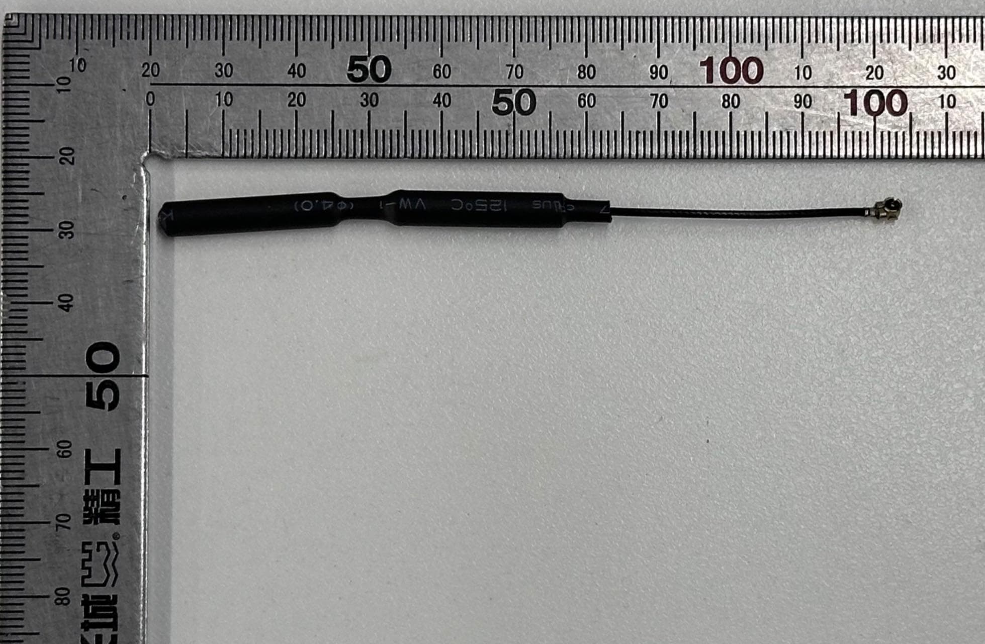
2AFZZ-MHCB12S
Dec 05, 2025Bluetooth Module
Equipment Class
DTS - Digital Transmission System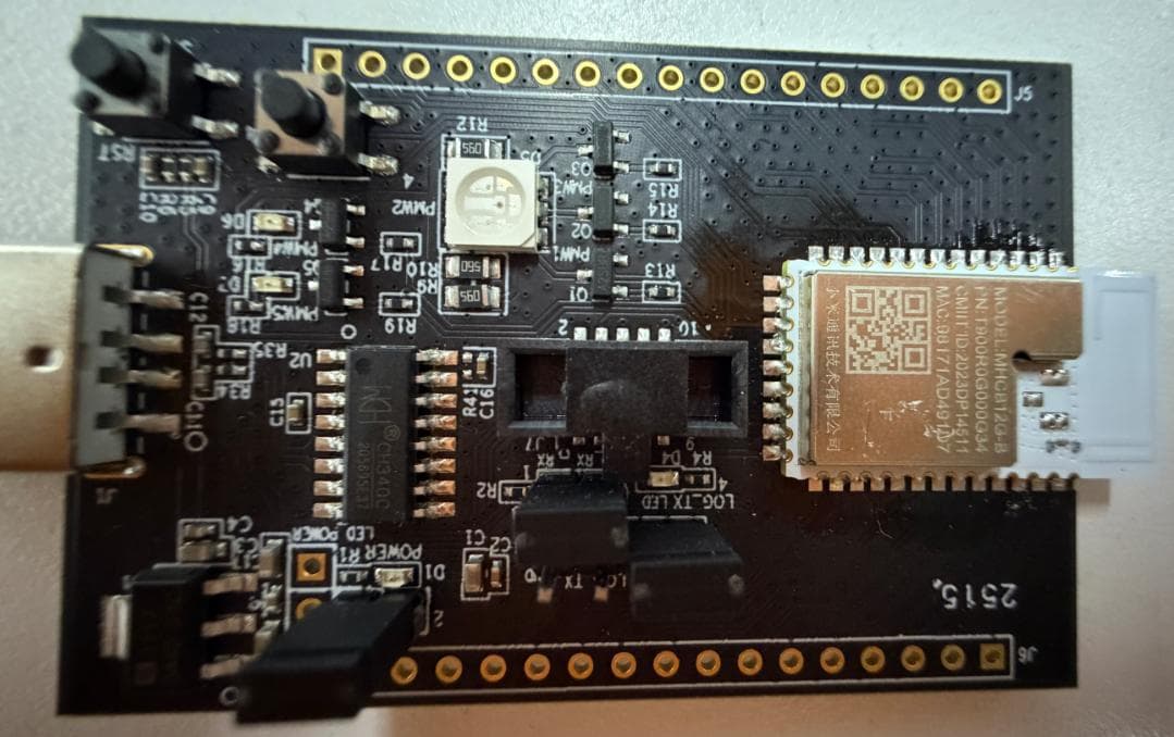
2AFZZ-MHCB12G-B
Dec 05, 2025Bluetooth Module
Equipment Class
DTS - Digital Transmission System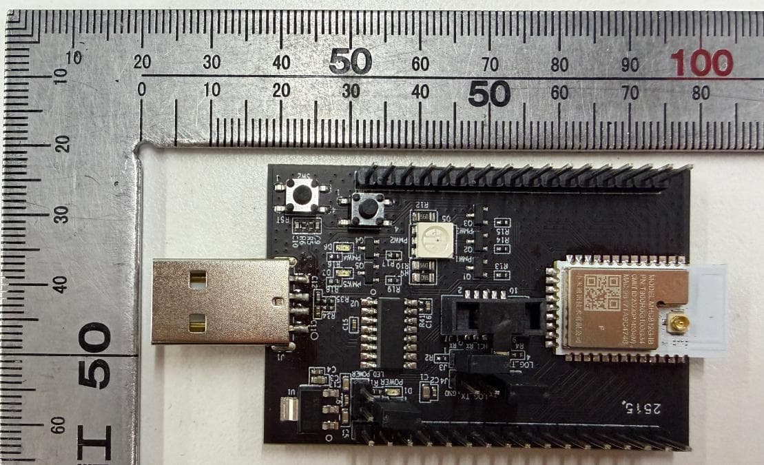
2AFZZ-MHCB12G-IB
Dec 05, 2025Bluetooth Module
Equipment Class
DTS - Digital Transmission System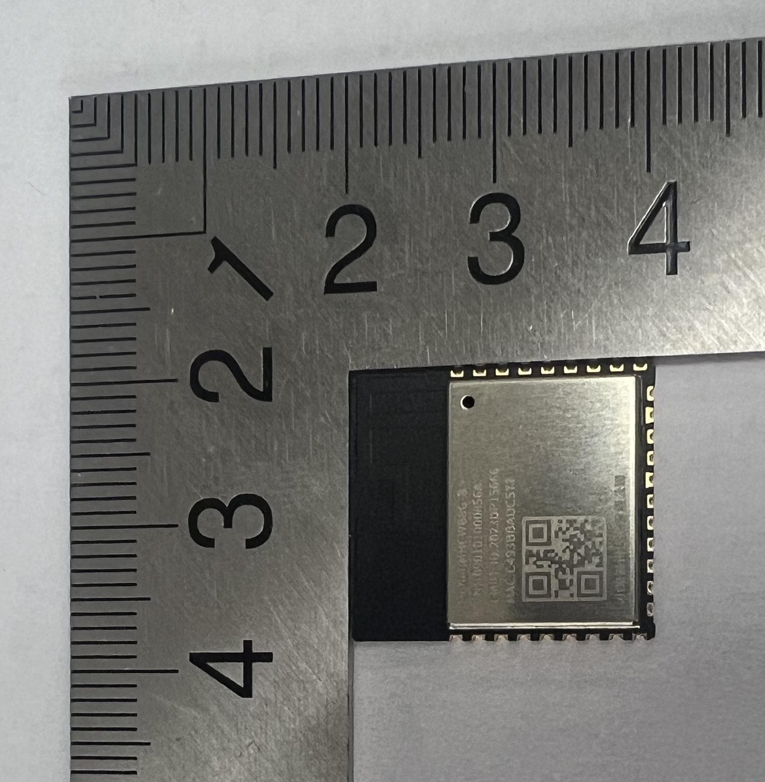
2AFZZ-MHCWB8G-B
Dec 05, 20252.4GHz WIFI+Bluetooth dual-mode module
Equipment Class
DTS - Digital Transmission System