2AMV5SK522-W2-outlet WiFi smart socket
Changxing Potek Electronics & Technology Co., Ltd.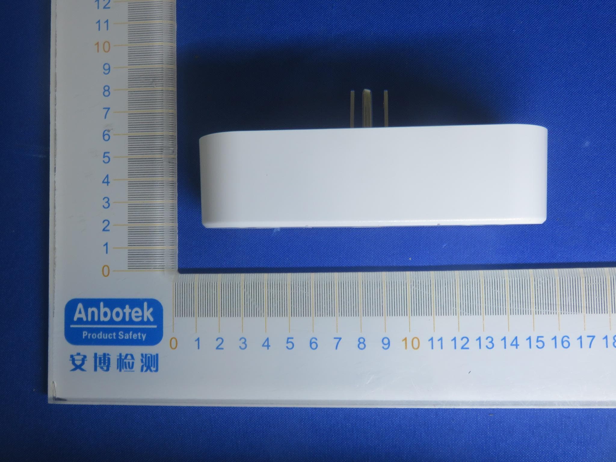
Click to zoom
Application Details
- Equipment Class
- DTS - Digital Transmission System
- Date of Grant
- Feb 02, 2021
- Application Purpose
- Original Equipment
- Date of Application
- Feb 02, 2021
- Equipment Note
- 2-outlet WiFi smart socket
- Frequency Range
- 2412.00000000 - 2462.00000000
- Country
- China
Documents & Files
Document Text
Text extracted from the exhibit documents filed with the FCC. Open a document above to read the original.
Users Manual
SK522-W is a wifi Wireless’s socket , the hardware include two keyswitch, one wifi chip (BK7231) ,two outputs and three blue LEDs.Its working principle is divided into:The Smart Phone control socket through the internet or 4G net. BK7231 responsible for the function keyswitch signals are transmitted to a control part.Control part based on the keyswitch information,control LED and RELAY output ON or OFF. The shell side of the appliance has one button and two indicators. There are two types of keystrokes: tap and long. ·Tap the switch to control the socket, the light is on when on, and off when off; ·Press and hold into the EZ distribution status, the light flashes, at this time can be in accordance with the EZ configuration method for the distribution of the network; ·Press and hold again when flashing, will enter the AP distribution status, the indicator flashes slowly, at this time according to the AP configuration method for the distribution. Note:The SK509-W-2S-N has a power-down memory function thatwill be noted by the device as long as it remains ON or OFFfor5 secondsand will return to this state after the nextpower-up. 1 、 CPU BK7231 is a 2.4 GHz 802.11n chip with multi-media feature. It integrates hardware and software component to finish a complete 802.11b/g/n application, which supports AP and STA role simultaneously. It is able to support multiple cloud links. •Programmable RAM/ROM interfaces (iBus), which can be connected with memory controller, and can also be used to visit flash. •Data RAM interface (dBus), which can connect with memory controller. •AHB interface which can be used to visit theregister. •External 26MHz OSC provide a basic clock speed, Then the clock speed is increased to 80MHz through the internal PLL circuit 2,Memory BK7231 Wi-Fi SoC integrates memory controller and memory units including SRAM and ROM. MCU can access the memory units through iBus, dBus, and AHB interfaces. All memory units can be accessed upon request, while a memory arbiter will decide the running sequence according to the time when these requests are received by the processor. According to our current version of SDK, SRAM space available to users is assigned as below. •RAM size < 50 kB, that is, when BK7231 is working under the Station mode and connects to the router, programmable space accessible in heap + data section is around 50 kB. •There is no programmable ROM in the SoC, therefore, user program must be stored in an external SPI flash. BK7231 uses external SPI flash to store user programs, and supports up to 16 MB memory capacity theoretically. The high frequency clock on BK7231 is used to drive both transmit and receive mixers. This clock is generated from internal crystal oscillator and external crystal. The internal calibration inside the crystal oscillator ensures that a wide range of crystals can be used, nevertheless the quality of the crystal is still a factor to consider to have reasonable phase noise and good Wi-Fi sensitivity. 3,Power Management BK7231 is designed with advanced power management technologies and intended for mobile devices, wearable electronics and the Internet of Things applications. Thelow-powerarchitectureoperatesin3modes:activemode,sleepmodeandDeep sleepmode.BK7231consumesabout7μAofpowerinDeep-sleepmode(withRTC clockstillrunning)andlessthan1.0mA(DTIM=3)orlessthan0.6mA(DTIM=10)to stayconnectedtotheaccesspoint. 2.4 GHz Transceiver The 2.4 GHz receiver down-converts the RF signals to quadrature baseband signals and converts them to the digital domain with 2 high resolution high speed ADCs. To adapt to varying signal channel conditions, RF filters, automatic gain control (AGC), DC offset cancelation circuits and baseband filters are integrated within BK7231. The 2.4 GHz transmitter up-converts the quadrature baseband signals to 2.4 GHz, and drives the antenna with a high-power CMOS power amplifier. The function of digital calibration further improves the linearity of the power amplifier, Additional calibrations are integrated to offset any imperfections of the radio, such as: • Carrier leakage • I/Q phase matching • Baseband nonlinearities •Parameters 1. Operation Temperature: -40°Cto 105°C 2. PCB Material & Size:FR4, 52.2mm x 45mm x 1.2mm 3. RF Modulation: 802.11b,1Mbps (CCK) 802.11g,802.11n20 (OFDM); 4. RF Frequency Range: 2412MHz to 2462MHz; FCC STATEMENT : This device complies with Part 15 of the FCC Rules. Operation is subject to the following two conditions: (1) This device may not cause harmful interference, and (2) This device must accept any interference received, including interference that may cause undesired operation. Warning:Changes or modifications not expressly approved by the party responsible for compliance could void the user's authority to operate the equipment. NOTE: This equipment has been tested and found to comply with the limits for a Class B digital device, pursuant to Part 15 of the FCC Rules. These limits are designed to provide reasonable protection against harmful interference in a residential installation. This equipment generates uses and can radiate radio frequency energy and, if not installed and used in accordance with the instructions, may cause harmful interference to radio communications. However, there is no guarantee that interference will not occur in a particular installation. If this equipment does cause harmful interference to radio or television reception, which can be determined by turning the equipment off and on, the user is encouraged to try to correct the interference by one or more of the following measures: Reorient or relocate the receiving antenna. Increase the separation between the equipment and receiver. Connect the equipment into an outlet on a circuit different from that to which the receiver is connected. Consult the dealer or an experienced radio/TV technician for help. FCC Radiation Exposure Statement: This equipment complies with FCC radiation exposure limits set forth for an uncontrolled environ…
Text truncated - open the document above for the full version.
External Photos
FCCID:2AMV5SK522-W
ID Label/Location Info
LabelLocationOnEUT Label ProductName:2-outletWiFismartsocket ModelNo.:SK522-W FCCID:2AMV5SK522-W ThisdevicecomplieswithPart15oftheFCCRules.Operation issubjecttothefollowingtwoconditions: (1)Thisdevicemaynotcauseharmfulinterference,and (2)Thisdevicemustacceptanyinterferencereceived,including interferencethatmaycauseundesiredoperation.
Internal Photos
FCCID:2AMV5SK522-W WIFIANT
Operational Description
version01 ChangxingPotekElectronics&TechnologyCo.,Ltd. DeclarationconcerningAntennaSpecification Itisherebydeclaredthattheproduct ModelNo.:SK522-W FCCID:2AMV5SK522-W fulfillstherequirementinFCCtestrelatingtotheantennatype. ThedevicespecifiedaboveconfirmstotheFCCrecommendationsforinternalantennatype(s) describedbelow: ModelNo.ofantenna:N/A Typeofantenna:PCBAntenna Gainoftheantenna:0.5dBi Frequencyrange:2412-2462MHz Themountingoftheantennaisfixedtotheradiomoduleandnootherantennashouldbeused. Companyname:ChangxingPotekElectronics&TechnologyCo.,Ltd. Address:No.1218,TaihuAvenue,TaihuSubdistrict,ChangxingCounty,HuzhouCity,Zhejiang, P.R.C. City:HuzhouCity ZIP/Postalcode:N/A Country:China Place:ChinaDate: 2021-02-02 Signature:
RF Exposure Info
RFEXPOSUREEVALUATION AccordingtoFCC1.1310:Thecriterialistedinthefollowingtableshallbeusedto evaluatetheenvironmentimpactofhumanexposuretoradiofrequency(RF)Radiation asspecifiedin§1.1307(b) FCCID:2AMV5SK522-W EUTSpecification EUT2-outletWiFismartsocket Frequencyband(Operating) WLAN:2.412GHz~2.462GHz WLAN:5.18GHz~5.32GHz/5.50GHz~5.70GHz WLAN:5.745GHz~5825GHz Others: DevicecategoryPortable(<20cmseparation) Mobile(>20cmseparation) Others___ ExposureclassificationOccupational/Controlledexposure(S=5mW/cm2) GeneralPopulation/Uncontrolledexposure(S=1mW/cm2) AntennadiversitySingleantenna Multipleantennas Txdiversity Rxdiversity Tx/Rxdiversity Max.outputpower14.57dBm(0.0286W) Antennagain(Max)0.5dBi EvaluationappliedMPEEvaluation SAREvaluation LimitsforMaximumPermissibleExposure(MPE) Frequency Range(MHz) ElectricField Strength(V/m) MagneticField Strength(A/m) Power Density(mW/cm 2 ) Average Time (A)LimitsforOccupational/ControlExposures 300-1500----F/3006 1500-100000----56 (B)LimitsforGeneralPopulation/UncontrolExposures 300-1500----F/15006 1500-100000----130 Friistransmissionformula:Pd=(Pout*G)\(4*pi*R2) Where Pd=PowerdensityinmW/cm 2 Pout=outputpowertoantennainMw G=gainofantennainlinearscale Pi=3.1416 R=distancebetweenobservationpointandcenteroftheradiatorincm PdthelimitofMPE,1mW/cm2.Ifweknowthemaximumgainoftheantennaand totalpowerinputtotheantenna,throughthecalculation,wewillknowthedistance wheretheMPElimitisreached. MeasurementResult Operating Mode Channel Frequency Measured Power Tuneup tolerance Max.Tune upPower Antenna Gain Powerdensity at20cm Power density Limits (mW/cm2) (MHz)(dBm)(dBm)(dBm)(dBi)(mW/cm2) 802.11b 2412 12.8112.81 ±1 13.81 0.50.00541 243712.7812.78±113.780.50.00531 2462 12.8412.84 ±1 13.84 0.50.00541 802.11g 2412 13.3913.39 ±1 14.39 0.50.00611 2437 13.1713.17 ±1 14.17 0.50.00581 2462 13.8913.89 ±1 14.89 0.50.00691 802.11n(20) 241214.5414.54±115.540.50.00801 2437 14.5014.50 ±1 15.5 0.50.00791 2462 14.5714.57 ±1 15.57 0.50.00811
Test Report
Report No.: 18220WC00188301FCC ID: 2AMV5SK522-WPage 1 of 53 Code:AB-RF-05-a FCC TEST REPORT Client Name:Changxing Potek Electronics & Technology Co., Ltd. Address: No. 1218, Taihu Avenue, Taihu Subdistrict, Changxing County, Huzhou, Zhejiang 313199, China Product Name:2-outlet WiFi smart socket Date:Jan. 27, 2021 Shenzhen Anbotek Compliance Laboratory Limited Report No.: 18220WC00188301FCC ID: 2AMV5SK522-WPage 2 of 53 Code:AB-RF-05-a Contents 1. General Information ............................................................................................................................................... 5 1.1. Client Information ....................................................................................................................................... 5 1.2. Description of Device (EUT) ..................................................................................................................... 5 1.3. Auxiliary Equipment Used During Test ................................................................................................... 6 1.4. Description of Test Modes ........................................................................................................................ 6 1.5. List of channels ........................................................................................................................................... 7 1.6. Description Of Test Setup ......................................................................................................................... 8 1.7. Test Equipment List .................................................................................................................................... 9 1.8. Measurement Uncertainty ....................................................................................................................... 10 1.9. Description of Test Facility ...................................................................................................................... 10 2. Summary of Test Results ................................................................................................................................... 11 3. Conducted Emission Test ................................................................................................................................... 12 3.1. Test Standard and Limit .......................................................................................................................... 12 3.2. Test Setup .................................................................................................................................................. 12 3.3. Test Procedure .......................................................................................................................................... 12 4. Radiation Spurious Emission and Band Edge ................................................................................................ 15 4.1. Test Standard and Limit .......................................................................................................................... 15 4.2. Test Setup .................................................................................................................................................. 15 4.3. Test Procedure .......................................................................................................................................... 16 4.4. Test Data .................................................................................................................................................... 17 5. Maximum Output Power Test ............................................................................................................................ 26 5.1. Test Standard and Limit .......................................................................................................................... 26 5.2. Test Setup .................................................................................................................................................. 26 5.3. Test Procedure .......................................................................................................................................... 26 5.4. Test Data .................................................................................................................................................... 26 6. 6DB Occupy Bandwidth Test ............................................................................................................................. 30 6.1. Test Standard and Limit .......................................................................................................................... 30 6.2. Test Setup .................................................................................................................................................. 30 6.3. Test Procedure .......................................................................................................................................... 30 6.4. Test Data .................................................................................................................................................... 30 7. Power Spectral Density Test .............................................................................................................................. 37 7.1. Test Standard and Limit .......................................................................................................................... 37 7.2. Test Setup .................................................................................................................................................. 37 7.3. Test Procedure .......................................................................................................................................... 37 7.4. Test Data ............................................................................................................…
Text truncated - open the document above for the full version.
Test Setup Photos
FCCID:2AMV5SK522-W PhotoofPowerLineConductedEmissionTest PhotoofRadiationEmissionTest
Contact Information
Applicant
FIONA WEN(SALES V.P.)
Test Firm
Shenzhen Anbotek Compliance Laboratory LimitedJeff Zhu
Technical Specifications
| # | Rule Parts | Frequency Range | Power Output |
|---|---|---|---|
| 1 | 15C | 2.41 GHz - 2.46 GHz | 28.60 mW |
Other Applications from Changxing Potek Electronics & Technology Co., Ltd.
2AMV5-SK569-WU-AC
Jul 24, 2023Smart Power Strip
Equipment Class
DTS - Digital Transmission System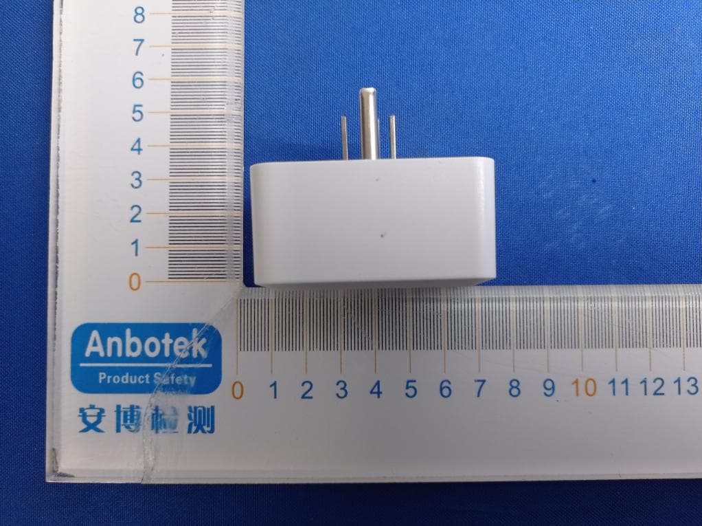
2AMV5-SK543-W-A
Jul 28, 20211-outlet indoor wifi smart plug
Equipment Class
DTS - Digital Transmission System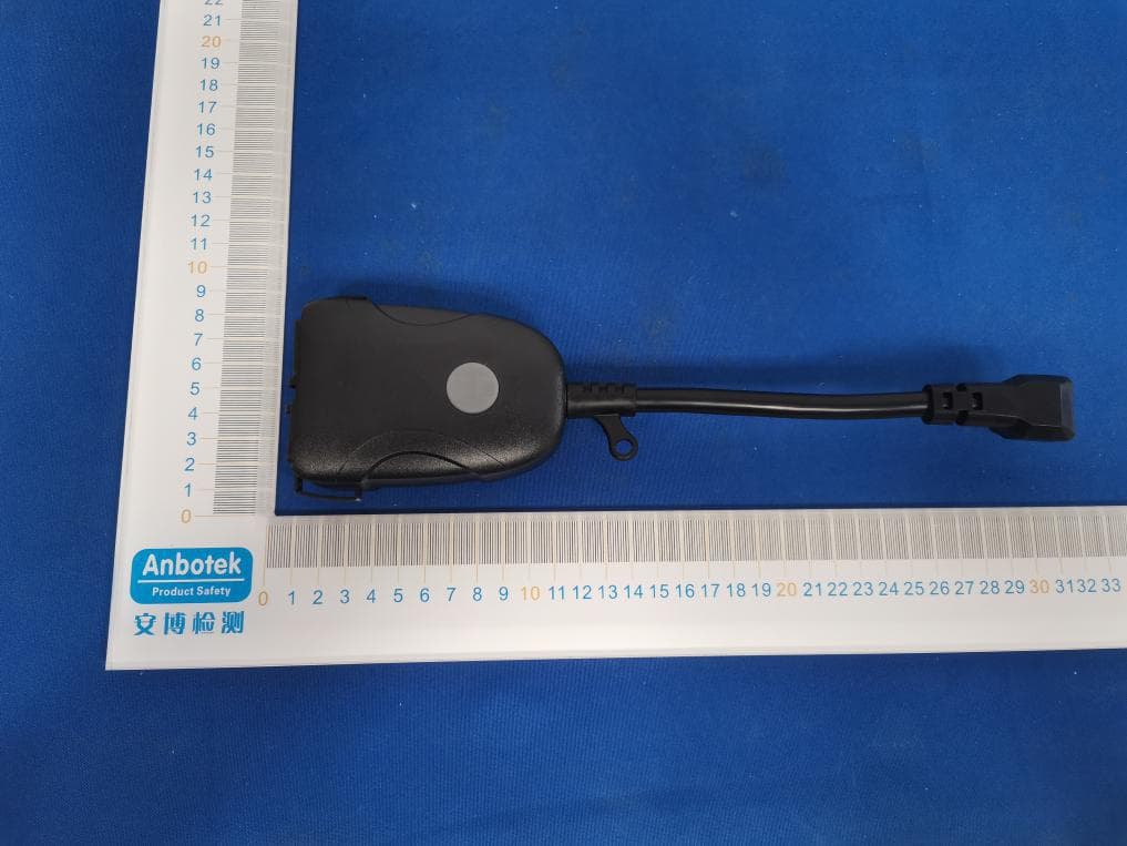
2AMV5-SK509WN
Jul 22, 20212-outlet outdoor wifi smart plug
Equipment Class
DTS - Digital Transmission System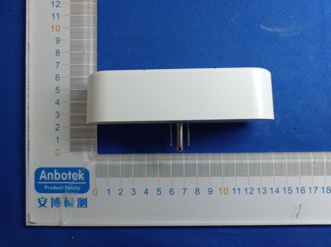
2AMV5-SK521-W-A
Jun 30, 20212-outlet simultaneously controlled indoor wifi smart plug
Equipment Class
DTS - Digital Transmission System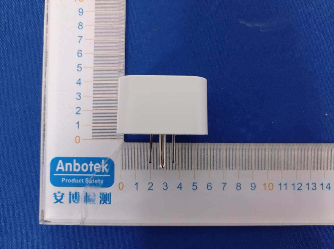
2AMV5-SK539-W-A
Jun 30, 20211-outlet indoor wifi smart plug
Equipment Class
DTS - Digital Transmission System