2APZE-F400Bluetooth headset
Shenzhen FuShiKe Electronic Co., Ltd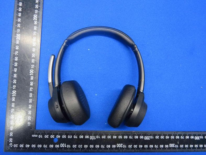
Click to zoom
Application Details
- Equipment Class
- DSS - Part 15 Spread Spectrum Transmitter
- Date of Grant
- Jun 30, 2024
- Application Purpose
- Original Equipment
- Date of Application
- Jun 30, 2024
- Equipment Note
- Bluetooth headset
- Frequency Range
- 2402.00000000 - 2480.00000000
- Country
- China
Documents & Files
Document Text
Text extracted from the exhibit documents filed with the FCC. Open a document above to read the original.
Users Manual
Device name MUTE Size: 288*91mm 10M Wireless Headset We are appreciated for purchasing our wireless headset. This guide contains instructions for setting up and using your headset easily. 5s 1. Enable pairing model: Hold the multi-function button for 4s after power on. 2. Power on: Turn the power button to ON state. 3. Power off: Turn the power button to OFF state. 4. Recover default settings: When charging, hold the Multi-function Button for about 4s till the blue indicator flashesto recover default settings. Pair with 2 phones 3H Hold on 2s FCC Warnning: This equipment has been tested and found to comply with the limits for a Class B digital device, pursuant to part 15 of the FCC Rules. These limits are designed to provide reasonable protection againstharmful interference in a residential installation. This equipment generates, uses and can radiateradio frequency energy and, if not installed and used in accordance with the instructions, maycause harmful interference to radio communications. However, there is no guarantee thatinterference will not occur in a particular installation. If this equipment does cause harmfulinterference to radio or television reception, which can be determined by turning the equipmentoff and on, the user is encouraged to try to correct the interference by one or more of thefollowing measures: • Reorient or relocate the receiving antenna. • Increase the separation between the equipment and receiver. • Connect the equipment into an outlet on a circuit different from that to which the receiver is connected. • Consult the dealer or an experienced radio/TV technician for help. Caution: Any changes or modifications to this device not explicitly approved by manufacturer could void your authority to operate this equipment. This device complies with part 15 of the FCC Rules. Operation is subject to the following two conditions: (1)This device may not cause harmful interference, and (2) this device must accept any interference received, including interference that may cause undesired operation. This equipment complies with FCC radiation exposure limits set forth for an uncontrolled environment. This equipment should be installed and operated with minimum distance 0cm between the radiator and your body.
Attestation Statements
Shenzhen FuShiKe Electronic Co., Ltd 3/F, No.8, Xinhu South Street, Xintian, Guanlan Street, Longhua District,Shenzhen China Federal Communications Commission Authorization and Evaluation Division Equipment Authorization Branch 7435 Oakland Mills Road Columbia, MD 21046 2024-6-29 To whom it may concern: We, Shenzhen FuShiKe Electronic Co., Ltd, hereby certify that the equipment for which authorization is sought (FCC ID: 2APZE-F400) is not “covered” equipment prohibited from receiving an equipment authorization pursuant to § 2.903 of the FCC rules. We also certify that, as of the date of the filing of the application, we are not identified on the Covered List (https://www.fcc.gov/supplychain/coveredlist) as an entity producing “covered” equipment. By signing this form, we confirm the above and that we are aware of the application requirements listed under § 2.911(b) and (d)(5) and (6). The information provided in this letter is based on the referenced rule parts of Title 47 of the CFR as well as KDB 986446 D01. Sincerely, Signature XiaoHuang Yan Manager Shenzhen FuShiKe Electronic Co., Ltd 62_[model] CoveredEqu_2.911(d)(5)(i) and (ii) - U, V03
Cover Letter(s)
CONFIDENTIALITY REQUEST for Certification Service in USA Federal Communication Commission Equipment Authorization Division, Application Processing Branch 7435 Oakland Mills Road Columbia, MD 21046 Date:<2024-6-29> Pursuant to Paragraphs §0.457 and 0.459 of the Commission’s Rules (47 C.F.R.) and Section §552(b)(4) of the Freedom of Information Act, we requests confidentiality for the following products: FCC ID Model name 2APZE-F400 F400 For the product stated above, we request that the following information be held confidential; Exhibits Long-Term Confidentiality Short-Term Confidentiality Short-Term Confidentiality Days External Photos Internal Photos Block Diagram Schematics Test Setup Photos User’s Manual Parts List Tune Up Operational Descriptions The long-term confidentiality exhibits contain our trade secrets and proprietary information that could be of benefit to our competitors. The short-term confidentiality on the basis of ensuring that business sensitive information remains confidential until the actual marketing of our new device. If you have any questions, please feel free to contact me at the address shown below. Sincerely, Name/Title: XiaoHuang Yan/Manager Company: Shenzhen FuShiKe Electronic Co., Ltd Address: 3/F, No.8, Xinhu South Street, Xintian, Guanlan Street, Longhua District,Shenzhen China Phone: +86-0755-29805984 Fax: N/A E-Mail: [email protected]
Cover Letter(s)
Shenzhen FuShiKe Electronic Co., Ltd 3/F, No.8, Xinhu South Street, Xintian, Guanlan Street, Longhua District,Shenzhen China Federal Communications Commission Authorization and Evaluation Division Equipment Authorization Branch 7435 Oakland Mills Road Columbia, MD 21046 2024-6-29 To whom it may concern: We, the undersigned, hereby authorize Eurofins Product Service GmbH to act on our behalf in all matters relating to applications for equipment authorization FCC ID: 2APZE-F400 including the signing of all documents related to these matters. Any and all acts carried out by Eurofins Product Service GmbH on our behalf shall have the same effect as acts of our own. By signing this application form, we agree to Eurofins’ current valid General Terms and Conditions (AGB),Testing and Certification Regulations (PZO) which can be viewed on following website www.eurofins.de/ee or retrieved on request. We also hereby certify that no party to this application is subject to a denial of benefits, including FCC benefits, pursuant to Section 5301 of the Anti-Drug Abuse Act of 1988, 21 U.S.C. 862. Sincerely, Name/Title: XiaoHuang Yan/Manager Company: Shenzhen FuShiKe Electronic Co., Ltd Address: 3/F, No.8, Xinhu South Street, Xintian, Guanlan Street, Longhua District,Shenzhen China Phone: +86-0755-29805984 Fax: N/A E-Mail: [email protected]
External Photos
Shenzhen HTT Technology Co., Ltd. Report No.: HTT202406295 Shenzhen HTT Technology Co.,Ltd. Tel: 0755-23595200 Fax: 0755-23595201 1F, Building B, Huafeng International Robotics Industrial Park,Hangcheng Road, Nanchang Community, Xixiang Street, Bao'an District, Guangdong Province, Shenzhen, China Page 1 of 3 Product Name: Bluetooth headset Model No.: F400 EUT Constructional Details External Photo Report No.: HTT202406295 Shenzhen HTT Technology Co.,Ltd. Tel: 0755-23595200 Fax: 0755-23595201 1F, Building B, Huafeng International Robotics Industrial Park,Hangcheng Road, Nanchang Community, Xixiang Street, Bao'an District, Guangdong Province, Shenzhen, China Page 2 of 3 Report No.: HTT202406295 Shenzhen HTT Technology Co.,Ltd. Tel: 0755-23595200 Fax: 0755-23595201 1F, Building B, Huafeng International Robotics Industrial Park,Hangcheng Road, Nanchang Community, Xixiang Street, Bao'an District, Guangdong Province, Shenzhen, China Page 3 of 3 ------End------
ID Label/Location Info
Label and Location Size: L: 1.0cm*W: 0.2cm Label and Location FCC ID : 2APZE-F400
Internal Photos
Shenzhen HTT Technology Co., Ltd. Report No.: HTT202406295 Shenzhen HTT Technology Co.,Ltd. Tel: 0755-23595200 Fax: 0755-23595201 1F, Building B, Huafeng International Robotics Industrial Park,Hangcheng Road, Nanchang Community, Xixiang Street, Bao'an District, Guangdong Province, Shenzhen, China Page 1 of 3 Product Name: Bluetooth headset Model No.: F400 EUT Constructional Details Internal Photo Report No.: HTT202406295 Shenzhen HTT Technology Co.,Ltd. Tel: 0755-23595200 Fax: 0755-23595201 1F, Building B, Huafeng International Robotics Industrial Park,Hangcheng Road, Nanchang Community, Xixiang Street, Bao'an District, Guangdong Province, Shenzhen, China Page 2 of 3 Report No.: HTT202406295 Shenzhen HTT Technology Co.,Ltd. Tel: 0755-23595200 Fax: 0755-23595201 1F, Building B, Huafeng International Robotics Industrial Park,Hangcheng Road, Nanchang Community, Xixiang Street, Bao'an District, Guangdong Province, Shenzhen, China Page 3 of 3 ------End------
RF Exposure Info
RF Exposure evaluation FCC ID: 2APZE-F400 1.1. Applicable Standard According to §1.1307(b)(1), systems operating under the provisions of this section shall be operated in a manner that ensures that the public is not exposed to radio frequency energy level in excess of the Commission’s guidelines. According to §1.1310 and §2.1093 RF exposure requirement KDB447498 v06: Mobile and Portable Devices RF Exposure Procedures and Equipment Authorization Policies 1.2. Requirement According to KDB447498 D01 General RF Exposure Guidance v06 Section 4.3.1 Standalone SAR test exclusion considerations: “Unless specifically required by the published RF exposure KDB procedures, standalone 1-g head or body and 10-g extremity SAR evaluation for general population exposure conditions, by measurement or numerical simulation, is not required when the corresponding SAR Test Exclusion Threshold condition, listed below, is satisfied. These test exclusion conditions are based on source-based time-averaged maximum conducted output power of the RF channel requiring evaluation, adjusted for tune-up tolerance, and the minimum test separation distance required for the exposure conditions.22 The minimum test separation distance is determined by the smallest distance from the antenna and radiating structures or outer surface of the device, according to the host form factor, exposure conditions and platform requirements, to any part of the body or extremity of a user or bystander (see 5) of section 4.1). To qualify for SAR test exclusion, the test separation distances applied must be fully explained and justified by the operating configurations and exposure conditions of the transmitter and applicable host platform requirements, typically in the SAR measurement or SAR analysis report, according to the required published RF exposure KDB procedures. When no other RF exposure testing or reporting is required, a statement of justification and compliance must be included in the equipment approval, in lieu of the SAR report, to qualify for the SAR test exclusion. When required, the device specific conditions described in the other published RF exposure KDB procedures must be satisfied before applying these SAR test exclusion provisions; for example, handheld PTT two-way radios, handsets, laptops & tablets etc.23 “ [(max. power of channel, including tune-up tolerance, mW)/ (min. test separation distance, mm)] · [√f (GHz)] ≤ 3.0 for 1-g SAR and ≤ 7.5 for 10-g extremity SAR, where: • f (GHz) is the RF channel transmit frequency in GHz • Power and distance are rounded to the nearest mW and mm before calculation • The result is rounded to one decimal place for comparison • 3.0 and 7.5 are referred to as the numeric thresholds in the step 2 below The test exclusions are applicable only when the minimum test separation distance is ≤ 50 mm and for transmission frequencies between 100 MHz and 6 GHz. When the minimum test separation distance is < 5 mm, a distance of 5 mm according to 5) in section 4.1 is applied to determine SAR test exclusion. 1.3. Manufacturing tolerance GFSK (Peak) Channel Channel 0 Channel 39 Channel 78 Target (dBm) -1.0 -2.0 -2.0 Tolerance ±(dB) 1.0 1.0 1.0 π/4DQPSK (Peak) Channel Channel 0 Channel 39 Channel 78 Target (dBm) 0.0 0.0 0.0 Tolerance ±(dB) 1.0 1.0 1.0 8-DPSK (Peak) Channel Channel 0 Channel 39 Channel 78 Target (dBm) 1.0 0.0 0.0 Tolerance ±(dB) 1.0 1.0 1.0 Page 2 of 2 2. E v a l u a t i o n R e s u l t Evaluation Results Band/Mode f (GHz) Antenna Distance (mm) RF output power (including tune-up tolerance) SAR Test Exclusion Threshold SAR Test Exclusion dBm mW BT 2.450 5 2.0 1.5849 0.4962<3.0 Yes 3. C o n c l u s i o n The measurement results comply with the FCC Limit per 47 CFR 2.1093 for the uncontrolled RF Exposure and SAR Exclusion Threshold per KDB 447498 v06 .....................End of Report.........................
Test Report
2.4GHz Chip Antenna: AAN3216H4R2G45 ______________________________________________________________________________________________________ Application: WLAN, 802.11b/g, Bluetooth, etc... Features SMD, high reliability, ultra Impact, Omni-directional... Electrical Specification Working Frequency Range 2400 ~2484 MHz Peak Gain 3.0dBi (Typ.) Impedance 50 Ohm Return loss 10 dB ( Min) Polarization Linear Azimuth Beamwidth Omni-directional Operation Temperature(°C) -40 ~85°C The specification is defined on EVB. Dimension and Terminal Configuration Part number AAN 3216 H4 R 2G45 (1) (2) (3) (4) (5) (1)Product Type Chip Antenna (2) Size Code 3.2x1.6mm (3) Type Code H4 (4) Packing Tape and reel (5) Frequency 2.45GHz Dimension (mm) No. Terminal Name L 3.2 +-0.20 1 Feeding W 1.6+-0.20 2 Soldering T 1.20+-0.20 A 0.20+-0.20 2.4GHz 2.45HHz Chip Antenna: AAN3216H4R2G45 ______________________________________________________________________________________________________ Evaluation Board Reference PCB Dimension & Antenna Layout Reference unit :mm Electrical Characteristics Return Loss & Radiation Return Loss Frequency (MHz) S11 (dB) 2400 -12.8 2442 -19.8 2484 -11.9 Radiation 2.45GHz Frequency 2445MHz Peak gain 3.0dBi Efficiency 79.2% 2.4GHz 2.45HHz Chip Antenna: AAN3216H4R2G45 ______________________________________________________________________________________________________ Taping Specifications Reel Taping Blister Tape Checking note Index Spec (mm) Internal diameter of reel A 60.20 ± 0.50 External diameter of reel B 178 ± 1.00 Quantity/per reel 2500 pcs Tape material Plastic (embossed) Checking note Index Spec (mm) Sprocket hole D0 1.50 +0.10/-0.00 Distance sprocket hole to outside E1 1.75 ± 0.10 Distance sprocket hole to pocket F 5.50 ± 0.05 Distance sprocket hole to sprocket hole P0 4.00 ± 0.10 Distance pocket to pocket P1 4.00 ± 0.10 Distance sprocket hole to pocket P2 2.00 ± 0.05 Tape width W 12.00 +0.30/-0.10 Pocket width nominal clearance A0 2.28 ± 0.13 Pocket length nominal clearance B0 5.70 ± 0.13 Pocket depth minimum clearance K0 1.58 ± 0.10 Thickness of tape T 0.23 ± 0.02 2.4GHz 2.45HHz Chip Antenna: AAN3216H4R2G45 ______________________________________________________________________________________________________ Reliability Table Test ItemProcedure Requirements Ceramic Type Remark (Reference) Electrical Characterization Fulfill the electrical specification User Spec. Thermal Shock 1. Preconditioning: 50 ± 10°C / 1 hr , then keep for 24 ± 1 hrs at room temp. 2. Initial measure: Spec: refer Initial spec. 3. Rapid change of temperature test: -30°C to +85°C; 100 cycles; 15 minutes at Lower category temperature; 15 minutes at Upper category temperature. No Visible Damage. Fulfill the electrical specification. MIL-STD-202 107 Temperature Cycling 1. Initial measure: Spec: refer Initial spec. 2. 100 Cycles (-30°C to +85°C), Soak Mode=1 (2 Cycle/hours). 3. Measurement at 24 ± 2Hours after test condition. No Visible Damage. Fulfill the electrical specification. JESD22 JA104 High Temperature Exposure 1. Initial measure: Spec: refer Initial spec. 2. Unpowered; 500hours @ T=+85°C. 3. Measurement at 24 ± 2 hours after test. No Visible Damage. Fulfill the electrical specification. MIL-STD-202 108 Low Temperature Storage 1. Initial measure: Spec: refer Initial spec. 2. Unpowered: 500hours @ T= -30°C. 3. Measurement at 24 ± 2 hours after test. No Visible Damage. Fulfill the electrical specification. MIL-STD-202 108 Solderability (SMD Bottom Side) Dipping method: a. Temperature: 235 ± 5°C b. Dipping time: 3 ± 0.5s The solder should cover over 95% of the critical area of bottom side. IEC 60384-21/22 4.10 Soldering Heat Resistance (RSH) Preheating temperature: 150 ± 10°C. Preheating time: 1~2 min. Solder temperature: 260 ± 5°C. Dipping time: 5 ± 0.5s No Visible Damage.IEC 60384-21/22 4.10 Vibration5g's for 20 min., 12 cycles each of 3 orientations Note: Use 8"X5" PCB .031" thick 7 secure points on, one long side and 2 secure points at corners of opposite sides. Parts mounted within 2" from any secure point. Test from 10-2000 Hz. No Visible Damage.MIL-STD-202 Method 204 Mechanical Shock Three shocks in each direction shall be applied along the three mutually perpendicular axes of the test specimen (18 shocks) Peak value: 1,500g’s Duration: 0.5ms Velocity change: 15.4 ft/s Waveform: Half-sine No Visible Damage.MIL-STD-202 Method 213 Humidity Bias 1. Humidity: 85% R.H., Temperature: 85 ± 2 °C. 2. Time: 500 ± 24 hours. 3. Measurement at 24 ± 2hrs after test condition. No Visible Damage. Fulfill the electrical specification. MIL-STD-202 Method 106 2.4GHz 2.45HHz Chip Antenna: AAN3216H4R2G45 ______________________________________________________________________________________________________ Revision History Revision Date Content 1 2019/7/26New issue Board Flex (SMD) 1. Mounting method: IR-Reflow. PCB Size (L:100 × W:40 × T:1.6mm) 2. Apply the load in direction of the arrow until bending reaches 2 mm. No Visible Damage.AEC-Q200 005 AdhesionForce of 1.8Kg for 60 seconds.No Visible Damage Magnification of 20X or greater may be employed for inspection of the mechanical integrity of the device body terminals and body/terminal junction. AEC-Q200 006 Physical Dimension Any applicable method using x10 magnification, micrometers, calipers, gauges, contour projectors, or other measuring equipment, capable of determining the actual specimen dimensions. In accordance with specification. JESD22 JB100
Test Report
Shenzhen HTT Technology Co., Ltd. Report No.: HTT202406295F01 This results shown in this test report refer only to the sample(s) tested, this test report cannot be reproduced, except in full, without prior written permission of the company. The report would be invalid without specific stamp of test institute and the signatures of compiler and approver. Page 1 of 45 TEST Report Applicant: Shenzhen FuShiKe Electronic Co., Ltd Address of Applicant: 3/F, No.8, Xinhu South Street, Xintian, Guanlan Street, Longhua District, Shenzhen, China 518110 Manufacturer : Shenzhen FuShiKe Electronic Co., Ltd Address of Manufacturer : 3/F, No.8, Xinhu South Street, Xintian, Guanlan Street, Longhua District, Shenzhen, China 518110 Equipment Under Test (EUT) Product Name: Bluetooth headset Model No.: F400 Series model: N/A Trade Mark: N/A FCC ID: 2APZE-F400 Applicable standards: FCC CFR Title 47 Part 15 Subpart C Section 15.247 Date of sample receipt: Jun. 12, 2024 Date of Test: Jun. 12, 2024 ~ Jun. 18, 2024 Date of report issued: Jun. 18, 2024 Test Result : PASS * * In the configuration tested, the EUT complied with the standards specified above. Report No.: HTT202406295F01 Shenzhen HTT Technology Co.,Ltd. Tel: 0755-23595200 Fax: 0755-23595201 1F, Building B, Huafeng International Robotics Industrial Park, Hangcheng Road,Nanchang Community, Xixiang Street, Bao'an District, Shenzhen, Guangdong, China Page 2 of 45 1. Version Version No. Date Description 00 Jun. 18, 2024 Original Tested/ Prepared By Date: Jun. 18, 2024 Project Engineer Check By: Date: Jun. 18, 2024 Reviewer Approved By : Date: Jun. 18, 2024 Authorized Signature Report No.: HTT202406295F01 Shenzhen HTT Technology Co.,Ltd. Tel: 0755-23595200 Fax: 0755-23595201 1F, Building B, Huafeng International Robotics Industrial Park, Hangcheng Road,Nanchang Community, Xixiang Street, Bao'an District, Shenzhen, Guangdong, China Page 3 of 45 2. Contents Page 1. VERSION ........................................................................................................................................................ 2 2. CONTENTS .................................................................................................................................................... 3 3. TEST SUMMARY ........................................................................................................................................... 4 4. GENERAL INFORMATION ............................................................................................................................ 5 4.1. GENERAL DESCRIPTION OF EUT ................................................................................................................ 5 4.2. TEST MODE ............................................................................................................................................... 7 4.3. DESCRIPTION OF SUPPORT UNITS .............................................................................................................. 7 4.4. DEVIATION FROM STANDARDS .................................................................................................................... 7 4.5. ABNORMALITIES FROM STANDARD CONDITIONS ........................................................................................... 7 4.6. TEST FACILITY ........................................................................................................................................... 7 4.7. TEST LOCATION ......................................................................................................................................... 7 4.8. ADDITIONAL INSTRUCTIONS ........................................................................................................................ 7 5. TEST INSTRUMENTS LIST ........................................................................................................................... 8 6. TEST RESULTS AND MEASUREMENT DATA ........................................................................................... 9 6.1. CONDUCTED EMISSIONS ............................................................................................................................ 9 6.2. CONDUCTED PEAK OUTPUT POWER ......................................................................................................... 12 6.3. 20DB EMISSION BANDWIDTH .................................................................................................................... 13 6.4. FREQUENCIES SEPARATION ..................................................................................................................... 17 6.5. HOPPING CHANNEL NUMBER .................................................................................................................... 19 6.6. DWELL TIME ............................................................................................................................................ 21 6.7. BAND EDGE ............................................................................................................................................. 26 6.7.1. Conducted Emission Method ......................................................................................................... 26 6.7.2. Radiated Emission Method ............................................................................................................ 30 6.8. SPURIOUS EMISSION ................................................................................................................................ 32 6.8.1. Conducted Emission Method ......................................................................................................... 32 6.8.2. Radiated Emission Method ............................................................................................................ 37 6.9. ANTENNA REQUIREMENT .......................................................................................................................... 44 7. TEST…
Text truncated - open the document above for the full version.
Test Setup Photos
Shenzhen HTT Technology Co., Ltd. Report No.: HTT202406295 Shenzhen HTT Technology Co.,Ltd. Tel: 0755-23595200 Fax: 0755-23595201 1F, Building B, Huafeng International Robotics Industrial Park,Hangcheng Road, Nanchang Community, Xixiang Street, Bao'an District, Guangdong Province, Shenzhen, China Page 1 of 2 Product Name: Bluetooth headset Model No.: F400 Test Setup Photo Radiated Emission Report No.: HTT202406295 Shenzhen HTT Technology Co.,Ltd. Tel: 0755-23595200 Fax: 0755-23595201 1F, Building B, Huafeng International Robotics Industrial Park,Hangcheng Road, Nanchang Community, Xixiang Street, Bao'an District, Guangdong Province, Shenzhen, China Page 2 of 2 Conducted Emission ------End------
Contact Information
Applicant
XiaoHuang Yan(General Manager)
Test Firm
Shenzhen HTT Technology Co.,Ltd.Kevin Yang
[email protected]86-755-23595200
Technical Specifications
| # | Rule Parts | Frequency Range | Power Output |
|---|---|---|---|
| 1 | 15C | 2.40 GHz - 2.48 GHz | 1.40 mW |
Other Applications from Shenzhen FuShiKe Electronic Co., Ltd
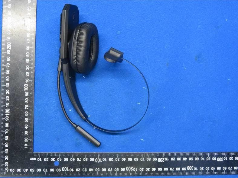
2APZE-A18
Aug 21, 2024Bluetooth headset
Equipment Class
DSS - Part 15 Spread Spectrum Transmitter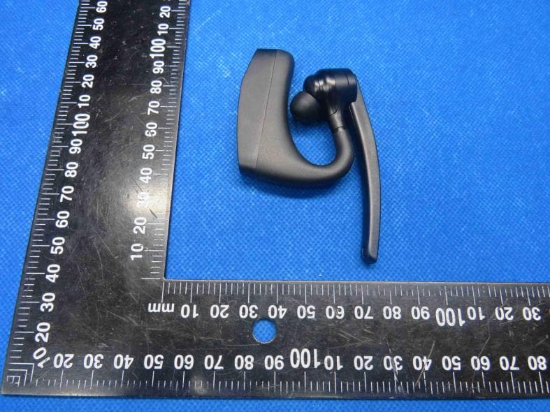
2APZE-K30
Jul 14, 2023Bluetooth headset
Equipment Class
DSS - Part 15 Spread Spectrum Transmitter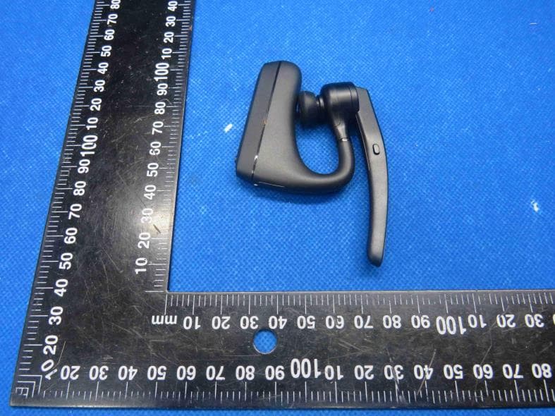
2APZE-K22
Jul 14, 2023Bluetooth headset
Equipment Class
DSS - Part 15 Spread Spectrum Transmitter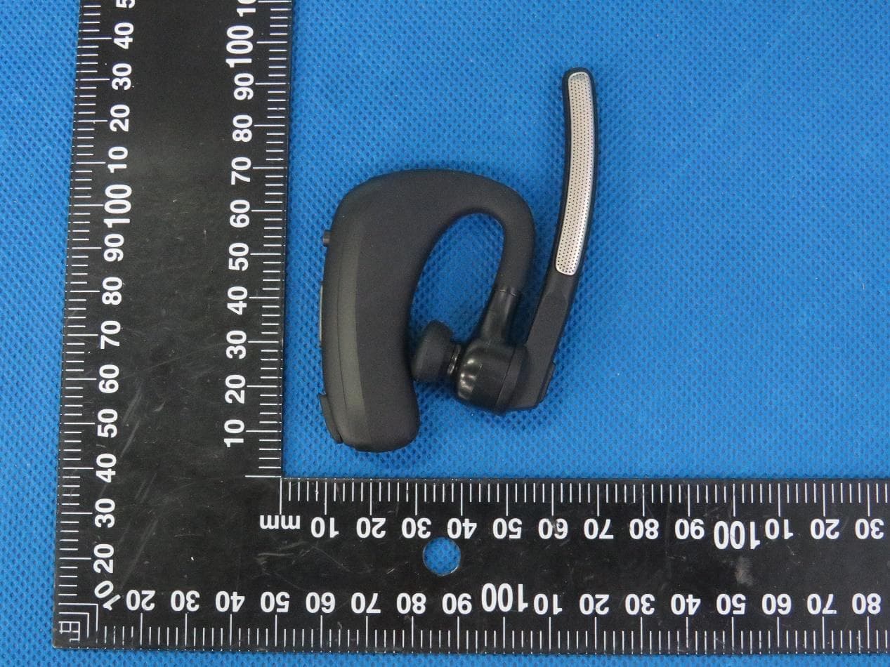
2APZE-K20
May 20, 2021Bluetooth headset
Equipment Class
DTS - Digital Transmission System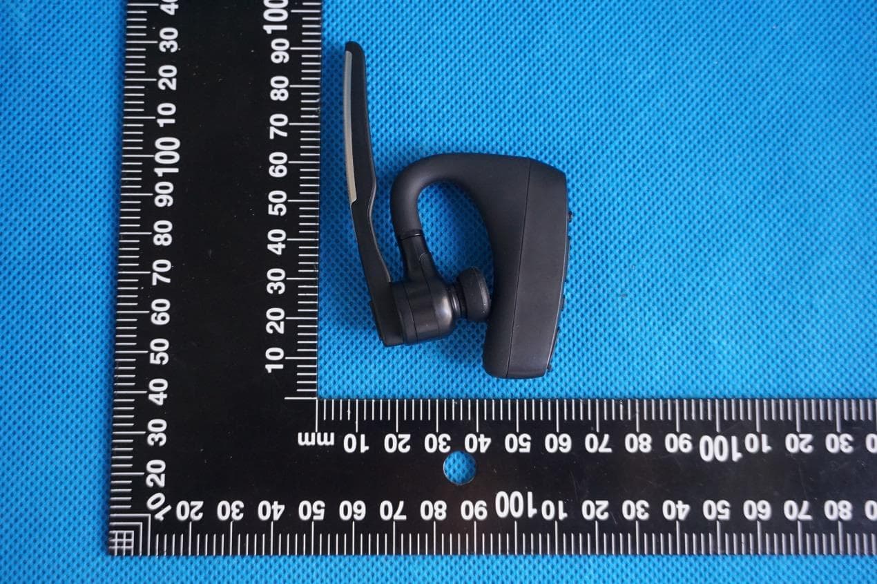
2APZE-K18
Jul 13, 2020Bluetooth headset
Equipment Class
DSS - Part 15 Spread Spectrum Transmitter