2AR3A-ITM-G3IoT Module
Samsung Electronics Co Ltd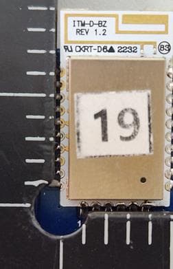
Click to zoom
Application Details
- Equipment Class
- DTS - Digital Transmission System
- Date of Grant
- May 17, 2023
- Application Purpose
- Original Equipment
- Date of Application
- May 17, 2023
- Equipment Note
- IoT Module
- Frequency Range
- 2405.00000000 - 2480.00000000
- Company
- Samsung Electronics Co Ltd
- Country
- South Korea
Documents & Files
Document Text
Text extracted from the exhibit documents filed with the FCC. Open a document above to read the original.
Users Manual
➢ ITM-G3 OEM/Integrators Installation Manual ➢ Confidential Information ➢ Samsung Electronics Co., Ltd. Rev. 1.0 2023. 5. 08 IoT Modul IoT Module ITM-G3 SLP-I211BZXXWW Key Features • ZigBee 3.0 and BLE 5.0 • 4-GPIO channel outputs for Switch control Basic Features Series. Part Number Input Output Connectivity Frequency TX Power ITM-Gen3 SLP-I211BZXXWW 3.3Vdc GPIO ZigBee, BLE 2.4GHz 8dBm • Firmware Version : TBD 1. Specification Article Symbol Specification Unit Note Min. Typ. Max. Electrical SPECIFICATIONS Input Voltage Vin 3.0 3.3 3.8 V Input Current mA 100 mA ENVIRONMENTAL SPECIFICATIONS Operation Temperature -40 85 ºC Storage Temperature -50 150 MECHANICAL SPECIFICATION Dimensions 18.5 x 10.5 x 2.2 mm L x W x H 2. Pin Assignment Pin No. Name Function 1 / 2 / 10 / 14 / 15 / 17 / 18 / 26 GND Ground 3 GPIO1 Light on/Dim up 4 - - 5 GPIO2 Light off/Dim down 6 GPIO3 Status LED 7 GPIO4 LED toggle 8 9 11 Reset Software Reset 12 - - 13 - - 16 Vin Input Voltage 19 20 - - 21 - - 22 - - 23 - - 24 - - 25 - - 3. Dimension 4. Application Guide • Solder PAD • Solder spread area Solder pad shoud be soldered over 60% of full area. • Clearance Area ① Recommend to design a clearance area in the main board for the better performance of antenna radiation. It should be applied to all layers of the board. There shall not be any components, traces, pads or copper areas in any layer within the clearance area. → Minimum clearance area size (non-copper) = 10.5mm x 4.0mm • Reflow Profile Max. Temperature: 245 °C Max. number of reflow cycles: 2 Hand soldering: follow IPC recommendation 5. Label • QR Code Index Contents Digit Product Code SLP-I126BZXXUS 14 Date YYMMDD 6 BT MAC Address AAAA...AAAA 1) 12 ZigBee EUI BBBB...BBBB 2) 16 Install Code CCCC...CCCC 3) 36 Under-Bar _ 4 Total Digit 88 FCC ID QR Code Information: SLP-I211BZXXWW_210928_AAAA...AAAA_BBBB...BBBB_CCCC...CCCC 6. FCC Information This device complies with part 15 of the FCC Results. Operation is subject to the following two conditions: (1) This Device may not cause harmful interface, and (2) This device must accept any interference received, including interference that may cause undesired operation. Note: This equipment has been tested and found to comply with the limits for CLASS B digital device, pursuant to Part 15 of FCC Rules. These limits are designed to provide reasonable protection against harmful interference when the equipment is operated in a commercial environment This equipment generates, uses and can radiate radio frequency energy and, if not installed and used in accordance with the instructions, may cause harmful interference to radio communications. However, there is no guarantee that interference will not occur in a particular installation. If this equipment does cause harmful interference to radio or television reception, which can be determined by turning the equipment off and on, the user is encouraged to try correct the interference by one or more of the following measures: 1.1. Reorient or relocate the receiving antenna. 1.2. Increase the separation between the equipment and receiver. 1.3. Connect the equipment into an outlet on a circuit different from that to which receiver is connected. 1.4. Consult the dealer or experienced radio/TV technician for help. FCC RF Radiation Exposure Statement (1) This Transmitter must not be co-located or operating in conjunction with any other antenna or transmitter. (2) This equipment complies with RF radiation exposure of 20cm between the radiator and your body. WARNING 1. Changes or modifications not expressly approved by the manufacturer could void the user’s authority to operate the equipment. 2. It is necessary to check whether the product using the module meets the certification. 3. Exposure in the finished product should be re-evaluated. CAUTION: Exposure to Radio Frequency Radiation. Antenna shall be mounted in such a manner to minimize the potential for human contact during normal operation. The antenna should not be contacted during operation to avoid the possibility of exceeding the FCC radio frequency exposure limit. 7. Precaution To prevent the module from any defect, please handle and store it with care • Do not drop or give shock • Do not store in very humid location or at extreme temperature • Do not open or disassemble the product Static electricity or surge voltage may damage the components inside the module, as such please observe proper anti- electrostatic working process • People handing the module should be well grounded (e.g. using ESD wrist band) and wear anti-static working clothes and gloves • All related devices and instruments in the production line should be well grounded (e.g. working table, measuring equipment, assembly jigs) Avoid input voltage exceeds the maximum rating, which will cause damage to the circuit and result in malfunction. Specifications are subject to change without notice. RF exposure considerations This modular complies with FCC RF radiation exposure limits set forth for an uncontrolled environment. This transmitter must not be co-located or operating in conjunction with any other antenna or transmitter. RF Exposure - This device is only authorized for use in a mobile application. At least 20 cm of separation distance between the module and the user's body must be maintained at all times. Instruction to Integrator Labelling A label must be affixed to the outside of final commercial product with the following statements: This device contains FCC ID: 2AR3A-ITM-G3 RF exposure considerations Consistent with §2.909(a), the following text must be included within the user’s manual or operator instruction guide for the final commercial product This modular complies with FCC RF radiation exposure limits set forth for an uncontrolledenvironment. This transmitter must not be co-located or operating in conjunction with any other antenna or transmitter. This device is only authorized for use in a mobile application. At least 20 cm of separation distan…
Text truncated - open the document above for the full version.
Attestation Statements
Samsung Electronics Co., Ltd. FCC Attestation Statement US Agent For Service Federal Communications Commission Authorization and Evaluation Division 7435 Oakland Mills Road Columbia, MD 21046 Date: 2023. 04. 18 Ref: Attestation Statements Part 2.911(d)(7) Filing FCC Application for FCC ID: 2AR3A-ITM-G3 Samsung Electronics Co Ltd certifies that, as of the date of the filing of the application, [Jenni Chun] is our designated U.S. agent for service of process for the above reference FCC ID: 2AR3A-ITM-G3. Samsung Electronics Co Ltd agrees to maintain an agent for no less than one year after the grantee has terminated all marketing and importation or the conclusion of any Commission-related proceedings involving the equipment. [Jenni Chun] accepts, as of the date of the filing of the application, the obligation of the designated U.S. agent for service of process for above referenced FCC ID. Designated U.S. Agent Information: Name : Samsung Electronics Co Ltd Address : 19 Chapin Rd., Building D, Pine Brook, NJ07058 Contact Person: Jenni Chun Telephone: 1-800-726-7864 Email : [email protected] FRN : 0005810205 Sincerely, Applicant’s Signature: Agent’s Signature: Applicant’s Name: Moungjin Jang Agent’s Name: Jenni Chun
Attestation Statements
Samsung Electronics Co., Ltd. Attestation Statement Letter I Federal Communications Commission Authorization and Evaluation Division 7435 Oakland Mills Road Columbia, MD 21046 Date: 2023. 04. 18 Ref: Attestation Statements Part 2.911(d)(5)(i) Filing FCC Application for FCC ID: 2AR3A-ITM-G3 Samsung Electronics Co., Ltd. certifies that the equipment for which authorization is sought is not “covered” equipment prohibited for receiving an equipment authorization pursuant to section 2.903 of the FCC rules. Sincerely, Applicant’s Signature: Applicant’s Name: Moungjin Jang
Attestation Statements
Samsung Electronics Co., Ltd. Attestation Statement Letter II Federal Communications Commission Authorization and Evaluation Division 7435 Oakland Mills Road Columbia, MD 21046 USA Date: 2023. 04. 18 Ref: Attestation Statements Part 2.911(d)(5)(ii) Filing FCC Application for FCC ID: 2AR3A-ITM-G3 Samsung Electronics Co., Ltd. certifies that, as of the date of the filing of the application, the applicant is not identified on the Covered List as an entity producing “covered” equipment. Sincerely, Applicant’s Signature: Applicant’s Name: Moungjin Jang
Cover Letter(s)
Date: 04/17/2018 VCB_F-01: Operating Procedures Form – FCC Authorization v02 Page 1 of 1 Samsung Electronics Co., Ltd. Federal Communications Commission Authorization and Evaluation Division 1435 Oakland Mills Road Columbia, MD 21046 Date: 2023. 04. 18 SUBJECT: FCC Application for (FCC ID: 2AR3A-ITM-G3) To Whom It May Concern: We, the undersigned, hereby authorize Eun Hye Gwak of ICR Co.,Ltd on our behalf, to apply to the Federal Communications Commission on our equipment. Any and all acts carried out by ICR Co.,Ltd on our behalf shall have the same effect as acts of our own. This is to advise that we are in full compliance with the Anti- Drug Abuse Act. We, the applicant, are not subject to a denial of federal benefits pursuant to Section 5301 of the Anti-Drug Act of 1988, 21 USC853a, and no party to the application is subject to a denial of federal benefits pursuant to that section. Sincerely, (Must be signed by the person that is listed on the FCC Website) Client’s signature: Client’s name & title: Moungjin Jang / Staff Engineer Contact information / address: Samsung Electronics Co., Ltd. / 1, Samsung-ro, Giheung-gu, Yongin-si Gyeonggi-do, South Korea
Cover Letter(s)
(Samsung Electronics Co., Ltd.) Date: 04/17/2018 VCB_F-01: Operating Procedures Form – FCC Modular v02 Page 1 of 1 MODULAR APPROVAL LETTER (ITM-Gen3) FCC ID : 2AR3A-ITM-G3, is seeking FCC Authorization as a Single Modular transmitter / Single Limited Modular Approval (Please check one) The EUT meets the requirements for Single Modular approval / Single Limited Modular Approval (please check one) as detailed in KDB 996369. Compliance to each of the requirements is described below: Modular Approval Requirement Yes No Please provide a detailed explanation if the answer is “No.” (i) The radio elements of the modular transmitter must have their own shielding. The physical crystal and tuning capacitors may be located external to the shielded radio elements. X (ii) The modular transmitter must have buffered modulation/data inputs (if such inputs are provided) to ensure that the module will comply with part 15 requirements under conditions of excessive data rates or over-modulation. X (iii) The modular transmitter must have its own power supply regulation. X (iv) The modular transmitter must comply with the antenna and transmission system requirements of §§ 15.203, 15.204(b) and 15.204(c). The antenna must either be permanently attached or employ a ‘‘unique’’ antenna coupler (at all connections between the module and the antenna, including the cable). The ‘‘professional installation’’ provision of § 15.203 is not applicable to modules but can apply to limited modular approvals under paragraph (b) of this section. X (v) The modular transmitter must be tested in a stand-alone configuration X (vi) The modular transmitter must be equipped with either a permanently affixed label or must be capable of electronically displaying its FCC identification number. X (vii) The modular transmitter must comply with any specific rules or operating requirements that ordinarily apply to a complete transmitter and the manufacturer must provide adequate instructions along with the module to explain any such requirements. A copy of these instructions must be included in the application for equipment authorization. X (viii) The modular transmitter must comply with any applicable RF exposure requirements in its final configuration. X Client’s signature: Client’s name & title: Moungjin Jang / Staff Engineer Contact information / address: +82-70-7142-1361 / 1, Samsung-ro, Giheung-gu, Yongin-si Gyeonggi-do, South Korea
Cover Letter(s)
Date: 04/17/2018 VCB_F-01: Operating Procedures Form – FCC Confidentiality v03 Page 1 of 1 Samsung Electronics Co., Ltd. Federal Communications Commission Authorization and Evaluation Division Confidentiality Request regarding application for certification of FCC ID: 2AR3A-ITM-G3 Pursuant to Sections 0.457 and 0.459 of the Commission’s Rules, we hereby request confidential treatment of information accompanying this application as outlined below: Type of Confidentiality Requested Exhibit Type ☐Short Term ☒Permanent Block Diagrams ☒Short Term External Photos ☒Short Term ☐Permanent* Internal Photos ☐Short Term ☒Permanent Operation Description ☐Short Term ☒Permanent Parts List/BOM ☐Short Term ☒Permanent Schematics ☒Short Term Test Setup Photos ☒Short Term ☐Permanent* User manual *Requires further justification before permanent confidentiality will be allowed. The above materials contain trade secrets and proprietary information not customarily released to the public. The public disclosure of these materials may be harmful to the applicant and provide unjustified benefits to its competitors. Permanent Confidentiality: The applicant requests the exhibits listed above as permanently confidential be withheld from public review due to materials that contain trade secrets and proprietary information not customarily released to the public. Short-Term Confidentiality: Pursuant to DA04-1705 June 15, 2004 of the Commission’s public notice, we also request temporary confidential treatment of information accompanying this application as outlined below for an initial period of 180(ie- “45”, “90” or “180”) days. Client’s signature: Client’s name & title: Moungjin Jang / Staff Engineer Contact information / address: Samsung Electronics Co., Ltd. / 1, Samsung-ro, Giheung-gu, Yongin-si Gyeonggi-do, South Korea
External Photos
Exterior Photographs Front Top Rear Bottom
ID Label/Location Info
IDENTIFICATION LABEL PROPOSED FCC ID LABEL The FCC ID shall be permanently affixed in the rear side of the equipment FCC ID : 2AR3A-ITM-G3
Internal Photos
Interior Photographs Interior Main Board - Front Top Main Board(Open Shield) - Front Top Main board - Rear Bottom PCB Antenna
RF Exposure Info
페이지(page) : ( 2 )/( 총(Total) 7 ) ICRT-QPA-17-03 Rev.2 Report No. ICRT-TR-E230864-0A Contents 1. Applicant & Manufacturer & Test Laboratory Information .................................................................................. 3 1.1 Applicant information ........................................................................................................................................ 3 1.2 Manufacturer Information ................................................................................................................................. 3 1.3 Test Laboratory Information ............................................................................................................................ 3 2. Equipment under Test(EUT) Information ................................................................................................................. 4 2.1 General Information ........................................................................................................................................... 4 2.2 Additional Information ...................................................................................................................................... 4 2.3 Mode of operation during the test .................................................................................................................. 4 2.4 Modifications of EUT ......................................................................................................................................... 4 3. Maximum Permissible Exposure ............................................................................................................................... 5 3.1 RF Exposure calculation .................................................................................................................................. 5 3.2 Result ..................................................................................................................................................................... 6 3.3 Conclusion of Simultaneous Transmitter .................................................................................................... 7 Revision History Issued Report No. Issued Date Revisions Effect Section ICRT-TR-E230864-0A 2023.04.18 Initial Issue All 페이지(page) : ( 3 )/( 총(Total) 7 ) ICRT-QPA-17-03 Rev.2 Report No. ICRT-TR-E230864-0A 1. Applicant & Manufacturer & Test Laboratory Information 1.1 Applicant information Applicant Samsung Electronics Co., Ltd. Address 1, Samsung-ro, Giheung-gu, Yongin-si Gyeonggi-do, South Korea Contact Person Moungjin Jang Telephone No. +82-70-7142-1361 Fax No. +82-31-8000-8000 E-mail [email protected] 1.2 Manufacturer Information Manufacturer Samsung Electronics Co., Ltd. Address 1, Samsung-ro, Giheung-gu, Yongin-si Gyeonggi-do, South Korea 1.3 Test Laboratory Information Conducted tests were performed at Laboratory ICR Co., Ltd. Address 112, Hwanggeum 3-ro 7beon-gil, Hagun-ri, Yangchon-eup, Gimpo-si, Gyeonggi-do, Korea Telephone No. +82-2-6351-9002 Fax No. +82-2-6351-9007 RRA No. KR0165 KOLAS No. KT652 페이지(page) : ( 4 )/( 총(Total) 7 ) ICRT-QPA-17-03 Rev.2 Report No. ICRT-TR-E230864-0A 2. Equipment under Test(EUT) Information 2.1 General Information Product Name IoT Module Brand Name - Model Name ITM-Gen3 Additional Model Name - FCC ID 2AR3A-ITM-G3 Power Supply DC 3.3 V 2.2 Additional Information Equipment Class DTS-Digital Transmission System Device Type Stand-alone Operating Frequency Bluetooth LE (1/2 Mbps) 2 402 ㎒ ~ 2 480 ㎒ Zigbee 2 405 ㎒ ~ 2 480 ㎒ RF Output Power Bluetooth LE 1 Mbps 7.63 ㏈m Bluetooth LE 2 Mbps 7.66 ㏈m Zigbee 6.28 ㏈m Number of Channel Bluetooth LE (1/2 Mbps) 40 Zigbee 16 Modulation Type Bluetooth LE (1/2 Mbps) GFSK Zigbee O-QPSK Antenna Type PCB Antenna Antenna Gain -1.98 ㏈i Antenna Operating Mode Single antenna exists for each mode 2.3 Mode of operation during the test - The EUT is continuous transmission mode during the test with set at Low Channel, Middle Channel, and High Channel. To get a maximum radiated emission levels from the EUT, the EUT was moved throughout the XY, YZ, XZ planes. 2.4 Modifications of EUT - None 페이지(page) : ( 5 )/( 총(Total) 7 ) ICRT-QPA-17-03 Rev.2 Report No. ICRT-TR-E230864-0A 3. Maximum Permissible Exposure 3.1 RF Exposure calculation According to the FCC rule §1.1310 the limit for General Population/Uncontrolled exposure is 1 ㎽/㎠ for the device operating 1 500 ㎒ ~ 100 000 ㎒. The electric field generated for a 1 ㎽/㎝² exposure is calculated as follows: E = √ (30 * P * G) / D, and S = E² / Z = E² / 377, because 1 ㎽/㎝² = 10 W/m² S = Power density in ㎽/㎝², Z = Impedance of free space, 377 Ω P = Power input to the external antenna (Output power from the EUT antenna port (㏈m) – cable loss (㏈)), E = Electric filed strength in V/m, G = Numeric antenna gain, and D = distance in meter Combing equations and rearranging the terms to express the distance as a function of the remaining variable D = √ (30 * P * G) / (377 *10 S) Changing to units of ㎽ and cm, using P (㎽) = P (W) / 1 000, d (㎝) = 0.01 * d (m) D = 0.282 * √ (P * G) / S 페이지(page) : ( 6 )/( 총(Total) 7 ) ICRT-QPA-17-03 Rev.2 Report No. ICRT-TR-E230864-0A 3.2 Result According to above equation, the following result was obtained. Operating Mode Target Power W / tolerance Max tune up power Antenna Gain Safe Distance (㎝) Power Density (㎽/㎝²) @ 20 ㎝ Separation Limit (㎽/㎝²) (㏈m) (㎽) Log Linear Zigbee 6.28. ± 1.0 7.28 5.35 -1.98 0.63 0.52 0.000 67 1.00 Blutooth LE 1 Mbps 7.63. ± 1.0 8.63 7.29 0.61 0.000 92 Blutooth LE 2 Mbps 7.66 ± 1.0 8.66 7.35 0.61 0.000 93 According to above table, for Band(Zigbee), safe distance, D = 0.282 * √ (7.35 * 0.63)/1.00 = 0.61 ㎝. For getting power density at 20 ㎝ separation in above table, following formula was used. S = P * G / (4π * R²) = (7.35 * 0.63 / (4 * π * 20 2 ) = 0.000 93 페이지(page) : ( 7 )/( 총(Total) 7 ) ICRT-QPA-17-03 Rev.2 Report No. ICRT-TR-E230864-0A 3.3 Conclusion of Simultaneous Transmitter Operating Freq. Band Ope…
Text truncated - open the document above for the full version.
Test Report
NO. Version 1.0 Antenna Specification Model I T M - G e n 3 Model Number SLP-I211BZXXWW ITM specification PRODUCT NAME ITM-Gen3 MODEL CODE SLP-I211BZXXWW APPLIED MODEL JC Controller PRODUCT SPECIFICATION BLE, ZigBee [ Information ] This is an IOT module that controls lighting using BLE +Zigbee. I. Supports BLE +Zigbee II . It consists of a built -in antenna(PCB ) III . It controls external LED instead of wall switch ANTENNA Electrical characteristics I. Operating frequency band - BT ANTENNA Band Frequency [MHz ] BLUETOOTH 2400 2485 II . Electrical specifications - The antenna must meet the requirements specified in the electrical specifications. Impedance 50 Ω Partiality Linear Radiation pattern Omni directional Maximum output 100 mWatte MANUFACTURER ADRESS 6 RFtech MANUFACTURER 0, Jukyang-daero 1763beon-gil, Wonsam-myeon, Cheoin-gu, Yongin-si, Gyeonggi-do, Korea Measurement method I.VSWR and SMITH CHART 1-1. Power on Network Analyzer. 1-2. Set the start frequency and end frequency for optimal calibration. 1-3. Perform One port calibration in the order of open , short , load and check for abnormalities. 1-4. Since the characteristics of the antenna are greatly affected by surrounding metal objects,avoid from Network Analyzer. -. Condition Electrical Characteristics DATA I.Matching Values ANTENNA Matching Value B/T TEST POINT II.VSWR Band Bluetooth 2400MHz 2442.5MHz 2485MHz VSWR 2.4 : 1 less 1.4 : 1 less 1.4 : 1 less I.Smith chart ANTENNASMITH CHART B/T ANTENNAVSWR B/T GAIN DATA / RADIATION PATTERN I.3D Gain/Radiation pattern measurement mathod II.Chamber setup and calibration . Install the standard gain horn antenna suitable for the frequency to be measured toward the reflector. . Frequency setting and calibration III.Antenna measurement procedure . Connect the cable to the port on the antenna and measure the radiation pattern using a measurement program . Setting the measurement frequency and measuring horizontal and vertical radiation pattern. . Save the raw data after checking the measurement result. IV.Equipment Classfication Description Specificatons Remark Test site No reflection Passive Chamber 3m x 2.5m x 3m - Equipment Network Analyzer Keysight E5071B - PC(Desktop) I3-3220 / 8GB - V.Peak Gain . The gain of the antenna is displayed in [dBi] by setting the horn antenna to the standard antenna Frequency Range Bluetooth 2400MHz 2450MHz 2500MHz Peak. Gain H -3.90 -2.23 -3.32 E1 -4.01 -1.98 -2.68 E2 -4.36 -2.06 -2.40 I.1.1ANTENNA (1)H Plane (2)E1 Plane FrequencyAvg. GainEfficiency [MHz]Θ [Deg]Φ[Deg] Value[dBi] Θ [Deg]Φ[Deg] Value[dBi][dBi][%] 1240090255-3.909015-8.34-5.5128.13 2242590255-4.279015-8.41-5.6427.32 324509090-2.239015-6.07-3.4045.68 42475902700.159015-3.12-0.7683.92 5250090270-3.329015-6.37-4.2837.31 No Maximum ValueMinimum Value H Plane (Vertical + Horizontal) Polar Chart -9 -8 -7 -6 -5 -4 -3 -2 -1 0 1 0 15 30 45 60 75 90 105 120 135 150 165 180 195 210 225 240 255 270 285 300 315 330 345 2400 2425 2450 2475 2500 FrequencyAvg. GainEfficiency [MHz]Θ [Deg]Φ[Deg] Value[dBi] Θ [Deg]Φ[Deg] Value[dBi][dBi][%] 1240090-90-4.0190-150-22.70-6.9919.98 2242590120-4.3090-150-24.55-7.2019.06 3245090-105-1.9890-150-23.21-4.9831.75 4247590-1050.7290-150-19.30-2.3658.06 5250090-105-2.6890-150-24.78-5.9025.71 No Maximum ValueMinimum Value E1 Plane (Vertical + Horizontal) Polar Chart -25 -20 -15 -10 -5 0 5 0 15 30 45 60 75 90 105 120 135 150 165 180 -165 -150 -135 -120 -105 -90 -75 -60 -45 -30 -15 2400 2425 2450 2475 2500 (3) E2 Plane FrequencyAvg. GainEfficiency [MHz]Θ [Deg] Φ[Deg] Value[dBi] Θ [Deg] Φ[Deg] Value[dBi][dBi][%] 1240090-135-4.3690-150-25.10-8.5913.82 2242590-135-4.3690-150-25.22-8.8113.15 3245090-120-2.0690-150-25.43-6.6421.66 4247590-1200.8190-150-22.20-3.9640.21 5250090-120-2.4090-150-26.72-7.3418.43 No Maximum ValueMinimum Value E2 Plane (Vertical + Horizontal) Polar Chart -30 -25 -20 -15 -10 -5 0 5 0 15 30 45 60 75 90 105 120 135 150 165 180 -165 -150 -135 -120 -105 -90 -75 -60 -45 -30 -15 2400 2425 2450 2475 2500
Test Report
페이지(page) : ( 2 )/( 총(Total) 60 ) ICRT-QPA-17-03 Rev.2 Report No. ICRT-TR-E230863-0A Contents 1. Applicant & Manufacturer & Test Laboratory Information .................................................................................. 4 1.1 Applicant information ........................................................................................................................................ 4 1.2 Manufacturer Information ................................................................................................................................. 4 1.3 Test Laboratory Information ............................................................................................................................ 4 2. Equipment under Test(EUT) Information ................................................................................................................. 5 2.1 General Information ........................................................................................................................................... 5 2.2 Additional Information ...................................................................................................................................... 5 2.3 Mode of operation during the test .................................................................................................................. 5 2.4 Modifications of EUT ......................................................................................................................................... 5 3. Test Summary ................................................................................................................................................................. 6 3.1 Test standards and results .............................................................................................................................. 6 3.2 Purpose of the test ............................................................................................................................................. 6 3.3 Test Methodology ............................................................................................................................................... 6 3.4 Configuration of Test System ......................................................................................................................... 6 3.5 Antenna requirement ......................................................................................................................................... 7 4. Used equipment on test ............................................................................................................................................... 8 5. 6 ㏈ Bandwidth .............................................................................................................................................................. 9 5.1 Operating environment ..................................................................................................................................... 9 5.2 Measurement method ........................................................................................................................................ 9 5.3 Test data ............................................................................................................................................................... 9 6. Maximum Conducted Output Power ....................................................................................................................... 16 6.1 Operating environment ................................................................................................................................... 16 6.2 Measurement method ...................................................................................................................................... 16 6.3 Test data ............................................................................................................................................................. 16 7. Power Spectral Density .............................................................................................................................................. 23 7.3 Operating environment ................................................................................................................................... 23 7.4 Measurement method ...................................................................................................................................... 23 7.5 Test data ............................................................................................................................................................. 23 8. Conducted Spurious Emission ................................................................................................................................ 30 8.3 Operating environment ................................................................................................................................... 30 8.4 Measurement method ...................................................................................................................................... 30 8.5 Test data ............................................................................................................................................................. 30 9. Radiated Spurious Emission .................................................................................................................................... 45 9.3 Operating environment ................................................................................................................................... 45 9.4 Measurement method ...................................................................................................................................... 45 9.5 Test setup .......................................................…
Text truncated - open the document above for the full version.
Contact Information
Applicant
Moungjin Jang(Staff Engineer)
Test Firm
ICR Co., Ltd.Sim Sang-Woo
Technical Specifications
| # | Rule Parts | Frequency Range | Power Output |
|---|---|---|---|
| 2 | 15C | 2.40 GHz - 2.48 GHz | 4.25 mW |