2ASEO-HPYKE242.4G&5G Dual Band WIFI Module
Shenzhen HOPE Microelectronics Co., Ltd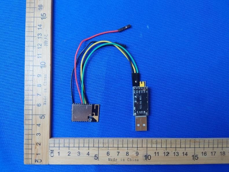
Click to zoom
Application Details
- Equipment Class
- DTS - Digital Transmission System
- Date of Grant
- Sep 25, 2024
- Application Purpose
- Original Equipment
- Date of Application
- Sep 25, 2024
- Equipment Note
- 2.4G&5G Dual Band WIFI Module
- Frequency Range
- 2412.00000000 - 2462.00000000
- Country
- China
Documents & Files
Document Text
Text extracted from the exhibit documents filed with the FCC. Open a document above to read the original.
Users Manual
1 / 14 HPYKE24 V1.0 Dual-Band WIFI Module HPYKE24 Datasheet 2 / 14 HPYKE24 V1.0 1. Product Overview: HPYKE24 is a dual-band Wi-Fi module developed by ShenZhen Hope Microelectronics based on the RTL8720DN. It supports dual-band WLAN (2.4GHz and 5GHz). The module integrates high-performance ARM V8 (Cortex-M4F compatible) and low-power ARM V8M (Cortex-M0 compatible) microcontrollers, WLAN (802.11 a/b/g/n), MAC, and RF baseband. It also provides multiple configurable GPIOs for controlling different peripheral devices. Figure 1. System architecture Key Features: - Supports 802.11a/b/g/n, 2.4GHz or 5GHz. - Supports HT20/HT40 modes. - Includes low-power beacon monitoring, receiving, and suspend modes. - Built-in AES/DES/SHA hardware engines. - Supports TrustZone-M and secure boot. - Supports SWD debugging port protection. - Supports STA/AP/STA+AP operation modes. - Provides one-click network setup for Android/iOS using the Simple Config App. - Local and remote firmware updates supported (FOTA). - Programmable in Linux and Windows environments, and also supports Arduino development. 3 / 14 HPYKE24 V1.0 Module parameters Table 1. Module parameters Model HPYKE24 Package SMD-18.8 Dimensions 28*18.8*3(±0.2)MM Antenna PCB onboard or IPEX antenna Frequency Range 2400-2483.5MHz (2.4GHz) or 5180-5825MHz (5GHz) Frequency Range 2.402GHz - 2.480GHz Operating Temperature -40 °C ~ 85 °C Storage Conditions -40 °C ~ 125 °C , < 90%RH Power Supply 3.0V ~ 3.6V,typical 3.3V,current >500mA Peripherals UART/GPIO/ADC/PWM/IIC/SPI/SWD Certification RoHS, FCC FLASH 16Mbit by default (supports 32Mbit, 64Mbit and 128Mbit options) 4 / 14 HPYKE24 V1.0 2. Electrical Characteristics Table 2. Electrical Characteristics Parameter Min. Typ. Max. Unit Supply Voltage 3.0 3.3 3.6 V Digital I/O supply voltage 1.76 1.8-3.3 3.3 mA I/O Rating current 50 mA Table 3. ESD Characteristics Reliability Test Standards Test condition Result Human Body Model (HBM) JEDEC EIA / JESD22-A114 ±2000V Pass Charge Device Model (CDM) JEDEC EIA / JESD22-C101 ±500V Pass Note: The HPYKE24 module is sensitive to electrostatic discharge (ESD). Special precautions should be taken, such as adding ESD protection devices during use. 3. Radio Characteristics Table 4. Radio Characteristics Description Typ. Unit Frequency Range 2400-2483.5 or 5180-5825 MHz Output power 802.11a mode, PA output 14±2 dBm 802.11n mode, PA output 14±2 dBm 802.11g mode, PA output 15±2 dBm 802.11b mode, PA output 16±2 dBm Rx Sensitivity CCK, 1 Mbps <=-90 dBm CCK, 11 Mbps <=-85 dBm 6 Mbps (1/2 BPSK) <=-88 dBm 5 / 14 HPYKE24 V1.0 54 Mbps (3/4 64-QAM) <=-70 dBm 4. Dimension Figure 2. Module Dimension 6 / 14 HPYKE24 V1.0 5. Pin Definition The HPYKE24 module has 16 pins with different functions such as power supply, UART communication, and GPIO interfaces. The figure below illustrates the pin definition. Figure 3. Pin definition (Bottom view) Table 2. Module pin definition Pin Name Description 1 PA13 LP_PWM1/SPI1_MISO 2 PB3 ADC/SWD_CLK 3 CHIP_EN Enable pin, pull-up to enable the module 4 PA15 SPI1_CS 5 PA8 UART_LOG_RXD, RX port for firmware programming and command input. 6 PA27 SWD_DATA 7 PA26 LP_I2C_SDA/LP_PWM5 8 VDD_3V3 3.3V Power supply (VDD) 9 GND Ground 10 PA25 LP_I2C_SCL/LP_PWM4 11 PA7 UART_LOG_TXD, TX port for firmware programming and log output 12 PA14 SPI1_CLK 13 PA30 LP_PWM1 14 PA12 SPI1_MOSI/LP_PWM0 7 / 14 HPYKE24 V1.0 15 PB2 LP_UART_RXD, RX port for the AT command interface 16 PB1 LP_UART_TXD, TX port for the AT command interface 8 / 14 6. Design Guidelines 6.1 Reference circuit design of the HPYKE24 module. Figure 4. Reference schematic 6.2 Recommended module packaging design dimensions Figure 5. Module package 6.3 PCB Layout and Placement 9 / 14 For optimal performance of the WiFi module Option 1: Place the module aligned to the edge of the application PCB or leave the antenna area out of the application PCB, as illustrated in the figures below. Option 2: Leave the antenna clearance area void of any traces, components, or copper on all layers of the application PCB if you are going to use the on-board chip antenna Note: Do not place plastic or any other dielectric material in contact with the antenna. Figure 6. Recommended Layout 6.4 Power Supply Recommend 3.3V voltage with a current supply above 500mA. It is suggested to use an LDO for power supply; if a DC-DC design is used, it is recommended to control the ripple within 30mV. It is advised to reserve space for a dynamic response capacitor in the DC-DC power supply circuit to optimize output ripple during large load changes. It is recommended to add ESD protection devices to the 3.3V power supply interface. 10 / 14 6.5 GPIO Pins The HPYKE24 includes some GPIO ports and it is recommended to connect a 10-100 ohm resistor in series with the I/O port. This can suppress overshoot and stabilize the voltage levels on both sides. It also helps with EMI and ESD protection. For special I/O ports with pull-up or pull-down configurations, refer to the usage instructions in the specification. This can affect the module's startup configuration. The module's I/O ports operate at 3.3V. If the main controller's I/O voltage level does not match the module, a level-shifting circuit will be needed. If the I/O ports are directly connected to peripheral interfaces or pins, it is recommended to reserve space for ESD protection devices near the terminals on the I/O traces. Figure 7. Voltage level-shifting circuit 11 / 14 7. Soldering Recommendations It is recommended that final PCB assembly of the HPYKE24 module follows the industry standard as identified by the Institute for Printed Circuits (IPC). Sometimes a PCB must be reflowed multiple times based on the nature of the design and components used or limitations of the assembly line. During a single reflow cycle, every component is exposed to and stressed with high temperature. Exposing parts to high temperature for multiple times can damage the parts. It is always recommended to avoid more than two…
Text truncated - open the document above for the full version.
Attestation Statements
Attestation Statements 9/23/2024 TO: Federal Communications Commission Authorization and Evaluation Division 7435 Oakland Mills Road Columbia, MD 21046, USA RE: Attestation Statements Part 2.911(d)(7) request for 2ASEO-HPYKE24 Shenzhen HOPE Microelectronics Co., Ltd the undersigned, hereby authorize THREE STONES MEDIA LLC to act as our designated U.S. agent for service of process, Shenzhen HOPE Microelectronics Co., Ltd accepts to maintain an agent for no less than one year after the grantee has terminated all marketing and importation or the conclusion of any Commission-related proceeding involving the equipment. THREE STONES MEDIA LLC accepts the responsibility to act as designated U.S. agent for service of process. Applicant Information: Company name: Shenzhen HOPE Microelectronics Co., Ltd Contact Name: Daniel Chen Address: 30th floor of 8th Building, C Zone Vanke Cloud City, Xili Sub-district, Nanshan ,Shenzhen, Guangdong, China FRN: 0028180610 Telephone No: +8675582973805 Email: [email protected] Signature [Daniel Chen] U.S. Agent Information: Company Name: THREE STONES MEDIA LLC Address: 1200 Broadway St. APT 329, Los Angeles, CA90015 FRN: 0033401761 Contact Name: Sijie Zhang Telephone No: +1 267 909 3692 Email: [email protected] Signature [Sijie Zhang]
Attestation Statements
Shenzhen HOPE Microelectronics Co., Ltd 2024-09-19 Eurofins Electrical and Electronic Testing NA, Inc. 914 West Patapsco Avenue Baltimore, MD 21230 RE: Attestation Statements Part 2.911(d)(5)(i) request for (FCC ID: 2ASEO-HPYKE24) [Shenzhen HOPE Microelectronics Co., Ltd ] (“the applicant”) certifies that the equipment for which authorization is sought is not “covered” equipment prohibited from receiving an equipment authorization pursuant to section 2.903 of the FCC rules. Sincerely, Daniel Chen Manager Shenzhen HOPE Microelectronics Co., Ltd 30th floor of 8th Building, C Zone Vanke Cloud City, Xili Sub-district, Nanshan, Shenzhen, Guangdong, China Shenzhen HOPE Microelectronics Co., Ltd 2024-09-19 Eurofins Electrical and Electronic Testing NA, Inc. 914 West Patapsco Avenue Baltimore, MD 21230 RE: Attestation Statements Part 2.911(d)(5)(ii) request for(FCC ID: 2ASEO-HPYKE24 ) [Shenzhen HOPE Microelectronics Co., Ltd] (“the applicant”) certifies that, as of the date of the filing of the application, the applicant is not identified on the Covered List as an entity producing “covered” equipment. Sincerely, Daniel Chen Manager Shenzhen HOPE Microelectronics Co., Ltd 30th floor of 8th Building, C Zone Vanke Cloud City, Xili Sub-district, Nanshan, Shenzhen, Guangdong, China
Cover Letter(s)
Shenzhen HOPE Microelectronics Co., Ltd Request for Modular/Limited Modular Approval Date: September 23, 2024 Subject: Manufacturer’s Declaration for ☒ - Modular Approval ☐ - Split Modular Approval ☐ - Limited Modular Approval ☐ - Limited Split Modular Approval Confidentiality Request for: ______2ASEO-HPYKE24______ 8 Basic Requirements – FCC Part 15.212(a)(1) For Items Marked “NO(*)”, the Limited Module Description Must be Filled Out on the Following Pages Modular Approval Requirement Requirement Met 1. The modular transmitter must have its own RF shielding. This is intended to ensure that the module does not have to rely upon the shielding provided by the device into which it is installed in order for all modular transmitter emissions to comply with FCC limits. It is also intended to prevent coupling between the RF circuitry of the module and any wires or circuits in the device into which the module is installed. Such coupling may result in non-compliant operation. The physical crystal and tuning capacitors may be located external to the shielded radio elements. 15.212(a)(1)(i) ☒ - YES ☐ - NO(*) 2. The modular transmitter must have buffered modulation/data inputs (if such inputs are provided) to ensure that the module will comply with FCC requirements under conditions of excessive data rates or over-modulation. 15.212(a)(1)(ii) ☒ - YES ☐ - NO(*) 3. The modular transmitter must have its own power supply regulation on the module. This is intended to ensure that the module will comply with FCC requirements regardless of the design of the power supplying circuitry in the device into which the module is installed. 15.212(a)(1)(iii) ☒ - YES ☐ - NO(*) 4. The modular transmitter must comply with the antenna and transmission system requirements of §§ 15.203, 15.204(b), 15.204(c), 15.212(a), and 2.929(b). The antenna must either be permanently attached or employ a ‘‘unique’’ antenna coupler (at all connections between the module and the antenna, including the cable). The ‘‘professional installation’’ provision of § 15.203 is not applicable to modules but can apply to limited modular approvals under paragraph 15.212(b). 15.212(a)(1)(iv) ☒ - YES ☐ - NO(*) 5. The modular transmitter must be tested in a stand-alone configuration, i.e., the module must not be inside another device during testing. This is intended to demonstrate that the module is capable of complying with Part 15 emission limits regardless of the device into which it is eventually installed. Unless the transmitter module will be battery powered, it must comply with the AC line conducted requirements found in Section 15.207. AC or DC power lines and data input/output lines connected to the module must not contain ferrites, unless they will be marketed with the module (see Section 15.27(a)). The length of these lines shall be length typical of actual use or, if that length is unknown, at least 10 centimeters to insure that there is no coupling between the case of the module and supporting equipment. Any accessories, peripherals, or support equipment connected to the module during testing shall be unmodified or commercially available (see Section 15.31(i)). 15.212(a)(1)(v) ☒ - YES ☐ - NO(*) Shenzhen HOPE Microelectronics Co., Ltd Modular Approval Requirement Requirement Met 6. The modular transmitter must be labeled with its own FCC ID number, or use an electron display (see KDB Publication 784748). If using a permanently affixed label with its own FCC ID number, if the FCC ID is not visible when the module is installed inside another device, then the outside of the device into which the module is installed must also display a label referring to the enclosed module. This exterior label can use wording such as the following: “Contains Transmitter Module FCC ID: XYZMODEL1” or “Contains FCC ID: XYZMODEL1.” Any similar wording that expresses the same meaning may be used. The Grantee may either provide such a label, an example of which must be included in the application for equipment authorization, or, must provide adequate instructions along with the module which explain this requirement. In the latter case, a copy of these instructions must be included in the application for equipment authorization. If the modular transmitter uses an electronic display of the FCC identification number, the information must be readily accessible and visible on the modular transmitter or on the device in which it is installed. If the module is installed inside another device, then the outside of the device into which the module is installed must display a label referring to the enclosed module. This exterior label can use wording such as the following: “Contains FCC certified transmitter module(s).” Any similar wording that expresses the same meaning may be used. The user manual must include instructions on how to access the electronic display. A copy of these instructions must be included in the application for equipment authorization. 15.212(a)(1)(vi) ☒ - YES ☐ - NO(*) 7. The modular transmitter must comply with all specific rule or operating requirements applicable to the transmitter, including all the conditions provided in the integration instructions by the grantee. A copy of these instructions must be included in the application for equipment authorization. For example, there are very strict operational and timing requirements that must be met before a transmitter is authorized for operation under Section 15.231. For instance, data transmission is prohibited, except for operation under Section 15.231(e), in which case there are separate field strength level and timing requirements. Compliance with these requirements must be assured. 15.212(a)(1)(vii) ☒ - YES ☐ - NO(*) 8. The modular transmitter must comply with any applicable RF exposure requirements. For example, FCC Rules in Sections 2.1091, 2.1093 and specific Sections of Part 15, including 15.319(i), 15.407(f), 15.253(f) and 15.255(g), require that Unlicensed PCS, UNII and millimeter wave devices …
Text truncated - open the document above for the full version.
External Photos
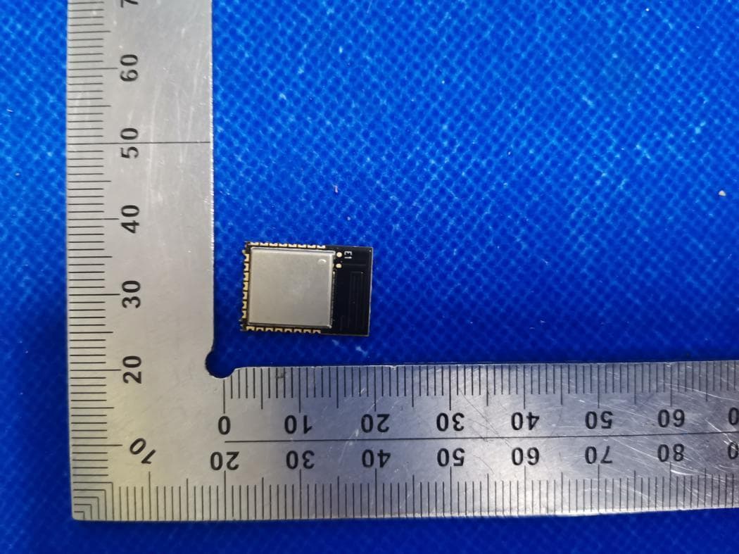
External
ID Label/Location Info
HOPERF Model No: HPYKE24 FCC ID: 2ASEO-HPYKE24
Internal Photos
Internal . 2.4G&5G WIFI Antenna
RF Exposure Info
RF EXPOSURE EVALUATION According to FCC 1.1310: The criteria listed in the following table shall be used to evaluate the environment impact of human exposure to radio frequency(RF) Radiation as specified in ß1.1307(b) FCC ID: 2ASEO-HPYKE24 EUT Specification EUT 2.4G&5G Dual Band WIFI Module Model Number HPYKE24 Input Rating DC 3.3V Frequency band (Operating) BT: 2.402GHz ~ 2.480GHz WLAN: 2.412GHz ~ 2.462GHz WLAN: 5.18GHz ~ 5.32GHz WLAN: 5.745GHz ~ 5825GHz Device category Portable (<20cm separation) Mobile (>20cm separation) Exposure classification Occupational/Controlled exposure (S = 5mW/cm2) General Population/Uncontrolled exposure (S=1mW/cm2) Antenna diversity Single antenna Multiple antennas Tx diversity Rx diversity Tx/Rx diversity Max. output power(peak power ) IEEE 802.11b: 16.39 dBm IEEE 802.11g: 15.26 dBm IEEE 802.11n-HT20: 14.95 dBm IEEE 802.11n-HT40: 14.99 dBm 5180 MHz to 5240 MHz: 14.92 dBm 5745 MHz to 5825 MHz: 14.70 dBm Antenna gain (Max) 2.4GHz WIFI: 1 dBi 5.8G WIFI: 4 dBi Evaluation applied MPE Evaluation SAR Evaluation Limits for Maximum Permissible Exposure(MPE) Frequency Range(MHz) Electric Field Strength(V/m) Magnetic Field Strength(A/m) Power Density(mW/cm 2 ) Average Time (A) Limits for Occupational/Control Exposures 300-1500 -- -- F/300 6 1500-100000 -- -- 5 6 (B) Limits for General Population/Uncontrol Exposures 300-1500 -- -- F/1500 6 1500-100000 -- -- 1 30 Friis transmission formula: Pd=(Pout*G)\(4*pi*R2) Where Pd= Power density in mW/cm 2 , Pout=output power to antenna in Mw G= gain of antenna in linear scale, Pi=3.1416 R= distance between observation point and center of the radiator in cm=20cm Pd the limit of MPE, 1mW/cm2. If we know the maximum gain of the antenna and total power input to the antenna, through the calculation, we will know the distance where the MPE limit is reached. For multiple RF sources: Multiple RF sources are exempt if: in the case of fixed RF sources operating in the same time-averaging period, or of multiple mobile or portable RF sources within a device operating in the same time averaging period, if the sum of the fractional contributions to the applicable thresholds is less than or equal to 1 as indicated in the following equation Evaluated k : the maximum reported SAR or MPE of fixed, mobile, or portable RF source k either in the device or at the transmitter site from an existing evaluation at the location of exposure. Exposure Limit k : either the general population/uncontrolled maximum permissible exposure (MPE) or specific Absorption rate (SAR) limit for each fixed, mobile, or portable RF source k. Measurement Result Operation Mode Channel Frequency (MHz) Max Measured Power (dBm) Tune up tolerance (dBm) Max tune up conducted power (dBm) Output Peak power (mW) Ant. Gain (dBi) Ant. Gain (numeric) Power density at 20cm (mW/ cm2) Power density Limits (mW/ cm2) 2.4GHz WIFI (802.11b) 2462 16.39 16±1 17 50.119 1 1.259 0.012552 1 5180 MHz to 5240MHz (802.11n 40) 5180 14.92 15±1 16 39.811 4 2.512 0.019894 1 5745 MHz to 5825MHz (802.11n 20) 5745 14.70 15±1 16 39.811 4 2.512 0.019894 1 Maximum Simultaneous transmission MPE Ratio for 2.4G WIFI & 5.8G WIFI Maximum MPE ratio (2.4G WIFI) Maximum MPE ratio (5.8G WIFI) ∑ MPE ratios Limit Results 0.012552 0.019894 0.032446 1.000 Pass The Product unsupported at the same time to Transmitting. According to KDB 447498, and no simultaneous SAR measurement is required. Signature: Shawn Wen Date: 2024-09-10
Test Report
PCBWiFiAntenna Features Widebandwidth RoHScompliant Applications Dual-band2.4/5.5GHzWLAN Specifications Type FrequencyRange (MHz) PeakGain (dBityp.) AverageGain (dBityp.) VSWR Impedance PCB Antenna 2400~2480 1.0(XZ-Total) -3.5(XZ-Total) 6.5max. 50 5150~5850 4.0(XZ-Total) -2.5(XZ-Total) 4.5max. 50 Dimensions Unit:mm Mark L W T Dimensions 0.1 6.90.1 0.8max ReturnLoss(withmatching) 7 6 5 4 3 m139 m146 2 m140 m149 m147 1 0 2.0 m148 2.5 3.0 3.5 4.0 4.5 5.0 5.5 freq,GHz 6.0 freq(2.000GHzto6.000GHz) m139 freq=2.400GHz VSWR=2.919 m140 freq=2.442GHz VSWR=1.498 m146 freq=2.484GHz VSWR=1.944 m149 freq=5.150GHz VSWR=1.664 m148 freq=5.500GHz VSWR=1.124 m147 freq=5.850GHz VSWR=1.876 m150 m151 m151 freq=5.500GHz S(1,1)=0.059 / 59.150 impedance = 52.817 + j5.324 m150 freq=2.442GHz S(1,1)=0.199 / 110.889 impedance = 40.626 + j15.755 VSWR S(1,1) XZ-plane @2440MHz Total YZ-plane @2440MHz Total [email protected] (AntennaEfficiency42%@2.4GHz;60%@2.44GHz;56%@2.48GHz) Y:Φ(Phi)=90 o X:Φ(Phi)=0 o Z : θ(Theta)=0 o XY-plane @2440MHz Total XZ-plane @5500MHz Total YZ-plane @5500MHz Total [email protected] (AntennaEfficiency78%@5.15GHz;86%@5.5GHz;76%@5.85GHz) Y:Φ(Phi)=90 o X:Φ(Phi)=0 o Z : θ(Theta)=0 o XY-plane @5500MHz Total
Test Report
1 / 38 Appendix B Duty Cycle Condition Mode Frequency (MHz) Antenna On Time (ms) Period (ms) Duty Cycle (%) Correction Factor (dB) 1/T (kHz) Final settingFor VBW (kHz) NVNT b 2412 Ant1 12.42 12.55 98.96 0 0.08 1 NVNT b 2437 Ant1 12.42 12.55 98.96 0 0.08 1 NVNT b 2462 Ant1 12.42 12.55 98.96 0 0.08 1 NVNT g 2412 Ant1 2.06 2.19 94.06 0.27 0.48 1 NVNT g 2437 Ant1 2.06 2.19 94.06 0.27 0.48 1 NVNT g 2462 Ant1 2.06 2.19 94.06 0.27 0.48 1 NVNT n20 2412 Ant1 1.92 2.05 93.66 0.28 0.52 1 NVNT n20 2437 Ant1 1.92 2.05 93.66 0.28 0.52 1 NVNT n20 2462 Ant1 1.92 2.05 93.66 0.28 0.52 1 NVNT n40 2422 Ant1 0.94 1.07 87.85 0.56 1.06 1 NVNT n40 2437 Ant1 0.94 1.07 87.85 0.56 1.06 1 NVNT n40 2452 Ant1 0.95 1.07 88.79 0.52 1.06 1 2 / 38 Maximum Conducted Output Power Condition Mode Frequency (MHz) Antenna Conducted Power (dBm) Duty Factor (dB) Total Power (dBm) Limit (dBm) Verdict NVNT b 2412 Ant1 14.78 0 16.21 30 Pass NVNT b 2437 Ant1 15.25 0 16.25 30 Pass NVNT b 2462 Ant1 15.39 0 16.39 30 Pass NVNT g 2412 Ant1 14.26 0 15.26 30 Pass NVNT g 2437 Ant1 15 0 15 30 Pass NVNT g 2462 Ant1 14.95 0 15.15 30 Pass NVNT n20 2412 Ant1 14.48 0 14.48 30 Pass NVNT n20 2437 Ant1 14.95 0 14.95 30 Pass NVNT n20 2462 Ant1 14.7 0 14.7 30 Pass NVNT n40 2422 Ant1 14.99 0 14.99 30 Pass NVNT n40 2437 Ant1 14.94 0 14.94 30 Pass NVNT n40 2452 Ant1 14.98 0 14.98 30 Pass 3 / 38 -6dB Bandwidth Condition Mode Frequency (MHz) Antenna -6 dB Bandwidth (MHz) Limit -6 dB Bandwidth (MHz) Verdict NVNT b 2412 Ant1 8.07 0.5 Pass NVNT b 2437 Ant1 7.8 0.5 Pass NVNT b 2462 Ant1 8.55 0.5 Pass NVNT g 2412 Ant1 16.32 0.5 Pass NVNT g 2437 Ant1 16.35 0.5 Pass NVNT g 2462 Ant1 16.29 0.5 Pass NVNT n20 2412 Ant1 17.04 0.5 Pass NVNT n20 2437 Ant1 16.56 0.5 Pass NVNT n20 2462 Ant1 16.32 0.5 Pass NVNT n40 2422 Ant1 35.04 0.5 Pass NVNT n40 2437 Ant1 33.48 0.5 Pass NVNT n40 2452 Ant1 33.84 0.5 Pass 4 / 38 Test Graphs -6dB Bandwidth NVNT b 2412MHz Ant1 -6dB Bandwidth NVNT b 2437MHz Ant1 5 / 38 -6dB Bandwidth NVNT b 2462MHz Ant1 -6dB Bandwidth NVNT g 2412MHz Ant1 6 / 38 -6dB Bandwidth NVNT g 2437MHz Ant1 -6dB Bandwidth NVNT g 2462MHz Ant1 7 / 38 -6dB Bandwidth NVNT n20 2412MHz Ant1 -6dB Bandwidth NVNT n20 2437MHz Ant1 8 / 38 -6dB Bandwidth NVNT n20 2462MHz Ant1 -6dB Bandwidth NVNT n40 2422MHz Ant1 9 / 38 -6dB Bandwidth NVNT n40 2437MHz Ant1 -6dB Bandwidth NVNT n40 2452MHz Ant1 10 / 38 Maximum Power Spectral Density Level Condition Mode Frequency (MHz) Antenna Conducted PSD (dBm/3kHz) Duty Factor (dB) Total PSD (dBm/3kHz) Limit (dBm/3kHz) Verdict NVNT b 2412 Ant1 -11.91 0 -11.91 8 Pass NVNT b 2437 Ant1 -10.98 0 -10.98 8 Pass NVNT b 2462 Ant1 -10.74 0 -10.74 8 Pass NVNT g 2412 Ant1 -18.67 0 -18.67 8 Pass NVNT g 2437 Ant1 -18.21 0 -18.21 8 Pass NVNT g 2462 Ant1 -17.44 0 -17.44 8 Pass NVNT n20 2412 Ant1 -18.56 0 -18.56 8 Pass NVNT n20 2437 Ant1 -18.3 0 -18.3 8 Pass NVNT n20 2462 Ant1 -17.11 0 -17.11 8 Pass NVNT n40 2422 Ant1 -20.92 0 -20.92 8 Pass NVNT n40 2437 Ant1 -19.38 0 -19.38 8 Pass NVNT n40 2452 Ant1 -20.59 0 -20.59 8 Pass 11 / 38 Test Graphs PSD NVNT b 2412MHz Ant1 PSD NVNT b 2437MHz Ant1 12 / 38 PSD NVNT b 2462MHz Ant1 PSD NVNT g 2412MHz Ant1 13 / 38 PSD NVNT g 2437MHz Ant1 PSD NVNT g 2462MHz Ant1 14 / 38 PSD NVNT n20 2412MHz Ant1 PSD NVNT n20 2437MHz Ant1 15 / 38 PSD NVNT n20 2462MHz Ant1 PSD NVNT n40 2422MHz Ant1 16 / 38 PSD NVNT n40 2437MHz Ant1 PSD NVNT n40 2452MHz Ant1 17 / 38 Band Edge Condition Mode Frequency (MHz) Antenna Max Value (dBc) Limit (dBc) Verdict NVNT b 2412 Ant1 -43.26 -20 Pass NVNT b 2462 Ant1 -54.26 -20 Pass NVNT g 2412 Ant1 -38.12 -20 Pass NVNT g 2462 Ant1 -48.83 -20 Pass NVNT n20 2412 Ant1 -36.15 -20 Pass NVNT n20 2462 Ant1 -47.01 -20 Pass NVNT n40 2422 Ant1 -41.75 -20 Pass NVNT n40 2452 Ant1 -45.98 -20 Pass 18 / 38 Test Graphs Band Edge NVNT b 2412MHz Ant1 Ref Band Edge NVNT b 2412MHz Ant1 Emission 19 / 38 Band Edge NVNT b 2462MHz Ant1 Ref Band Edge NVNT b 2462MHz Ant1 Emission 20 / 38 Band Edge NVNT g 2412MHz Ant1 Ref Band Edge NVNT g 2412MHz Ant1 Emission 21 / 38 Band Edge NVNT g 2462MHz Ant1 Ref Band Edge NVNT g 2462MHz Ant1 Emission 22 / 38 Band Edge NVNT n20 2412MHz Ant1 Ref Band Edge NVNT n20 2412MHz Ant1 Emission 23 / 38 Band Edge NVNT n20 2462MHz Ant1 Ref Band Edge NVNT n20 2462MHz Ant1 Emission 24 / 38 Band Edge NVNT n40 2422MHz Ant1 Ref Band Edge NVNT n40 2422MHz Ant1 Emission 25 / 38 Band Edge NVNT n40 2452MHz Ant1 Ref Band Edge NVNT n40 2452MHz Ant1 Emission 26 / 38 Conducted RF Spurious Emission Condition Mode Frequency (MHz) Antenna Max Value (dBc) Limit (dBc) Verdict NVNT b 2412 Ant1 -52.36 -20 Pass NVNT b 2437 Ant1 -53 -20 Pass NVNT b 2462 Ant1 -52.47 -20 Pass NVNT g 2412 Ant1 -44.53 -20 Pass NVNT g 2437 Ant1 -45.39 -20 Pass NVNT g 2462 Ant1 -45.89 -20 Pass NVNT n20 2412 Ant1 -43.21 -20 Pass NVNT n20 2437 Ant1 -45.43 -20 Pass NVNT n20 2462 Ant1 -45.18 -20 Pass NVNT n40 2422 Ant1 -43.93 -20 Pass NVNT n40 2437 Ant1 -42.04 -20 Pass NVNT n40 2452 Ant1 -43.25 -20 Pass 27 / 38 Test Graphs Tx. Spurious NVNT b 2412MHz Ant1 Ref Tx. Spurious NVNT b 2412MHz Ant1 Emission 28 / 38 Tx. Spurious NVNT b 2437MHz Ant1 Ref Tx. Spurious NVNT b 2437MHz Ant1 Emission 29 / 38 Tx. Spurious NVNT b 2462MHz Ant1 Ref Tx. Spurious NVNT b 2462MHz Ant1 Emission 30 / 38 Tx. Spurious NVNT g 2412MHz Ant1 Ref Tx. Spurious NVNT g 2412MHz Ant1 Emission 31 / 38 Tx. Spurious NVNT g 2437MHz Ant1 Ref Tx. Spurious NVNT g 2437MHz Ant1 Emission 32 / 38 Tx. Spurious NVNT g 2462MHz Ant1 Ref Tx. Spurious NVNT g 2462MHz Ant1 Emission 33 / 38 Tx. Spurious NVNT n20 2412MHz Ant1 Ref Tx. Spurious NVNT n20 2412MHz Ant1 Emission 34 / 38 Tx. Spurious NVNT n20 2437MHz Ant1 Ref Tx. Spurious NVNT n20 2437MHz Ant1 Emission 35 / 38 Tx. Spurious NVNT n20 2462MHz Ant1 Ref Tx. Spurious NVNT n20 2462MHz Ant1 Emission 36 / 38 Tx. Spurious NVNT n40 2422MHz Ant1 Ref Tx. Spurious NVNT n40 2422MHz Ant1 Emission 37 / 38 Tx. Spurious NVNT n40 2437MHz Ant1 Ref Tx. Spurious NVNT n40 2437MHz Ant1 Emission 38 / 38 Tx. Spurious NVNT n40 2452MHz Ant1 Ref Tx. Spurious NVNT n40 2452MHz Ant1 Emissio…
Text truncated - open the document above for the full version.
Test Report
TRF No.: 04-E001-0B TRF Originator: GTG TRF Date: 2023-12-13 Web: www.gtggroup.com E-mail: [email protected] Tel.: 86-400 755 8988 CFR 47 FCC PART 15 SUBPART C(DTS) TEST REPORT For 2.4G&5G Dual Band WIFI Module MODEL NUMBER: HPYKE24 REPORT NUMBER: E04A24080233F00102 ISSUE DATE: September 10, 2024 FCC ID: 2ASEO-HPYKE24 Prepared for Shenzhen HOPE Microelectronics Co., Ltd 30th floor of 8th Building, C Zone Vanke Cloud City, Xili Sub-district, Nanshan, Shenzhen, Guangdong, China Prepared by Guangdong Global Testing Technology Co., Ltd. Room 101-105, 203-210, Building 1, No.2, Keji 8 Road, Songshan Lake Park, Dongguan city, Guangdong, People’s Republic of China, 523808 This report is based on a single evaluation of the submitted sample(s) of the above mentioned product, it does not imply an assessment of the production of the products. This report shall not be reproduced, except in full, without the written approval of Guangdong Global Testing Technology Co., Ltd. REPORT NO.: E04A24080233F00102 Page 2 of 45 TRF No.: 04-E001-0B Global Testing , Great Quality. Revision History Rev. Issue Date Revisions Revised By V0 September 10, 2024 Initial Issue REPORT NO.: E04A24080233F00102 Page 3 of 45 TRF No.: 04-E001-0B Global Testing , Great Quality. Summary of Test Results Test Item Clause Limit/Requirement Result Antenna Requirement N/A FCC Part 15.203/15.247 (c) Complianc e AC Power Line Conducted Emission ANSI C63.10-2013, Clause 6.2 FCC Part 15.207 Pass Conducted Output Power ANSI C63.10-2013, Clause 11.9.1.3 FCC Part 15.247 (b)(3) Pass 6dB Bandwidth ANSI C63.10-2013, Clause 11.8.1 FCC Part 15.247 (a)(2) Pass Power Spectral Density ANSI C63.10-2013, Clause 11.10.2 FCC Part 15.247 (e) Pass Conducted Band edge and spurious emission ANSI C63.10-2013, Clause 11.11 FCC Part 15.247(d) Pass Radiated Band edge and Spurious Emission ANSI C63.10-2013, Clause 11.11 & Clause 11.12 FCC Part 15.205/15.209 Pass Duty Cycle ANSI C63.10-2013, Clause 11.6 None; for reporting purposes only. Pass *This test report is only published to and used by the applicant, and it is not for evidence purpose in China. *The measurement result for the sample received is <Pass> according to <CFR 47 FCC PART 15 SUBPART C(DTS)> when <Accuracy Method> decision rule is applied. REPORT NO.: E04A24080233F00102 Page 4 of 45 TRF No.: 04-E001-0B Global Testing , Great Quality. CONTENTS 1. ATTESTATION OF TEST RESULTS ..................................................................................... 5 2. TEST METHODOLOGY ......................................................................................................... 6 3. FACILITIES AND ACCREDITATION ..................................................................................... 6 4. CALIBRATION AND UNCERTAINTY ................................................................................... 7 4.1. MEASURING INSTRUMENT CALIBRATION ........................................................... 7 4.2. MEASUREMENT UNCERTAINTY ............................................................................ 7 5. EQUIPMENT UNDER TEST .................................................................................................. 8 5.1. DESCRIPTION OF EUT ........................................................................................... 8 5.2. CHANNEL LIST ........................................................................................................ 8 5.3. MAXIMUM CONDUCTED OUTPUT POWER ........................................................... 9 5.4. TEST CHANNEL CONFIGURATION ........................................................................ 9 5.5. THE WORSE CASE POWER SETTING PARAMETER ............................................ 9 5.6. DESCRIPTION OF AVAILABLE ANTENNAS ......................................................... 10 5.7. SUPPORT UNITS FOR SYSTEM TEST ................................................................. 10 5.8. SETUP DIAGRAM .................................................................................................. 10 6. MEASURING EQUIPMENT AND SOFTWARE USED......................................................... 12 7. ANTENNA PORT TEST RESULTS ..................................................................................... 14 7.1. Conducted Output Power ........................................................................................ 14 7.2. 6dB Bandwidth ........................................................................................................ 15 7.3. Power Spectral Density ..........................................................................…
Text truncated - open the document above for the full version.
Contact Information
Applicant
Daniel Chen(Manager)
Technical Contact
Guangdong Global Testing Technology Co., Ltd.Shawn Wen
[email protected]86 769 8507 5888
Room 101-105,203-210, Building 1, No.2, Keji 8 Ro · Dongguan · China
Non-Technical Contact
Guangdong Global Testing Technology Co., Ltd.Shawn Wen
[email protected]86 769 8507 5888
Test Firm
Guangdong Global Testing Technology Co., Ltd.Shawn Wen
[email protected]86 769 8507 5888
Technical Specifications
| # | Rule Parts | Frequency Range | Power Output |
|---|---|---|---|
| 1 | 15C | 2.41 GHz - 2.46 GHz | 43.60 mW |
Other Applications from Shenzhen HOPE Microelectronics Co., Ltd
2ASEO-HM-BT2204
Sep 24, 2020Bluetooth Low Energy Data Transmission Module
Equipment Class
DTS - Digital Transmission System