2ATGY-AWC1062wireless charging pad
UBIO LABS, INC.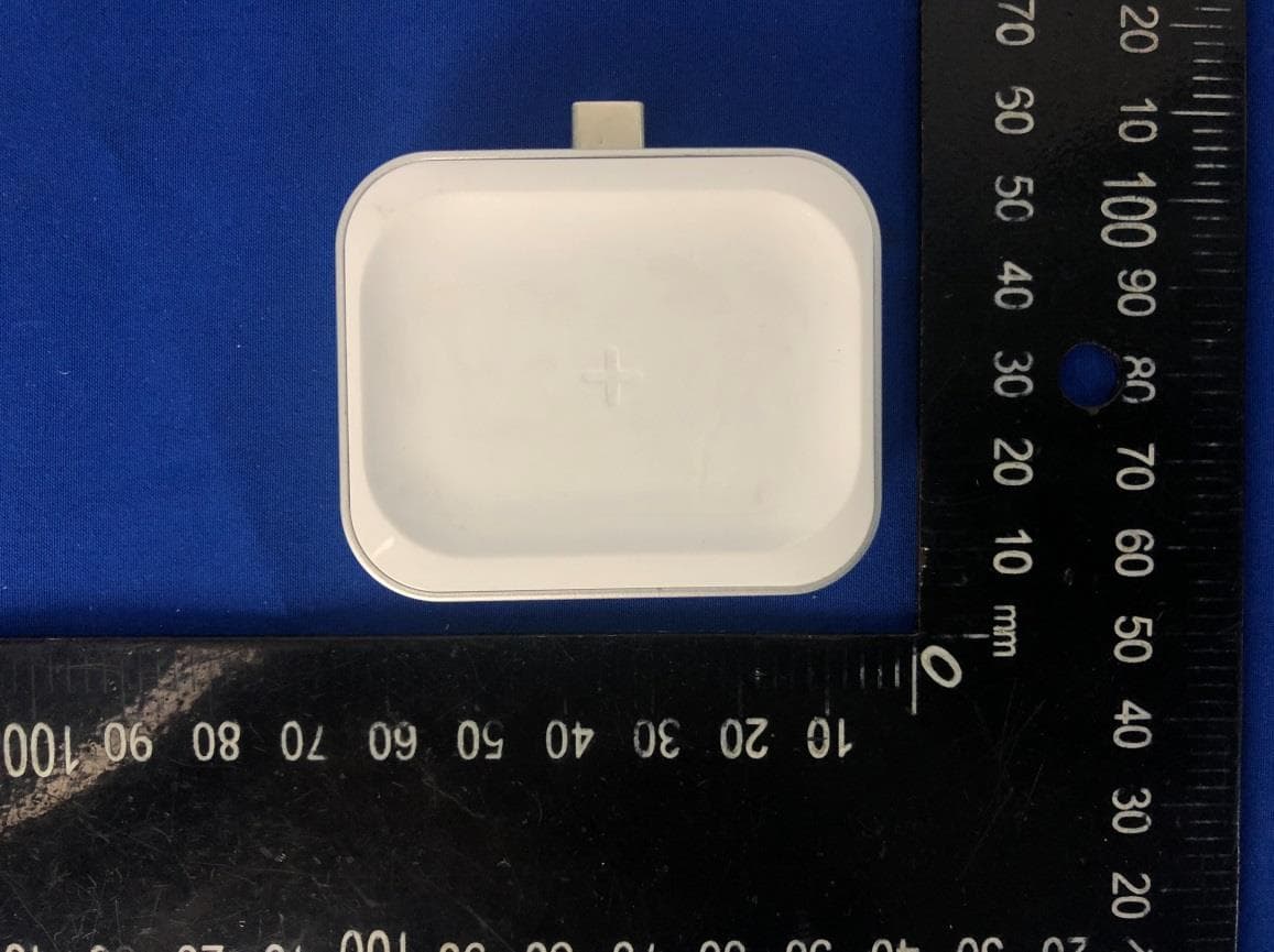
Click to zoom
Application Details
- Equipment Class
- DCD - Part 15 Low Power Transmitter Below 1705 kHz
- Date of Grant
- Jan 05, 2020
- Application Purpose
- Original Equipment
- Date of Application
- Jan 05, 2020
- Equipment Note
- wireless charging pad
- Frequency Range
- 0.11000000 - 0.20500000
- Company
- UBIO LABS, INC.
- Country
- United States
Documents & Files
Document Text
Text extracted from the exhibit documents filed with the FCC. Open a document above to read the original.
Users Manual
CMP item#: AWC1062 Description: Module, 10W Qi and Apple Watch Charger, USB-C In This document is proprietary & confidential. Do not copy or distribute without consent. Revision: 100 Date: 08/21/2019 Product Description The Ubio Labs AWC1062 is a compact, wireless charging module for AirPods and Apple Watch. It derives its power from a compatible USB-C receptacle capable of supplying power. Product Description Component - Product Requirements Document Industrial Design Component - Product Requirements Document CMP#: AWC1062SG Apple Dark Space Gray Apple White Accent USB-C Input Logo AirPods Surface Watch Surface Qi center Gasket Qi/Power LED Indicator Part Color / Material / Finish Notes Gasket Apple White / ABS / YS20019 AirPods Surface Apple White / ABS / Gloss Qi Center Apple White / ABS / Gloss Deboss 0.1mm Watch Surface Apple White / ABS / Gloss Accent Apple Dark Space Gray Light Blast / ABS / Paint Logo Clear/ Pad Print / Gloss Industrial Designer: Ken Jasinski STP File Name: AWC1062 Qi and Watch USB-C in_REV100.STEP Watch Module Industrial Design Component - Product Requirements Document CMP#: AWC1062SG - AL Apple Dark Space Gray Apple White Accent USB-C Input Logo AirPods Surface Watch Surface Qi center Gasket Qi/Power LED Indicator Part Color / Material / Finish Notes Gasket Apple White / ABS / YS20019 AirPods Surface Apple White / ABS / Gloss Qi Center Apple White / ABS / Gloss Deboss 0.1mm Watch Surface Apple White / ABS / Gloss Accent Apple Dark Space Gray / Aluminum / Light Blast Logo Clear/ Pad Print / Gloss Industrial Designer: Ken Jasinski STP File Name: AWC1062 Qi and Watch USB-C in_REV100.STEP Watch Module Industrial Design Component - Product Requirements Document CMP#: AWC1062NA Natural Aluminum Light Blast Apple White Accent USB-C Input Logo AirPods Surface Watch Surface Qi center Gasket Qi/Power LED Indicator Part Color / Material / Finish Notes Gasket Apple White / ABS / YS20019 AirPods Surface Apple White / ABS / Gloss Qi Center Apple White / ABS / Gloss Deboss 0.1mm Watch Surface Apple White / ABS / Gloss Accent Natural Aluminum Light Blast / ABS / Paint Logo Clear/ Pad Print / Gloss Industrial Designer: Ken Jasinski STP File Name: AWC1062 Qi and Watch USB-C in_REV100.STEP Watch Module Industrial Design Component - Product Requirements Document CMP#: AWC1062NA - AL Natural Aluminum Light Blast Apple White Accent USB-C Input Logo AirPods Surface Watch Surface Qi center Gasket Qi/Power LED Indicator Part Color / Material / Finish Notes Gasket Apple White / ABS / YS20019 AirPods Surface Apple White / ABS / Gloss Qi Center Apple White / ABS / Gloss Deboss 0.1mm Watch Surface Apple White / ABS / Gloss Accent Natural Aluminum / Aluminum / Light Blast Logo Clear/ Pad Print / Gloss Industrial Designer: Ken Jasinski STP File Name: AWC1062 Qi and Watch USB-C in_REV100.STEP Watch Module Industrial Design Component - Product Requirements Document CMP#: AWC1062 Silkscreen Logo Part Color / Material / Finish Notes Logo Clear/ Pad Print / Gloss Industrial Designer: Ken Jasinski .PDF File Name: AWC1062 Pad Print_Logo_REV100 Regulatory marking provided later – Please include in Quote Functional Requirements A.USB-C Input: The USB-C Input is used to provide power to the wireless charging module. Plugging the module into a compatible USB-C receptacle will automatically power up the module and remain on as long as the module is plugged in. B.Qi Coil: The Qi coil placed behind the top cover will allow charging of wireless AirPods case immediately upon placement on the coil location. This will initiate the Qi/Power Indicator functionality. C.Watch Charger: The Apple Magnetic charging module allows an Apple watch to magnetically attach and immediately begin charging. This will initiate the Qi/Power LED Indicator functionality. D.Qi/Power LED Indicator: The Qi/Power Indicator is a dual color White/Amber LED. It shall illuminate as described in the table above. E.Charge Priority: This product is designed to only charge one device at a time. If it does get subjected to two devices requesting a charge, the first device to initiate a charge handshake will take priority. The second device charging will be disabled during the first device charging duration. Component - Product Requirements Document Qi/Power LED Indicator Functionality Condition LED Status Notes Device Charging Illuminates white No device, not charging Not illuminated Fault Foreign Object Detection Illuminates amber for fault due to foreign object detection Input Power Illuminates white for 1 second at power up and then turns off if no device detected ON OFF D B C A Product Platform Overview Component - Product Requirements Document A.Platform Based Design: The AirPlugs product family shall be designed such that it is modular in nature for Hardware, Software, Mechanical functionality, design reusability and platformization. All adjustable variables such as time delays, duty cycles, frequencies etc. shall be software controlled to reduce impact to hardware in anticipation of standards and specification changes in the future. B.USB-C Current Platform: This platform accepts USB-C input from a compatible USB-C device. All end-user facing I/O’s, onboard I/O’s, interfaces and functionality pertaining to this platform shall be designed to comply with the applicable USB and MFi specifications. C.Indicator Platform: This platform provides the Indicator User Interface (UI) capability. All end-user facing I/O’s, onboard I/O’s, interfaces and functionality pertaining to this platform shall be designed to comply with the indicator functionality described here within this document. D.Wireless Charge Module Common Computing Platform (CCP): This platform provides the control logic and communication capabilities. All software functions, interfaces and libraries should be modular to align with hardware functionality and vice-versa. For example, USB-C Current I/O Platform Hardware and Software are modular and go together. Standard software devel…
Text truncated - open the document above for the full version.
Cover Letter(s)
1 Declaration Letter We, UBIO LABS, INC. declared that our product Wireless Charging Pad, item No.: AWC1062SG, AWC1062NA are identical inside, the electrical circuit design, layout, components used and internal wiring, with only difference being model name and color. Sincerely yours, Signature: Name/Title: Jason Lemenlson/ President Company Name: UBIO LABS, INC. Date:2019-12-25
Cover Letter(s)
UBIO LABS, INC. Agent Authorization Company: UBIO LABS, INC. Address: 2821 Northup Way, Suite 250, Bellevue, WA 98004, USA Product Name: wireless charging pad Model Number(s): AWC1062SG, AWC1062NA Product Description: wireless charging pad We authorize MiCOM Labs Inc., 575 Boulder Court, Pleasanton, California 94566, USA, to act on our behalf on all matters concerning the certification of above named equipment. We declare that MiCOM Labs Inc. is allowed to forward all information related to the approval and certification of equipment to the regulatory agencies as required and to discuss any issues concerning the approval application. Any and all acts carried out by MiCOM Labs on our behalf shall have the same effect as acts of our own. Signature: Date: 2019-12-27 Name: Jason Lemelson Title: President Company: UBIO LABS, INC.
Cover Letter(s)
UBIO LABS, INC. Office of Engineering Technology Federal Communications Commission 7435 Oakland Mills Road Columbia, MD 21046 USA Date: 2019-12-27 Subject; Request for Confidentiality FCC ID: 2ATGY-AWC1062 To Whom It May Concern, Pursuant to the provisions of the Commission’s rules Title 47 Sections §0.457 and §0.459, we are requesting the Commission to withhold the following attachment(s) as confidential documents from public disclosure indefinitely. These documents contain detailed system and equipment descriptions and are considered as proprietary information in operation of the equipment. The public disclosure of these documents might be harmful to our company and would give competitors an unfair advantage in the market. Schematic Diagram Block Diagram Parts List Operational Description Tune-up Procedure In additional to above mentioned documents, in order to comply with the marketing regulations in Title 47 CFR §2.803 and the importation rules in Title 47 CFR §2.1204, while ensuring that business sensitive information remains confidential until the actual marketing of newly authorized devices, we request Short Term Confidentiality of the following attachment(s); External Photos Test Setup Photos Internal Photos User Manual For 45 days, pursuant to Public Notice DA 04-1705. OR For 180 days pursuant to KDB 726920 D01. It is our understanding that all measurement test reports, FCC ID label format and correspondence during the certification review process cannot be granted as confidential documents and this information will be available for public review once the grant of equipment authorization is issued. Sincerely, Signature: Name: Jason Lemenlson Title: President
External Photos
Report No: CCISE191116801-1 Shenzhen Zhongjian Nanfang Testing Co., Ltd. Project No.: CCISE1911168 No. B-C, 1/F., Building 2, Laodong No.2 Industrial Park, Xixiang Road, Bao’an District, Shenzhen, Guangdong,China Telephone: +86 (0) 755 23118282 Fax: +86 (0) 755 23116366 Page 32 of 39 8 EUT Constructional Details Report No: CCISE191116801-1 Shenzhen Zhongjian Nanfang Testing Co., Ltd. Project No.: CCISE1911168 No. B-C, 1/F., Building 2, Laodong No.2 Industrial Park, Xixiang Road, Bao’an District, Shenzhen, Guangdong,China Telephone: +86 (0) 755 23118282 Fax: +86 (0) 755 23116366 Page 33 of 39 Report No: CCISE191116801-1 Shenzhen Zhongjian Nanfang Testing Co., Ltd. Project No.: CCISE1911168 No. B-C, 1/F., Building 2, Laodong No.2 Industrial Park, Xixiang Road, Bao’an District, Shenzhen, Guangdong,China Telephone: +86 (0) 755 23118282 Fax: +86 (0) 755 23116366 Page 34 of 39 Report No: CCISE191116801-1 Shenzhen Zhongjian Nanfang Testing Co., Ltd. Project No.: CCISE1911168 No. B-C, 1/F., Building 2, Laodong No.2 Industrial Park, Xixiang Road, Bao’an District, Shenzhen, Guangdong,China Telephone: +86 (0) 755 23118282 Fax: +86 (0) 755 23116366 Page 35 of 39
ID Label/Location Info
FCC ID: 2ATGY-AWC1062 IC: 25088-AWC1062
Internal Photos
Report No: CCISE191116801-1 Shenzhen Zhongjian Nanfang Testing Co., Ltd. Project No.: CCISE1911168 No. B-C, 1/F., Building 2, Laodong No.2 Industrial Park, Xixiang Road, Bao’an District, Shenzhen, Guangdong,China Telephone: +86 (0) 755 23118282 Fax: +86 (0) 755 23116366 Page 36 of 39 Report No: CCISE191116801-1 Shenzhen Zhongjian Nanfang Testing Co., Ltd. Project No.: CCISE1911168 No. B-C, 1/F., Building 2, Laodong No.2 Industrial Park, Xixiang Road, Bao’an District, Shenzhen, Guangdong,China Telephone: +86 (0) 755 23118282 Fax: +86 (0) 755 23116366 Page 37 of 39 Report No: CCISE191116801-1 Shenzhen Zhongjian Nanfang Testing Co., Ltd. Project No.: CCISE1911168 No. B-C, 1/F., Building 2, Laodong No.2 Industrial Park, Xixiang Road, Bao’an District, Shenzhen, Guangdong,China Telephone: +86 (0) 755 23118282 Fax: +86 (0) 755 23116366 Page 38 of 39 Report No: CCISE191116801-1 Shenzhen Zhongjian Nanfang Testing Co., Ltd. Project No.: CCISE1911168 No. B-C, 1/F., Building 2, Laodong No.2 Industrial Park, Xixiang Road, Bao’an District, Shenzhen, Guangdong,China Telephone: +86 (0) 755 23118282 Fax: +86 (0) 755 23116366 Page 39 of 39 ------End of report------
RF Exposure Info
Shenzhen ZhongjianNanfang Testing Co., Ltd. Report No: CCISE191116804V03 Authorized Signature: Bruce Zhang Laboratory Manager This report details the results of the testing carried out on one sample. The results contained in this test report do not relate to other samples of the same product and does not permit the use of theCCISproduct certification mark. The manufacturer should ensure that all products in series production are in conformity with the product sample detailed in this report. This report may only be reproduced and distributed in full. If the product in this report is used in any configuration other than that detailed in the report, the manufacturer must ensure the new system complies with all relevant standards. This document cannot be reproduced except in full, without prior written approval of the Company. Any unauthorized alteration, forgery orfalsification of the content or appearance of this document is unlawful and offenders may be prosecuted to the fullest extent of the law. Unless otherwise stated the results shown in this test report refer only to the sample(s) tested and such sample(s) are retained for 90 days only. 1 Cover Page RF Exposure Evaluation Report Applicant: UBIO LABS, INC. Address of Applicant: 2821 Northup Way, Suite 250, Bellevue, WA 98004, USA Equipment Under Test (EUT) Product Name: wireless charging pad Model No.: AWC1062SG, AWC1062NA Trade mark: ubiolabs FCC ID: 2ATGY-AWC1062 Applicable standards: FCC CFR Title 47 Part 2 Subpart J Section 2.1091 Date of sample receipt: 29Nov., 2019 Date of Test: 30Nov., to 02 Jan., 2020 Date of report issue: 06 Jan., 2020 Test Result: PASS* Report No: CCISE191116804V03 Shenzhen ZhongjianNanfang Testing Co., Ltd. Project No.:CCISE1911168 Bao’an District, Shenzhen, Guangdong,China Telephone: +86 (0) 755 23118282 Fax: +86 (0) 755 23116366 Page 2 of 9 2 Version Version No. Date Description 00 26 Dec., 2019 Original 01 02 Jan., 2020 Retest and Update page 6 02 03 Jan., 2020 Update page 7 03 06 Jan., 2020 Update page 8 Tested By: Date: 06 Jan., 2020 Test Engineer Reviewed By: Date: 06 Jan., 2020 Project Engineer Report No: CCISE191116804V03 Shenzhen ZhongjianNanfang Testing Co., Ltd. Project No.:CCISE1911168 Bao’an District, Shenzhen, Guangdong,China Telephone: +86 (0) 755 23118282 Fax: +86 (0) 755 23116366 Page 3 of 9 3 Contents Page 1 COVER PAGE ....................................................................................................................................................... 1 2 VERSION ............................................................................................................................................................... 2 3 CONTENTS ........................................................................................................................................................... 3 4 GENERAL INFORMATION .................................................................................................................................. 4 CLIENT INFORMATION .......................................................................................................................................................... 4 GENERAL DESCRIPTION OF E.U.T. ..................................................................................................................................... 4 OPERATING MODES ............................................................................................................................................................. 4 DESCRIPTION OF SUPPORT UNITS ...................................................................................................................................... 4 MEASUREMENT UNCERTAINTY ............................................................................................................................................ 4 ADDITIONS TO, DEVIATIONS, OR EXCLUSIONS FROM THE METHOD .................................................................................... 4 LABORATORY FACILITY ....................................................................................................................................................... 5 LABORATORY LOCATION..................................................................................................................................................... 5 TEST INSTRUMENTS LIST ..................................................................................................................................................... 5 5 TECHNICAL REQUIREMENTS SPECIFICATION IN FCC CFR TITLE 47 PART 2.1091 ............................ 6 LIMITS .................................................................................................................................................................................. 6 TEST SETUP BLOCK ............................................................................................................................................................ 6 LIMITS FORGENERAL POPULATION/UNCONTROLLED EXPOSURE ..................................................................................... 6 TEST PROCEDURE ............................................................................................................................................................... 7 RESULT ................................................................................................................................................................................ 8 6 TEST SETUP PHOTOS: .................................................................................................................................... 9 Report No: CCISE191116804V03 Shenzhen ZhongjianNanfang Testing Co., Ltd. Project No.:CCISE1911168 Bao’an District, Shenzhen, Guangdong,China Telephone: +86 (0) 755 23118282 Fax: +86 (0) 755 23116366 Page 4 of 9 4 General Information Client Information Applicant: UBIO LABS, INC. Address of Applicant: 2821 Northup Way, Suite 250, Bellevue, WA 98004, USA …
Text truncated - open the document above for the full version.
Test Report
Shenzhen Zhongjian Nanfang Testing Co., Ltd. Report No: CCISE191116801V01 Authorized Signature: Bruce Zhang Laboratory Manager This report details the results of the testing carried out on one sample. The results contained in this test report do not relate to other samples of the same product and does not permit the use of theCCISproduct certification mark. The manufacturer should ensure that all products in series production are in conformity with the product sample detailed in this report. This report may only be reproduced and distributed in full. If the product in this report is used in any configuration other than that detailed in the report, the manufacturer must ensure the new system complies with all relevant standards. This document cannot be reproduced except in full, without prior written approval of the Company. Any unauthorized alteration, forgery orfalsification of the content or appearance of this document is unlawful and offenders may be prosecuted to the fullest extent of the law. Unless otherwise stated the results shown in this test report refer only to the sample(s) tested and such sample(s) are retained for 90 days only. 1 Cover Page FCC REPORT Applicant: UBIO LABS, INC. Address of Applicant: 2821 Northup Way, Suite 250, Bellevue, WA 98004, USA Equipment Under Test (EUT) Product Name: wireless charging pad Model No.: AWC1062SG, AWC1062NA Trade mark: ubiolabs FCC ID: 2ATGY-AWC1062 Applicable standards: FCC CFR Title 47 Part 15 Subpart C Section 15.209 Date of sample receipt: 29 Nov., 2019 Date of Test: 30 Nov., to 25 Dec., 2019 Date of report issue: 02 Jan., 2020 Test Result: PASS * * In the configuration tested, the EUT complied with the standards specified above. Report No: CCISE191116801V01 Shenzhen Zhongjian Nanfang Testing Co., Ltd. Project No.: CCISE1911168 No. B-C, 1/F., Building 2, Laodong No.2 Industrial Park, Xixiang Road, Bao’an District, Shenzhen, Guangdong,China Telephone: +86 (0) 755 23118282 Fax: +86 (0) 755 23116366 Page 2 of 38 2 Version Version No. Date Description 00 26 Dec., 2019 Original 01 02 Jan., 2020 Update page 4 Prepared By: Date: 26 Dec., 2019 Report Clerk Check By: Date: 26 Dec., 2019 Project Engineer Report No: CCISE191116801V01 Shenzhen Zhongjian Nanfang Testing Co., Ltd. Project No.: CCISE1911168 No. B-C, 1/F., Building 2, Laodong No.2 Industrial Park, Xixiang Road, Bao’an District, Shenzhen, Guangdong,China Telephone: +86 (0) 755 23118282 Fax: +86 (0) 755 23116366 Page 3 of 38 3 Contents Page 1 COVER PAGE ....................................................................................................................................................... 1 2 VERSION ............................................................................................................................................................... 2 3 CONTENTS ........................................................................................................................................................... 3 4 TEST SUMMARY .................................................................................................................................................. 4 5 GENERAL INFORMATION .................................................................................................................................. 5 5.1 CLIENT INFORMATION ............................................................................................................................................ 5 5.2 GENERAL DESCRIPTION OF E.U.T. ....................................................................................................................... 5 5.3 TEST MODE ............................................................................................................................................................ 5 5.4 DESCRIPTION OF SUPPORT UNITS ........................................................................................................................ 5 5.5 MEASUREMENT UNCERTAINTY .............................................................................................................................. 5 5.6 DESCRIPTION OF CABLE USED ............................................................................................................................. 6 5.7 LABORATORY FACILITY .......................................................................................................................................... 6 5.8 LABORATORY LOCATION ....................................................................................................................................... 6 5.9 TEST INSTRUMENTSLIST ........................................................................................................................................ 7 6 TEST RESULTS ANDMEASUREMENT DATA ................................................................................................. 8 6.1 ANTENNA REQUIREMENT ....................................................................................................................................... 8 6.2 RADIATED EMISSION ............................................................................................................................................. 9 6.3 CONDUCTED EMISSION ....................................................................................................................................... 20 6.4 BANDWIDTH ......................................................................................................................................................... 25 7 TEST SETUP PHOTOS...................................................................................................................................... 28 8 EUT CONSTRUCTIONAL DETAILS ................................................................................................................ 31 Report No: CCISE191116801V01 Shenzhen Zhongjian Nanfang Testing Co., Ltd. Project No.: CCISE1911168 No. B-C, 1/F., Building 2, La…
Text truncated - open the document above for the full version.
Test Setup Photos
Report No: CCISE191116801 Shenzhen Zhongjian Nanfang Testing Co., Ltd. Project No.: CCISE1911168 No. B-C, 1/F., Building 2, Laodong No.2 Industrial Park, Xixiang Road, Bao’an District, Shenzhen, Guangdong,China Telephone: +86 (0) 755 23118282 Fax: +86 (0) 755 23116366 Page 28 of 38 7 Test Setup Photos Qi Inductive Output: Radiated Emission(9kHz-30MHz) Radiated Emission(30MHz-1000MHz) Report No: CCISE191116801 Shenzhen Zhongjian Nanfang Testing Co., Ltd. Project No.: CCISE1911168 No. B-C, 1/F., Building 2, Laodong No.2 Industrial Park, Xixiang Road, Bao’an District, Shenzhen, Guangdong,China Telephone: +86 (0) 755 23118282 Fax: +86 (0) 755 23116366 Page 29 of 38 Conducted Emission Magnetic Charge Output: Radiated Emission(9kHz-30MHz) Report No: CCISE191116801 Shenzhen Zhongjian Nanfang Testing Co., Ltd. Project No.: CCISE1911168 No. B-C, 1/F., Building 2, Laodong No.2 Industrial Park, Xixiang Road, Bao’an District, Shenzhen, Guangdong,China Telephone: +86 (0) 755 23118282 Fax: +86 (0) 755 23116366 Page 30 of 38 Radiated Emission(30MHz-1000MHz) Conducted Emission
Test Setup Photos
Report No: CCISE191116804V01 Shenzhen ZhongjianNanfang Testing Co., Ltd. Project No.:CCISE1911168 Bao’an District, Shenzhen, Guangdong,China Telephone: +86 (0) 755 23118282 Fax: +86 (0) 755 23116366 Page 9 of 9 6 Test Setup Photos: Qi Inductive Output Magnetic Charge Output ------End of report------
Contact Information
Applicant
Jesse Li(Compliance Manager)
Technical Contact
Test Firm
JianYan Testing Group Shenzhen Co., Ltd.Bruce Zhang
[email protected]+86 (0) 755 23118282
Technical Specifications
| # | Rule Parts | Frequency Range | Power Output |
|---|---|---|---|
| 1 | 15C | 0.11 MHz - 0.205 MHz | - |
Other Applications from UBIO LABS, INC.

2ATGY-AWC1109ABV
May 31, 2021Wireless Charging Stand
Equipment Class
DCD - Part 15 Low Power Transmitter Below 1705 kHz
2ATGY-AWC1098ABV
May 17, 2021Wireless Charging Pad
Equipment Class
DCD - Part 15 Low Power Transmitter Below 1705 kHz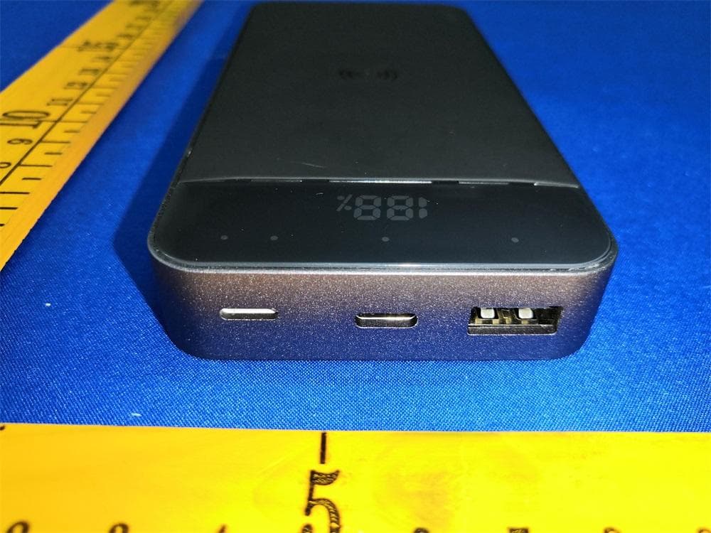
2ATGY-PWB1085SG
Apr 10, 2021Power Bank
Equipment Class
DXX - Part 15 Low Power Communication Device Transmitter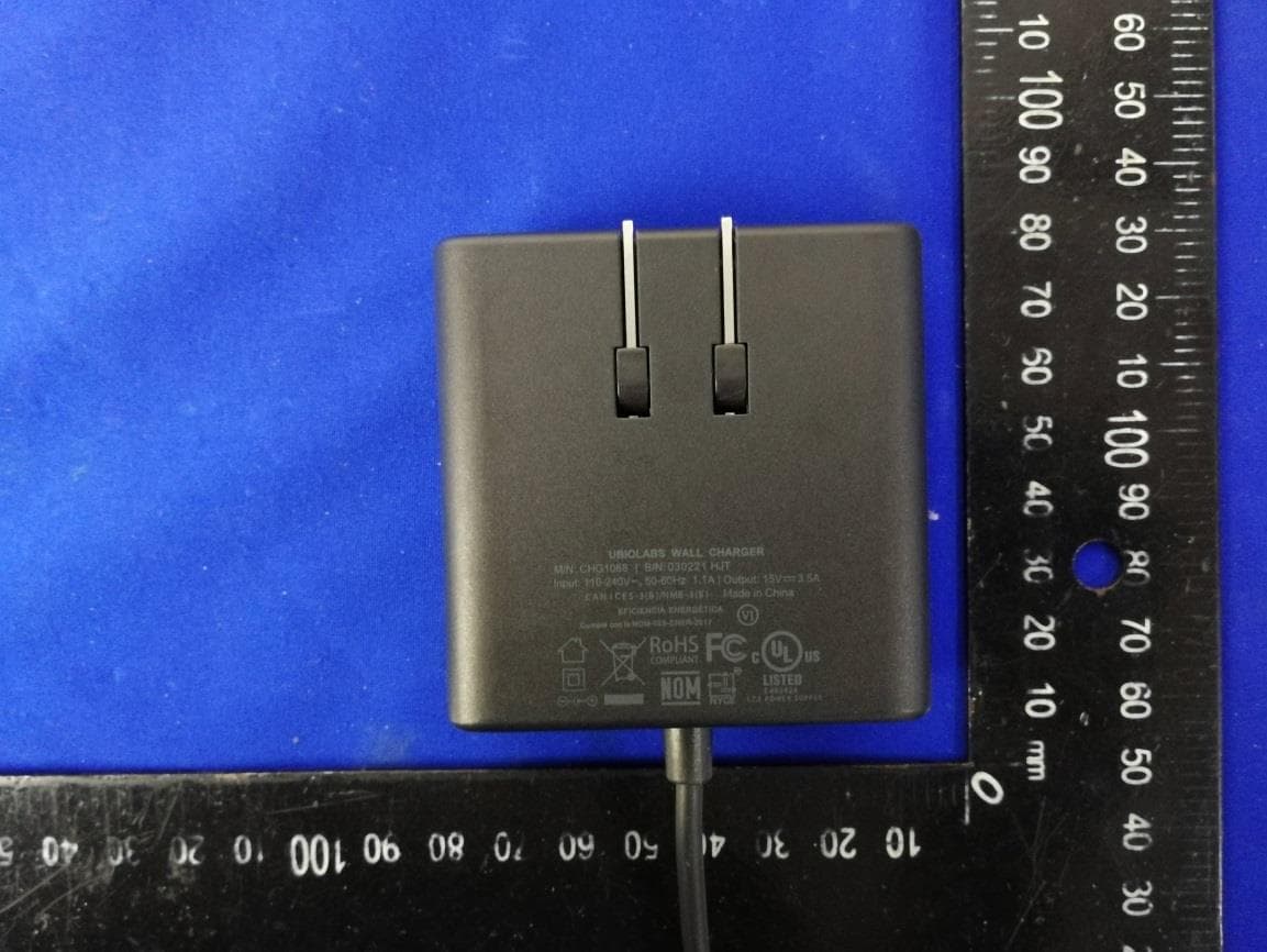
2ATGY-AWC1109
Mar 11, 2021Wireless Charging Stand
Equipment Class
DCD - Part 15 Low Power Transmitter Below 1705 kHz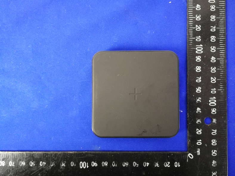
2ATGY-AWC1098
Feb 23, 2021Wireless Charging Pad
Equipment Class
DCD - Part 15 Low Power Transmitter Below 1705 kHz