2ATYV-BLE-MODULE-ABLE-MODULE-A
Scangrip A/S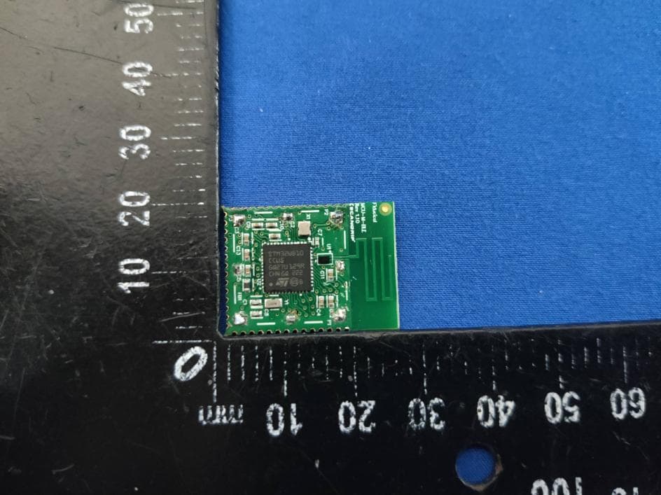
Click to zoom
Application Details
- Equipment Class
- DTS - Digital Transmission System
- Date of Grant
- Apr 13, 2023
- Application Purpose
- Original Equipment
- Date of Application
- Apr 13, 2023
- Equipment Note
- BLE-MODULE-A
- Frequency Range
- 2402.00000000 - 2480.00000000
- Company
- Scangrip A/S
- Country
- Denmark
Documents & Files
Document Text
Text extracted from the exhibit documents filed with the FCC. Open a document above to read the original.
Users Manual
This is information on a product in full production. June 2021DS13259 Rev 21/110 STM32WB10CC Multiprotocol wireless 32-bit MCU Arm ® -based Cortex ® -M4 with FPU, Bluetooth ® 5.2 radio solution Datasheet - production data Features •Includes ST state-of-the-art patented technology •Radio – 2.4 GHz –RF trans ceiver supporting Bluetooth ® 5.2 specification –RX sensitivity: -95.5 dBm (Bluetooth ® Low Energy at 1 Mbps and 2 Mbps) –Programmable output power up to +4 dBm with 1 dB steps –Integrated balun to reduce BOM –Support for 1 Mbps and 2 Mbps –Dedicated Arm ® 32-bit Cortex ® M0+ CPU for real-time Radio layer –Ac curate RSSI to enable power control –Suitable for sy stems requiring compliance with radio frequency regulations ETSI EN 300 328, EN 300 440, FCC CFR47 Part 15 and ARIB STD-T66 –Support for external PA –Available integrated passive device (IPD) companion chip for optimized matching solution (MLPF-WB-01E3) •Ultra-low-power platform – 2.0 to 3.6 V power supply – – 10 °C to +85 °C temperature range – 18 nA shutdown mode – 700 nA Standby mode + RTC + 48 KB RAM – Radio: Rx 7.7 mA / Tx at 0 dBm 8.6 mA Core: Arm ® 32-bit Cortex ® -M4 CPU with FPU, adaptive real-time accelerator (ART Accelerator) allowing 0-wait-state execution from Flash memory, frequency up to 64 MHz, MPU, 80 DMIPS and DSP instructions Performance benchmark – 1.25 DMIPS/MHz (Drystone 2.1) Supply and reset management – Ultra-safe, low-power BOR (brownout reset) with five selectable thresholds – Ultra-low-power POR/PDR – Programmable voltage detector (PVD) –V BAT mode with RTC and backup registers Clock sources – 32 MHz crystal oscillator with integrated trimming capacitors (Radio and CPU clock) – 32 kHz crystal oscillator for RTC (LSE) – Internal low-power 32 kHz RC (LSI1) – Internal low-drift 32 kHz (stability ±500 ppm) RC (LSI2) – Internal multispeed 100 kHz to 48 MHz oscillator, factory-trimmed – High speed internal 16 MHz factory trimmed RC (±1%) – 1x PLL for system clock and ADC Memories – 320 KB Flash memory with sector protection (PCROP) against R/W operations, enabling radio stack and application – 48 KB SRAM, including 36 KB with hardware parity check – 20x32-bit backup register – Boot loader supporting USART, SPI, I2C interfaces – 1 Kbyte (128 double words) OTP UFQFPN48 7 x 7 mm solder pad www.st.com STM32WB10CC 2/110DS13259 Rev 2 Rich analog peripherals (down to 2.0 V) – 12-bit ADC 2.5 Msps, 190 μA/Msps System peripherals – Inter processor communication controlle r (IPCC) for communication with Bluetooth ® Low Ene r gy – HW semaphores for resources sh aring between C PUs – 1x DMA controller (7x channels) supporting ADC, SPI, I2C, USART, AES, timers – 1x USART (ISO 7816, IrDA, SPI Master , Mod bus and Smartcard mode) – 1x SPI 32 Mbit/s – 1x I2C (SMBus/PMBus) – Touch sensing controller, up to eigh t se nsors – 1x 16-bit, four channels advanced timer – 1x 32-bit, four channels timer – 2x 16-bit ultra-low-power timer – 1x independent Systick – 1x independent watchdog – 1x window watchdog Security and ID – Secure firmware installation (SFI) fo r Blueto oth ® Low Energy SW stack – 2x hardware encryption AES maximum 25 6-bit for the application an d the Blueto oth ® Low Energy – HW public key authority (PKA) – Cryptographic algorithms : RSA, Dif fie-Helman, ECC over GF(p) – True random number generator (RNG) – Sector protection against R/W operat ion (PCROP) – CRC calculation unit – Die information: 96-bit unique ID – IEEE 64-bit unique ID. Possibility to derive Blueto oth ® Low Energy 48-bit EUI Up to 30 fast I/Os, 28 of them 5 V-tolerant Development support – Serial wire debug (SWD), JTAG fo r the a pplication processor – Application cross trigger Package is ECOPACK2 compliant DS13259 Rev 23/110 STM32WB10CCContents 5 Contents 1Introduction . . . . . . . . . . . . . . . . . . . . . . . . . . . . . . . . . . . . . . . . . . . . . . . . 9 2Description . . . . . . . . . . . . . . . . . . . . . . . . . . . . . . . . . . . . . . . . . . . . . . . . 10 3Functional overview . . . . . . . . . . . . . . . . . . . . . . . . . . . . . . . . . . . . . . . . 13 3.1Architecture . . . . . . . . . . . . . . . . . . . . . . . . . . . . . . . . . . . . . . . . . . . . . . . 13 3.2Arm ® Cortex ® -M4 core with FPU . . . . . . . . . . . . . . . . . . . . . . . . . . . . . . . 13 3.3Memories . . . . . . . . . . . . . . . . . . . . . . . . . . . . . . . . . . . . . . . . . . . . . . . . . 14 3.3.1Adaptive real-time memory accelerator (ART Accelerator) . . . . . . . . . . 14 3.3.2Memory protection unit . . . . . . . . . . . . . . . . . . . . . . . . . . . . . . . . . . . . . 14 3.3.3Embedded Flash memory . . . . . . . . . . . . . . . . . . . . . . . . . . . . . . . . . . . 14 3.3.4Embedded SRAM . . . . . . . . . . . . . . . . . . . . . . . . . . . . . . . . . . . . . . . . . 15 3.4Security and safety . . . . . . . . . . . . . . . . . . . . . . . . . . . . . . . . . . . . . . . . . . 16 3.5Boot modes and FW update . . . . . . . . . . . . . . . . . . . . . . . . . . . . . . . . . . . 16 3.6RF subsystem . . . . . . . . . . . . . . . . . . . . . . . . . . . . . . . . . . . . . . . . . . . . . 16 3.6.1RF front-end block diagram . . . . . . . . . . . . . . . . . . . . . . . . . . . . . . . . . . 17 3.6.2BLE general description . . . . . . . . . . . . . . . . . . . . . . . . . . . . . . . . . . . . . 18 3.6.3RF pin description . . . . . . . . . . . . . . . . . . . . . . . . . . . . . . . . . . . . . . . . . 19 3.6.4Typical RF application schematic . . . . . . . . . . . . . . . . . . . . . . . . . . . . . 19 3.7Power supply management . . . . . . . . . . . . . . . . . . . . . . . . . . . . . . . . . . . 20 3.7.1Power supply schemes . . . . . . . . . . . . . . . . . . . . . . . . . . . . . . . . . . . . . 20 3.7.2Linear voltage regulator . . . . . . . . . . . . . . . . . . . . . . . . . . . . . . . . . . . . . 23 3.7.3Power supply supervisor . . . . . . . . . . . . . . . . . . . . . . . . . . . . . . . . . . . . 23 3.7.4Low-power modes …
Text truncated - open the document above for the full version.
Cover Letter(s)
CSF410-TCB 8.0 Page 1 of 5 FORM CSF410-TCB FCC APPLICATION FORM This form constitutes the certification agreement between Element Materials Technology and the Applicant and is required for every application. Please ensure accuracy when completing this form because the content is used to make the FCC upload to the FCC eFiling system. Please complete the relevant sections in the tables below. Guidance on each numbered section of this form is provided at the end of the document. Please contact Element if you have any further questions. Applicant business details 1. Applicant’s complete, legal business name. Scangrip A/S 2. Applicant’s mailing address (Line 1) Rytterhaven 9, DK-5700 Svendborg, Denmark 3. Applicant’s mailing address (Line 2) 4. City, State, Zip (or postal code) DK-5700 Svendborg 5. Name, Title of Person registered with the FCC to receive the grant. Jasar Elezaj, Quality Manager 6. Phone No. (Area/Country/City Code, Number, Ext). +45 6320 6320 7. Fax No. (Area/Country/City Code, Number, Ext. +45 6320 6321 8. Internet email address [email protected] 9. Applicants FRN # (FCC registered number) 0028640357 Authorised agent details Only to be completed where a third party is used to make an application on behalf of the Applicant 10. Name, Title 11. Mailing address (Line 1) 12. City, State, Zip (or postal code) 13. Phone No. (Area/Country/City Code, Number, Ext). 14. Internet email address Product details 15. Equipment model 310.084 16. FCC ID Number GRANTEE CODE 2ATYV 17. FCC ID equipment code (Max. 14 Chars.) -BLE-MODULE-A 18. FCC ID Rule part. (15.249, 15.247, etc.) 15.247 FORM CSF410-TCB FCC APPLICATION FORM CSF410-TCB 8.0 Page 2 of 5 19.Type of grant ■Original Grant ☐ Class II Permissive Change ☐Class III Permissive Change ☐Change in ID (Provide original FCC ID number and grant date (yyyy/mm/dd: ) 20.Seeking modular approval? ■Yes☐No 21.Contain a pre-approved radio module? ☐Yes ■No If yes, FCC ID of pre-approved module: 22.Is the device a software defined radio (SDR)? Other information 23.Do you wish to hold some information permanently confidential? ■Yes☐No 24.Do you wish to hold some information confidential short-term? ☐Yes■No Notes or comments BLE: 2402-2480MHz Free field ☐Yes■No FORM CSF410-TCB FCC APPLICATION FORM CSF410-TCB 8.0 Page 3 of 5 FCC application and signature Read each certification carefully before answering and signing this application. WILLFUL FALSE STATEMENTS MADE ON THIS FORM ARE PUNISHABLE BY FINE AND/OR IMPRISONMENT (U.S. CODE, TITLE 18, SECTION 1001), AND/OR REVOCATION OF ANY STATION LICENSE OR CONSTRUCTION PERMIT (U.S. CODE, TITLE 47, SECTION 312(a)(1)), AND/OR FORFEITURE (U.S. CODE, TITLE 47, SECTION 503). 25.SECTION 5301 (ANTI-DRUG ABUSE) CERTIFICATION The applicant must certify that neither the applicant nor any party to the application is subject to a denial of Federal benefits, that include FCC benefits, pursuant to Section 5301 of the Anti-Drug Abuse Act of 1988, 21 U.S.C. §862 because of a conviction for possession or distribution of a controlled substance. See 47 CFR 1.2002(b) for the definition of a “party” for these purposes. Does the applicant or authorized agent so certify? ■Yes☐No 26.NOT PREVIOUSLY SUBMITTED NOR DENIED I certify that this product has not been previously submitted to the FCC nor to another TCB for certification. I further certify that this product has not previously been dismissed nor denied by the FCC nor by another TCB. 27.APPLICANT/AGENT ATTESTATION I certify that I am authorized to sign this application. All of the statements herein and the exhibits attached hereto are true and correct to the best of my knowledge and belief. In accepting a Grant of Equipment Authorization issued by the TCB as a result of the representations made in this application, the applicant is responsible for (1) labeling the equipment with the exact FCC ID specified in this application, (2) compliance statement labeling pursuant to the applicable rules, and (3) compliance of the equipment with the applicable technical rules. If the applicant is not the actual manufacturer of the equipment, appropriate arrangements have been made with the manufacturer to ensure that production units of this equipment will continue to comply with the FCC’s technical requirements. Authorizing an agent to sign this application, is done solely at the applicant’s discretion; however, the applicant remains responsible for all statements in this application. If an agent has signed this application on behalf of the applicant, a written letter of authorization which includes information to enable the agent to respond to the above Section 5301 (Anti-Drug Abuse) Certification statement has been provided by the applicant. It is understood that the letter of authorization must be submitted to the FCC upon request, and that the TCB reserves the right to contact the applicant directly at any time. 28.IEC/ISO 17065 and IAF/ILAC REQUIREMENTS By signing this application, the applicant agrees to the following requirements and conditions: a.The applicant will always comply with the relevant provisions of the certification programme, and the requirements of the regulatory body under which certification is granted, including implementing appropriate changes when they are communicated by the Element Certification Body. b.If the certification applies to ongoing production, the certified product continues to fulfil the product requirements. c.The applicant will make all necessary arrangements for: i)the conduct of the evaluation, including provision for examining documentation and records and access to and access to the relevant equipment, location(s), area(s), personnel, and applicant's subcontractors; ii)investigation of complaints; iii)the participation of observers, if applicable. d.The applicant makes claims regarding certification consistent with the scope of certification. e.The applicant will not use its product certification in such a manner as to bring the Element Certification Bo…
Text truncated - open the document above for the full version.
Cover Letter(s)
Scangrip A/S LETTER OF AGENCY Date: April 6. 2023 Element Materials Technology 100 Frobisher Business Park Malvern Worcestershire WR14 1BX UK FCC ID: 2ATYV-BLE-MODULE-A To Whom It May Concern: We certify that we are not subject to denial of federal benefits, that includes FCC benefits, pursuant to Section 5301 of the Anti-Drug Abuse ACT of 1988, U.S.C. 862. Further, no party, as defined in 47 CFR 1.2002(b), to the application, is subject to denial of federal benefits, that includes FCC benefits. Thank you for your attention to this matter. Yours faithfully company Sincerely, Printed Name: Jasar Elezaj Company: Scangrip A/S Job Title: Quality Manager Email: [email protected] Telephone: +45 6320 6320
Cover Letter(s)
MODULAR APPROVAL LETTER [Scangrip A/S] [April 6, 2023] Dear Application Examiner: [Scangrip A/S, 310.084, 2ATYV-BLE-MODULE-A] is seeking single modular approval. The radio meets the requirements for modular approval as detailed in FCC 15.212. Compliance to each of the requirements is described below: 1. “The modular transmitter must have its own RF shielding.” The radio portion of the module is contained in its own RF shielding. The shielding is installed at the factory. Please see the Internal Photos exhibit. 2. “The modular transmitter must have buffered modulation/data inputs.” The EUT has buffered data inputs to insure compliance with Part 15 requirements under conditions of excessive data rates or over-modulation. Please see the Schematics exhibit. 3. “The modular transmitter must have its own power supply regulation.” The EUT has its own power supply regulation to insure compliance with Part 15 requirements regardless of the quality or level of external DC supplying the module from the host unit. Please see Schematics exhibit. Also, the technical report exhibit contains AC power line conducted emissions data taken with the EUT powered from a linear power supply that contains no EMC suppression components. 4. “The modular transmitter must comply with the antenna requirements of Section 15.203 and 15.204(c).” The EUT meets the FCC antenna requirements. Please see Antenna information exhibit and internal photos exhibit. 5. “The modular transmitter must be tested in a stand-alone configuration.” The EUT was tested in a stand-alone configuration. The module was greater than 10 cm from the host device. Please see test setup photos exhibit and technical report exhibit. 6. “The modular transmitter must be labeled with its own FCC ID number.” The EUT is labeled with its own FCC ID number. Please see FCC ID label & location exhibit. If the FCC ID number will not be visible when the module is installed inside a host device, another label with the FCC ID will be applied to the exterior of the host device. 7. “The modular transmitter must comply with any specific rule or operating requirements applicable to the transmitter and the manufacturer must provide adequate instructions along with the module to explain any such requirements.” The EUT is compliant with all applicable FCC rules. Detail instructions for maintaining compliance are given in the User Manual. 8. “The modular transmitter must comply with any applicable RF exposure requirements.” The EUT is compliant with all applicable RF exposure requirements. Please see RF Exposure Exhibit. Please contact me if you have additional questions. Your attention to this matter is greatly appreciated. Best regards, Printed Name: Jasar Elezaj Company: Scangrip A/S Job Title: Quality Manager Email: [email protected] Telephone: +45 6320 6320
Cover Letter(s)
SCANGRIP A/S Request for Confidentiality Letter-FCC Date:April 6, 2023 Federal Communications Commission Authorization and Evaluation Division 7435 Oakland Mills Road Columbia, Maryland 21046 Re: Request for confidentiality FCC ID: 2ATYV-BLE-MODULE-A To whom it may concern, We hereby respectfully request that under the provision of 47 CFR 0.459 and 0.457(d) the documents listed below and attached with this application for certification be provided with confidential status. Schematics.pdf Operational Description.pdf Frequency Block Diagrams.pdf Any exhibit / information for which we have requested confidentiality, but which may not be accorded such treatment by the FCC, should be returned to us. The documents listed above contain trade secrets that are treated as confidential by us. Substantial competitive harm to us could result should they be made available to the public. Sincerely, Printed Name: Jasar Elezaj Company: Scangrip A/S Job Title: Quality Manager Email: [email protected] Telephone: +45 6320 6320
External Photos
FCC ID: 2ATYV-BLE-MODULE-A FCC ID: 2ATYV-BLE-MODULE-A
ID Label/Location Info
FCC ID: 2ATYV-BLE-MODULE-A
Internal Photos
FCC ID: 2ATYV-BLE-MODULE-A FCC ID: 2ATYV-BLE-MODULE-A
Operational Description
Introduction This application note is dedicated to the STM32WB Series microcontrollers. One of the main reasons to use a PCB (printed circuit board) antenna is the reduced overall cost of the radio module. Well designed and implemented PCB-printed antennas have a similar performance to the SMD (surface-mounted device) ceramic equivalence. In general, the footprint for a ceramic SMD antenna is smaller than that for a PCB-printed variant. For a PCB-printed antenna solution, the increased size of the PCB in relation to space required for the antenna means that the radio module is larger and the cost of the PCB increased. However the PCB solution is generally cheaper than a SMD ceramic antenna. The demonstration and development boards for the STM32WB Series implement PCB printed antenna based on this application note. Low cost PCB antenna for 2.4 GHz radio: meander design for STM32WB Series AN5129 Application note AN5129 - Rev 4 - April 2019 For further information contact your local STMicroelectronics sales office. www.st.com 1General information This document applies to STM32WB Series Arm ® -based devices. Note:Arm is a registered trademark of Arm Limited (or its subsidiaries) in the US and/or elsewhere. AN5129 General information AN5129 - Rev 4 page 2/22 2Coordinate system For the purpose of this document, the spherical coordinate system illustrated in the figure below is used. Figure 1. Spherical coordinate system The PCB module is orientated vertically (plane X-Z) and located in proximity to the origin of the coordinate system. The azimuth angle radiates from the X-axis towards the Y-axis and the elevation angle radiates from the Z-axis towards the horizontal X-Y plane. Sometimes, as with geographical and navigational systems, the X-axis is called the "Nord-axis", the Yaxis is called the "East-axis" and the Z-axis is called the "Zenith-axis". AN5129 Coordinate system AN5129 - Rev 4 page 3/22 3Layout specification The PCB antennas, including the electrical parameters of PCB materials used, are layout sensitive. It is recommended to use a layout as close as possible to the one shown in the figure below. Figure 2. PCB antenna dimensions (in mm) The electrical parameters and performance of the PCB antenna are also determined by the substrate used, in particular the thickness of the core and dielectric constants. AN5129 Layout specification AN5129 - Rev 4 page 4/22 The figure below illustrates a typical cross-section of the substrate in a PCB-antennae area. Figure 3. PCB cross section at antennae area A substrate with the parameters as defined in the table below is recommended. Table 1. Recommended substrate specification Layer Dimensions Dielectric constant Ɛ R LabelValue (mil)Value (μm) Solder mask, topS10.717.784.4 Copper traceT1.640.64- CoreC28711.24.4 Solder mask, bottomS20.717.784.4 AN5129 Layout specification AN5129 - Rev 4 page 5/22 4Impedance matching Meander-like PCB antenna can be tuned to the required 50 Ω impedance by matching the impedance circuitry with the π topology. In Figure 2, the impedance matching area is marked with a dashed line. Under nominal conditions, this antenna exhibits and impedance very close to the required nominal impedance (50 Ω). To check the performance of this design, a sample antenna was manufactured (according to the specifications covered by this document). The figure below shows this antenna. Figure 4. Part of 802.15.4 and BLE PCB with meander-like antenna (scale around 4:1) Assuming that the manufactured sample exhibits the expected performance (no impedance matching necessary), the impedance matching circuitry is bypassed by two 100 pF capacitors connected in series, as shown in the figure below. Figure 5. Bypassing impedance matching circuitry - Direct RF connection All electrical parameters of the meander-like antenna have been measured at connection to the band-pass filter (BPF) with the frequency span covering frequencies from 2.4 GHz to 2.5 GHz. AN5129 Impedance matching AN5129 - Rev 4 page 6/22 Complex impedance of the antenna is shown in the Smith diagram in the figure below. Figure 6. Complex impedance of the meander-like antenna (Smith chart) The figure below shows the magnitude of the S11 parameter (in log scale). Figure 7. S11 parameter in logarithmic scale (Cartesian plot) AN5129 Impedance matching AN5129 - Rev 4 page 7/22 The figure below shows the standing wave ratio (SWR). Figure 8. Antenna standing wave ratio (SWR) The following changes affect the radiation impedance of the PCB antenna: • slight board size variation • metal shielding • use of plastic cover • presence of other components in proximity of the antenna The best performance impedance matching circuitry compensates these effects so that, for operating frequencies, the optimum 50 Ω impedance is achieved. AN5129 Impedance matching AN5129 - Rev 4 page 8/22 5Radiation pattern, 3-D visualization A three-dimensional (3-D) visualization of the radiation pattern (magnitude of the electrical far field |E|) is done for the center ISM band frequency 2.44175 GHz. Figure 9. 3-D radiation pattern overview Figure 10. Radiation pattern on X-Z plane AN5129 Radiation pattern, 3-D visualization AN5129 - Rev 4 page 9/22 6Radiation pattern, 2-D visualization In this section, all radiation patterns are related to the magnitude of electrical far field |E|, that is normalized and shown in the logarithmic scale (in dB). This means that the maximum global radiation pattern (maximum magnitude of the electrical far-field E) is represented by 0 dB level. To show the antenna radiation patterns in detail, three two dimensional (2-D) major cuts are presented. Consider the orientation of the module in the spherical coordinate system as shown in Figure 1. A three dimensional (3-D) far field radiation pattern is visualized as three two dimensional (2-D) cuts through a 3- D pattern. The following major planes are used for these cuts (see Figure 11): • one horizontal X-Y plane • two vertical planes: X-Z plan…
Text truncated - open the document above for the full version.
RF Exposure Info
FCC ID: 2ATYV-BLE-MODULE-A Prediction of MPE at a given distance 1. Limits The criteria listed in the following table shall be used to evaluate the environment impact of human exposure to radio frequency (RF) radiation as specified in 1.1307(b) 2. Test Procedure Equation from page 18 of OET Bulletin 65, Edition 97-01 Where: S = power density P = power input to the antenna G = numeric gain of the antenna in the direction of interest relative to an isotropic radiator R = distance to the centre of radiation of the antenna FCC ID: 2ATYV-BLE-MODULE-A 3. Result Worse case is as below: Mode Frequency (MHz) Prediction distance (cm) RF output power MPE (mW/cm 2 ) Limit (mW/cm 2 ) SAR Test Exclusion dBm mW BLE 2M 2402 20 3.96 2.489 0.0012 1 Yes Then SAR evaluation is not required.
Test Report
ALPHA's reports is using a digital certificate that is trusted on Adobe's official server. If there is no digital certificate or the digital certificate shows damaged in your report. Please do not accept the report. E-mail: [email protected] Tel: 4008-3008-95Website:http://www.a-lab.cn RF REPORT On Behalf of FCC ID: 2ATYV-BLE-MODULE-A Scangrip A/S FCC ID: 2ATYV-BLE-MODULE-A BLE-MODULE-A Model No.: 310.084 Prepared for : Scangrip A/S Address : Rytterhaven 9, DK-5700 Svendborg, Denmark Prepared By : Shenzhen Alpha Product Testing Co., Ltd Address : Building i, No.2, Lixin Road, Fuyong Street, Bao'an District, 518103, Shenzhen, Guangdong, China Report Number : A2303118-C01-R01 Date of Receipt : November 17, 2022 Date of Test : November 17, 2022 to March 28, 2023 Date of Report : March 28, 2023 Version Number : V0 Page2 of52 Report No.: A2303118-C01-R01 TABLE OF CONTENTS Description Page 1 General Information .............................................................................................................................. 5 1.1 Description of Device (EUT) ....................................................................................................... 5 1.2 Test Lab information ................................................................................................................... 5 2 Summary of test .................................................................................................................................... 6 2.1 Test Standard description: ......................................................................................................... 6 2.2 Summary of test .......................................................................................................................... 6 2.3 Test Mode Description ................................................................................................................ 7 2.4 Test Equipment ............................................................................................................................ 8 3 Evaluation Results (Evaluation) ......................................................................................................... 10 3.1 Antenna requirement ................................................................................................................ 10 3.1.1 Conclusion: ...................................................................................................................... 10 4 Radio Spectrum Matter Test Results (RF) .......................................................................................... 11 4.1 Conducted Emission at AC power line .................................................................................... 11 4.1.1 E.U.T. Operation: .............................................................................................................. 11 4.1.2 Test Setup Diagram: ......................................................................................................... 11 4.1.3 Test Result: ...................................................................................................................... 12 4.2 Occupied Bandwidth ................................................................................................................ 14 4.2.1 E.U.T. Operation: ............................................................................................................. 14 4.2.2 Test Setup Diagram: ........................................................................................................ 14 4.2.3 Test Result: ...................................................................................................................... 15 4.3 Maximum Conducted Output Power ....................................................................................... 23 4.3.1 E.U.T. Operation: ............................................................................................................. 23 4.3.2 Test Setup Diagram: ........................................................................................................ 23 4.3.3 Test Result: ...................................................................................................................... 24 4.4 Power Spectral Density ............................................................................................................ 27 4.4.1 E.U.T. Operation: ............................................................................................................. 27 4.4.2 Test Setup Diagram: ........................................................................................................ 27 4.4.3 Test Result: ...................................................................................................................... 28 4.5 Emissions in non-restricted frequency bands ....................................................................... 31 4.5.1 E.U.T. Operation: ............................................................................................................. 31 4.5.2 Test Setup Diagram: ........................................................................................................ 31 4.5.3 Test Result: ...................................................................................................................... 32 4.6 Band edge emissions ............................................................................................................... 36 4.6.1 E.U.T. Operation: ............................................................................................................. 36 4.6.2 Test Result: ...................................................................................................................... 37 4.7 Emissions in restricted frequency bands (below 1GHz) ....................................................... 43 4.7.1 E.U.T. Operation: ............................................................................................................. 43 4.…
Text truncated - open the document above for the full version.
Test Setup Photos
FCC ID: 2ATYV-BLE-MODULE-A Conducted Emission at AC power line FCC ID: 2ATYV-BLE-MODULE-A Band edge emissions Emissions in restricted frequency bands (above 1GHz) FCC ID: 2ATYV-BLE-MODULE-A Emissions in restricted frequency bands (below 1GHz)
Contact Information
Applicant
Jasar Elezaj(Quality Manager)
Test Firm
Shenzhen Alpha Product Testing Co., LTD.Real Yak
[email protected]+86 755 29766001
Technical Specifications
| # | Rule Parts | Frequency Range | Power Output |
|---|---|---|---|
| 1 | 15C | 2.40 GHz - 2.48 GHz | 2.50 mW |