2AUKD-SY-O511BTACREO OpenBuds Kids
Dongguan Shangyuan Electronics Co., Ltd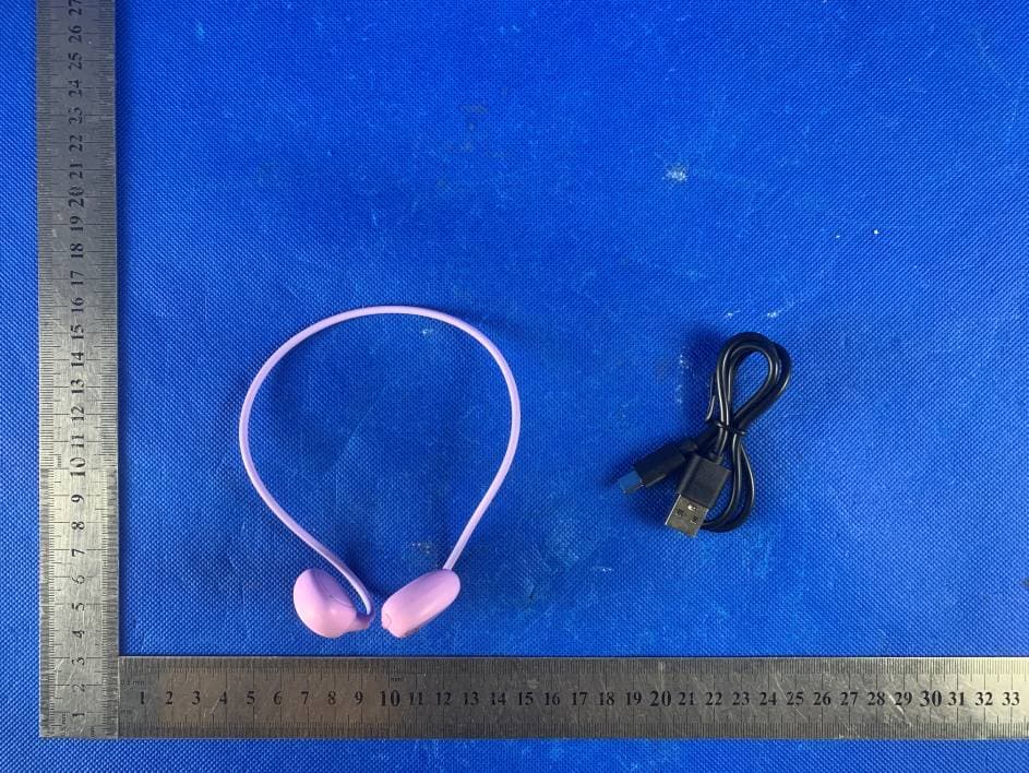
Click to zoom
Application Details
- Equipment Class
- DSS - Part 15 Spread Spectrum Transmitter
- Date of Grant
- Mar 27, 2023
- Application Purpose
- Original Equipment
- Date of Application
- Mar 27, 2023
- Equipment Note
- ACREO OpenBuds Kids
- Frequency Range
- 2402.00000000 - 2480.00000000
- Country
- Hong Kong
Documents & Files
Document Text
Text extracted from the exhibit documents filed with the FCC. Open a document above to read the original.
Users Manual
80X100mm Touch Control Instructions If the headset is stuck or other functions cannot be used normally, you can click " " red and blue lights on twice for 3 seconds, the red and blue lights will flash alternately, and the headset will be restored to factory Settings. 1 x USB Type-C Cable Model: OpenBuds Kids 1 X ACREO OpenBuds Kids 1 × User Manual Package Contents LED Indicator Function Instructions How to Charge the Headphone 1. When using the OpenBuds Kids for the first time, please power on the headphones via touch and hold for 5 seconds, the headphone will automatically come into the pairing mode. 2. If the product is in pairing mode, it will display"ACREO OpenBuds Kids" as the Bluetooth name on the smartphone, please select and connect. The Next Generation Open Ear Headphones for Kids The Next Generation Open Ear Headphones for Kids Model: OpenBuds Kids Touch area Type-C Charging Port HeadBand with Memory Steel Wire Type-c charging port Charging instructions: When charging indicator light, red light is steady on. When fully charged, turn on the blue light. Quick Start Guide Restore factory settings Press and hold " " for 5 seconds Press and hold " " for 5 seconds Press " " 3 times Press " " 2 times Press " " 1 times Press " " 4 times Press " " 5 times Short press " " 1 time when calling Short press " " for 2 times continuously Press " " for 2 seconds during incoming call Power on Power Off Volume + Volume - Previous Track Next Track Play/Pause Answer/Hang up Restore factory settings Reject to Answer the Call LED indicator Instructions Pairing Mode--Red and blue light flash alternately Connected Mode--Blue light flashes 1 time at 5 seconds interval Make sure the headphone is fully charged before first use. 1. The headphone has a built-in li-on battery, which must be charged at least once every 2 months if it is not used for a long time. 2. Use the USB type C cable to charge the headphone, you can use any USB power input 5V 500mA adapter included, and the computer USB port is fine. 3. When charging, the headphone will automatically shut down, and the indicator light shows below ACREO OpenBuds Kids Touch and hold for 5 seconds 3. After being connected successfully, it will be ready to play music, make calls, and so on. Note When the headphone is not in the connection status for more than 5 minutes, the headphone will automatically shut down. This equipment has been tested and found to comply with the limits for a Class B digital device, pursuant to part 15 of the FCC Rules. These limits are designed to provide reasonable protection against harmful interference in a residential installation. This equipment generates, uses and can radiate radio frequency energy and, if not installed and used in accordance with the instructions, may cause harmful interference to radio communications. However, there is no guarantee that interference will not occur in a particular installation. If this equipment does cause harmful interference to radio or television reception, which can be determined by turning the equipment off and on, the user is encouraged to try to correct the interference by one or more of the following measures: •Reorient or relocate the receiving antenna. •Increase the separation between the equipment and receiver. •Connect the equipment into an outlet on a circuit different from that to which the receiver is connected. •Consult the dealer or an experienced radio/TV technician for help. Caution: Any changes or modifications to this device not explicitly approved by manufacturer could void your authority to operate this equipment. This device complies with part 15 of the FCC Rules. Operation is subject to the following two conditions: (1) This device may not cause harmful interference, and (2) this device must accept any interference received, including interference that may cause undesired operation. RF Exposure Information The device has been evaluated to meet general RF exposure requirement. The device can be used in portable exposure condition without restriction. FCC Statement
Attestation Statements
- D on gguan Shangyuan Electronics Co.,Ltd - Federal Communications Commission Authorization and Evaluation Division Equipment Authorization Branch 7435 Oakland Mills Road Columbia, MD 21046 3/16/23 U.S. Aqent Desiqnation Dongguan Shangyuan Electronics Co.,Ltd acknowledges their consent for the following contact located in the United States to act as their agent for service of process for the equipment for which authorization is sought (FCC ID: 2AUKD-SY-0511 BT): Name and company of U.S. agent: Stone Trading Limited Physical U.S. address of agent: 6547 N Academy Blvd #2266,Colorado Springs.CO 80918,United States FRN of U.S. agent: 0033401936 Email address of U.S. agent: Email:compliance@c-shlink .com Stone Trading Limited acknowledges thei『obligationto accept service of process on behalf of Dongguan Shangyuan Electronics Co.,Ltd. Dongguan Shangyuan Electronics Co.,Ltd accepts its obligation to maintain an agent for service of process in the United States for no less than one year after either the grantee has permanently terminated all marketing and importation of the applicable equipment within the U.S., or the conclusion of any Commission-related administrative or judicial proceeding involving the equipment, whichever is later. By signing this form, we confirm the above and that we are aware of the application requirements listed under§2.911 (d)(7). Sincerely , EO>“n , (L)(p)(16 ' Z:-1U� 吵,,-sn (ppo E u] 1oc寸 Signature [Name)Mia Long [T i U e ] M a n a g e r [Company] Dongguan Shangyuan Electronics Co.,Ltd 翌 ` [Name of U.S. a gent] Dongmei Fang [Title of U.S. agent] Manager [Company of U.S. agent] Stone Trading Limited 写 The i n formation provided in this letter is based on the referenced rule parts of Title 47 of the CFR as well as KDB 986446 DOI. An expiration date for this letter does not exist. In case the U.S. age n t cha n ges, the grantee is obligated to notify the FCC. 扫描全能王
External Photos
Page 1 of 5 FCC ID: 2AUKD-SY-O511BT Dongguan Yaxu (AiT) Technology Limited No.22, Jinqianling 3rd Street, Jitigang, Huangjiang, Dongguan, Guangdong, China. External Photos Photo 1 Photo 2 Page 2 of 5 FCC ID: 2AUKD-SY-O511BT Dongguan Yaxu (AiT) Technology Limited No.22, Jinqianling 3rd Street, Jitigang, Huangjiang, Dongguan, Guangdong, China. Photo 3 Photo 4 Page 3 of 5 FCC ID: 2AUKD-SY-O511BT Dongguan Yaxu (AiT) Technology Limited No.22, Jinqianling 3rd Street, Jitigang, Huangjiang, Dongguan, Guangdong, China. Photo 5 Photo 6 Page 4 of 5 FCC ID: 2AUKD-SY-O511BT Dongguan Yaxu (AiT) Technology Limited No.22, Jinqianling 3rd Street, Jitigang, Huangjiang, Dongguan, Guangdong, China. Photo 7 Photo 8 Page 5 of 5 FCC ID: 2AUKD-SY-O511BT Dongguan Yaxu (AiT) Technology Limited No.22, Jinqianling 3rd Street, Jitigang, Huangjiang, Dongguan, Guangdong, China. Photo 9 ------End------
ID Label/Location Info
Label FCC ID: 2AUKD-SY-O511BT
Internal Photos
Page 1 of 3 FCC ID: 2AUKD-SY-O511BT Dongguan Yaxu (AiT) Technology Limited No.22, Jinqianling 3rd Street, Jitigang, Huangjiang, Dongguan, Guangdong, China. Internal Photos Photo 1 Photo 2 Antenna Page 2 of 3 FCC ID: 2AUKD-SY-O511BT Dongguan Yaxu (AiT) Technology Limited No.22, Jinqianling 3rd Street, Jitigang, Huangjiang, Dongguan, Guangdong, China. Photo 3 Photo 4 Page 3 of 3 FCC ID: 2AUKD-SY-O511BT Dongguan Yaxu (AiT) Technology Limited No.22, Jinqianling 3rd Street, Jitigang, Huangjiang, Dongguan, Guangdong, China. Photo 5 ------End------
RF Exposure Info
Page 1 of 2 Report No.: AIT23010905FH1 RF EXPOSURE EVALUATION 1. PRODUCT INFORMATION Product Description ACREO OpenBuds Kids Model Name SY-O511BT FCC ID 2AUKD-SY-O511BT 2. Applicable Standard According to §1.1307(b)(1), systems operating under the provisions of this section shall be operated in a manner that ensures that the public is not exposed to radio frequency energy level in excess of the Commission’s guidelines. According to §1.1310 and §2.1093 RF exposure requirement KDB447498 v06: Mobile and Portable Devices RF Exposure Procedures and Equipment Authorization Policies 3. Requirement According to KDB447498 D01 General RF Exposure Guidance v06 Section 4.3.1 Standalone SAR test exclusion considerations: “Unless specifically required by the published RF exposure KDB procedures, standalone 1-g head or body and 10-g extremity SAR evaluation for general population exposure conditions, by measurement or numerical simulation, is not required when the corresponding SAR Test Exclusion Threshold condition, listed below, is satisfied. These test exclusion conditions are based on source-based time-averaged maximum conducted output power of the RF channel requiring evaluation, adjusted for tune-up tolerance, and the minimum test separation distance required for the exposure conditions.22 The minimum test separation distance is determined by the smallest distance from the antenna and radiating structures or outer surface of the device, according to the host form factor, exposure conditions and platform requirements, to any part of the body or extremity of a user or bystander (see 5) of section 4.1). To qualify for SAR test exclusion, the test separation distances applied must be fully explained and justified by the operating configurations and exposure conditions of the transmitter and applicable host platform requirements, typically in the SAR measurement or SAR analysis report, according to the required published RF exposure KDB procedures. When no other RF exposure testing or reporting is required, a statement of justification and compliance must be included in the equipment approval, in lieu of the SAR report, to qualify for the SAR test exclusion. When required, the device specific conditions described in the other published RF exposure KDB procedures must be satisfied before applying these SAR test exclusion provisions; for example, handheld PTT two-way radios, handsets, laptops & tablets etc.23 “ [(max. power of channel, including tune-up tolerance, mW)/ (min. test separation distance, mm)] · [√f (GHz)] ≤ 3.0 for 1-g SAR and ≤ 7.5 for 10-g extremity SAR, where: • f (GHz) is the RF channel transmit frequency in GHz • Power and distance are rounded to the nearest mW and mm before calculation Page 2 of 2 Report No.: AIT23010905FH1 • The result is rounded to one decimal place for comparison • 3.0 and 7.5 are referred to as the numeric thresholds in the step 2 below The test exclusions are applicable only when the minimum test separation distance is ≤ 50 mm and for transmission frequencies between 100 MHz and 6 GHz. When the minimum test separation distance is < 5 mm, a distance of 5 mm according to 5) in section 4.1 is applied to determine SAR test exclusion. 4. Manufacturing Tolerance Mode Max. Peak Conducted Output Power (dBm) Max. tune-up Antenna Antenna BT 2.19 3±1 5. Standalone MPE Result Antenna 1 Band/Mode f (GHz) Antenna Distance (mm) RF output power including tune up SAR Test Exclusion Threshold SAR Test Exclusion Estimated SAR dBm mW BT 2.5 5 4 2.51 0.794< 3 Yes 0.1059 Note: Only the worst case recorded. 6. Conclusion : Compliance the RF exposure requirement
Test Report
Page 1 of 38 Report No.: AIT23010905W1 Dongguan Yaxu (AiT) Technology Limited No.22, Jinqianling 3rd Street, Jitigang, Huangjiang, Dongguan, Guangdong, China. TEST REPORT Client Information: Applicant: Dongguan Shangyuan Electronics Co., Ltd Applicant add.: Room D9, 6/F, Block 2 Camel Paint Building, 62 Hoi Yuen Road, Kwun Tong, Kowloon, Hong Kong Manufacturer: Dongguan Shangyuan Electronics Co., Ltd Manufacturer add.: Room D9, 6/F, Block 2 Camel Paint Building, 62 Hoi Yuen Road, Kwun Tong, Kowloon, Hong Kong Product Information: Product Name: ACREO OpenBuds Kids Model No.: SY-O511BT Brand Name: N/A FCC ID: 2AUKD-SY-O511BT Applicable standards: FCC CFR Title 47 Part 15 Subpart C Section 15.247 Prepared By: Dongguan Yaxu (AiT) Technology Limited No.22, Jinqianling 3rd Street, Jitigang, Huangjiang,Dongguan, Guangdong, China Tel.: +86-769-8202 0499 Fax.: +86-769-8202 0495 Date of Receipt: Jan. 09, 2023 Date of Test: Jan. 09, 2022~ Jan. 11, 2023 Date of Issue: Jan. 12, 2023 Test Result: Pass This device described above has been tested by Dongguan Yaxu (AiT) Technology Limited and the test results show that the equipment under test (EUT) is in compliance with the FCC requirements. And it is applicable only to the tested sample identified in the report. Note: This report shall not be reproduced except in full, without the written approval of Dongguan Yaxu (AiT) Technology Limited, this document may be altered or revised by Dongguan Yaxu (AiT) Technology Limited, personal only, and shall be noted in the revision of the document. This test report must not be used by the client to claim product endorsement. Reviewed by: Approved by: Simba Huang Seal.chen Page 2 of 38 Report No.: AIT23010905W1 Dongguan Yaxu (AiT) Technology Limited No.22, Jinqianling 3rd Street, Jitigang, Huangjiang, Dongguan, Guangdong, China. 1 Contents Page COVER PAGE 1 CONTENTS .................................................................................................................................................................... 2 2 TEST SUMMARY .......................................................................................................................................................... 4 2.1 Statement of the Measurement Uncertainty .............................................................................. 4 2.2 Measurement Uncertainty ......................................................................................................... 4 3 TEST FACILITY ............................................................................................................................................................. 5 3.1 Deviation from standard ............................................................................................................ 5 3.2 Abnormalities from standard conditions .................................................................................... 5 3.3 Test Location ............................................................................................................................. 5 4 GENERAL INFORMATION ......................................................................................................................................... 6 4.1 Test frequencies ........................................................................................................................ 7 4.2 EUT Peripheral List ................................................................................................................... 8 4.3 Test Peripheral List ................................................................................................................... 8 4.4 TEST METHODOLOGY............................................................................................................ 9 4.5 Description of Test Modes ....................................................................................................... 10 5 EQUIPMENT USED DURING TEST ........................................................................................................................ 11 6 TEST RESULTS AND MEASUREMENT DATA .................................................................................................... 12 6.1 Antenna requirement .............................................................................................................. 12 6.2 Peak Power Measurement ...................................................................................................... 13 6.3 Frequency Separation and 20 dB Bandwidth .......................................................................... 15 6.4 Number of Hopping Frequency ............................................................................................... 17 6.5 Time of Occupancy (Dwell Time) ............................................................................................ 18 6.6 Conducted Spurious Emissions and Band Edges Test ........................................................... 20 6.7 Restrict-band Band-edge Measurements ............................................................................... 22 6.8 Radiated Emissions Measurement ......................................................................................... 24 6.9 Conducted Emissions ............................................................................................................. 34 6.10 Pseudorandom frequency hopping sequence ......................................................................... 37 7 TEST SETUP PHOTOGRAPHS OF EUT ................................................................................................................ 38 8 EXTERNAL PHOTOGRAPHS OF EUT ................................................................................................................... 38 9 INTERNAL PHOTOGRAPHS OF EUT .................................................................................................................... 38 Page 3 of 38 Report No.: AIT23010905W1 Dongguan Yaxu (A…
Text truncated - open the document above for the full version.
Test Report
SPECIFICATION FOR APPROVAL 客戶名稱 CUSTOMER : 客戶料號 CUSTOMER’S P/N : 料號 PART NUMBER : WAN3216F245C0X 規格 DESCRIPTION : Chip Antenna 3216 L Ant 2.45G Type 02,04,06 版本 VERSION : V3.1 日期 ISSUE DATE : 客 戶 承 認 CUSTOMER APPROVED 工 程 部 R&D CENTER 承 認 APPROVAL 確 認 CHECKED 製 作 DRAWN Ray James Thor 2/11 Chip antenna For Bluetooth / WLAN Applications Dimension (mm) L 3.23 ± 0.20 W 1.66 ± 0.20 T 0.45 ± 0.20 P/N: WAN3216F245C02 WAN3216F245C04 WAN3216F245C06 3/11 Part Number Information WAN 3216 F 245 C 0X A B C D E F A Product Series Antenna B Dimension L x W 3.2X1.6mm (+-0.2mm) C Material High K material D Working Frequency 2.4 ~ 2.5GHz E Feeding mode PIFA & Single Feeding F Antenna type 0X=02,04,06 / Type=02,04,06 1. Electrical Specification Remark : Bandwidth & Peak Gain was measured under evaluation board of next page Specification Part Number WAN3216F245C02 WAN3216F245C04 WAN3216F245C06 Central Frequency 2450 MHz Bandwidth 120 (Min.) MHz Return Loss -6.5 (Max) dB Peak Gain 0 dBi Impedance 50 Ohm Operating Temperature -40~+85 °C Maximum Power 4 W Resistance to Soldering Heats 10 ( @ 260°C) sec. Polarization Linear Azimuth Beamwidth Omni-directional Termination Ni / Au (Leadless) 4/11 2. Recommended PCB Pattern Evaluation Board Dimension 2 nd Evaluation Board Dimension Suggested Matching Circuit 5/11 FootPrint (Unit : mm) Matching Circuit 50 ohm transmission Line 6/11 3. Measurement Results Return Loss 7/11 Radiation Pattern Efficiency Peak Gain Directivity 2450MHz 76.65% 0.00 dBi 2.69 dBi Chamber Coordinate System X Y Z 8/11 4.Reliability and Test Condictions ITEM REQUIREMENTS TEST CONDITION Solderability 1. Wetting shall exceed 90% coverage 2. No visible mechanical damage Pre-heating temperature:150°C/60sec. Solder temperature:230±5°C Duration:4±1sec. Solder:Sn-Ag3.0-Cu0.5 Flux for lead free: rosin Solder heat Resistance 1. No visible mechanical damage 2. Central Freq. change :within ± 6% 10±0.5 sec. 60sec .. TEMP (°C) 150°C 260°C Pre-heating temperature:150°C/60sec. Solder temperature:260±5°C Duration:10±0.5sec. Solder:Sn-Ag3.0-Cu0.5 Flux for lead free: rosin Component Adhesion (Push test) 1. No visible mechanical damage The device should be reflow soldered(230±5°C for 10sec.) to a tinned copper substrate A dynometer force gauge should be applied the side of the component. The device must with-ST-F 0.5 Kg without failure of the termination attached to component. Component Adhesion (Pull test) 1. No visible mechanical damage Insert 10cm wire into the remaining open eye bend ,the ends of even wire lengths upward and wind together. Terminal shall not be remarkably damaged. Thermal shock 1. No visible mechanical damage 2. Central Freq. change :within ±6% Phase Temperature(°C) Time(min) 1 +85±5°C 30±3 2 Room Temperature Within 3sec 3 -40±2°C 30±3 4 Room Temperature Within 3sec +85°C=>30±3min -40°C=>30±3min Test cycle:10 cycles The chip shall be stabilized at normal condition for 2~3 hours before measuring. Resistance to High Temperature 1. No visible mechanical damage 2. Central Freq. change :within ±6% 3. No disconnection or short circuit. Temperature: 85±5°C Duration: 1000±12hrs The chip shall be stabilized at normal condition for 2~3 hours before measuring. Resistance to Low Temperature 1. No visible mechanical damage 2. Central Freq. change :within ±6% 3. No disconnection or short circuit. Temperature:-40±5°C Duration: 1000±12hrs The chip shall be stabilized at normal condition for 2~3 hours before measuring. Humidity 1. No visible mechanical damage 2. Central Freq. change :within ±6% 3. No disconnection or short circuit. Temperature: 40±2°C Humidity: 90% to 95% RH Duration: 1000±12hrs The chip shall be stabilized at normal condition for 2~3 hours before measuring. 4±1 sec. 60sec TEMP (°C) 150°C 230°C 9/11 5.Soldering and Mounting Mildly activated rosin fluxes are preferred. The minimum amount of solder can lead to damage from the stresses caused by the difference in coefficients of expansion between solder, chip and substrate. The terminations are suitable for all wave and re-flow soldering systems. If hand soldering cannot be avoided, the preferred technique is the utilization of hot air soldering tools. Recommended temperature profiles for re-flow soldering in Figure 1. Products attachment with a soldering iron is discouraged due to the inherent process control limitations. In the event that a soldering iron must be employed the following precautions are recommended. ‧Preheat circuit and products to 150°C ‧Never contact the ceramic with the iron tip ‧Use a 20 watt soldering iron with tip diameter of 1.0mm ‧280°C tip temperature (max) ‧1.0mm tip diameter (max) ‧Limit soldering time to 3 sec. SOLDERING COOLING NATURAL PRE-HEATING TEMPERATURE(°C) 60~120 s 10s max. 30~60s 250~260 230 180 150 TIME(sec.) Reflow Soldering SOLDERING COOLING NATURAL PRE-HEATING TEMPERATURE(°C) within 3s Gradualcooling 150 TIME(sec.) Iron Soldering Over 60s 350 300 10/11 6.Packaging Information Tape Specification: Reel Specification: (7’’, Φ180 mm) Tape Width(mm) A(mm) B(mm) C(mm) D(mm) Chip/Reel(pcs) 8 9.0±0.5 60±2 13.5±0.5 178±2 3000 11/11 7.Storage and Transportation Information Storage Conditions To maintain the solderability of terminal electrodes: 1. Temperature and humidity conditions: -10~ 40°C and 30~70% RH. 2. Recommended products should be used within 6 months from the time of delivery. 3. The packaging material should be kept where no chlorine or sulfur exists in the air. Transportation Conditions 1. Products should be handled with care to avoid damage or contamination from perspiration and skin oils. 2. The use of tweezers or vacuum pick up is strongly recommended for individual components. 3. Bulk handling should ensure that abrasion and mechanical shock are minimized.
Test Report
Dongguan Yaxu(AiT) Technology Limited Report No.: AIT23010905W1 FCC ID: 2AUKD-SY-O511BT Page 1 of 42 Appendix A RF Test Data for BT(BDR/EDR) (Conducted Measurement) Product Name: ACREO OpenBuds Kids Trade Mark: N/A Test Model: SY-O511BT Environmental Conditions Temperature: 23.5°C Relative Humidity: 52.8% ATM Pressure: 101Kpa Test Engineer: Simba Huang Supervised by: Seal Chen Dongguan Yaxu(AiT) Technology Limited Report No.: AIT23010905W1 FCC ID: 2AUKD-SY-O511BT Page 2 of 42 Contents Page COVER PAGE 1 Duty Cycle ........................................................................................................................................................................................... 3 1.1 Test Result ............................................................................................................................................................................... 3 1.2 Test Graphs ............................................................................................................................................................................. 4 2 Maximum Conducted Peak Output Power .......................................................................................................................................... 7 2.1 Test Result ............................................................................................................................................................................... 7 2.2 Test Graphs ............................................................................................................................................................................. 8 3 20dB Bandwidth ................................................................................................................................................................................ 11 3.1 Test Result ............................................................................................................................................................................. 11 3.2 Test Graphs ........................................................................................................................................................................... 12 4 Carrier Frequency Separation ........................................................................................................................................................... 15 4.1 Test Result ............................................................................................................................................................................. 15 4.2 Test Graphs ........................................................................................................................................................................... 16 5 Hopping Channel Number ................................................................................................................................................................. 17 5.1 Test Result ............................................................................................................................................................................. 17 5.2 Test Graphs ........................................................................................................................................................................... 18 6 Dwell Time ......................................................................................................................................................................................... 19 6.1 Test Result ............................................................................................................................................................................. 19 6.2 Test Graphs ........................................................................................................................................................................... 20 7 RF Conducted Spurious Emissions ................................................................................................................................................... 22 7.1 Test Result ............................................................................................................................................................................. 22 7.2 Test Graphs ........................................................................................................................................................................... 23 8 Band-edge for RF Conducted Emissions .......................................................................................................................................... 29 8.1 Test Result ............................................................................................................................................................................. 29 8.2 Test Graphs ........................................................................................................................................................................... 30 9 Restrict-band band-edge measurements .......................................................................................................................................... 38 9.1 Test Result ............................................................................................................................................................................. 38 9.2 Test Graphs ........................................................................................................................................................................... 39 Dongguan Yaxu(AiT) Technology Limited Report No.: AIT23010905W1 FCC ID: 2AUKD-SY-O511BT Page 3 of 42 1 Duty Cycle 1.1 Test Result Mode Frequency (MHz) Duty Cycle (%) 1/T (kHz) 1-DH1 2402 31.46 2.56 1-DH1 2441 31.2 2.63 1-DH1 2480 31.92 2.56 2-DH1 2402 32 2.56 2-DH1 2441 32 2.56 2-DH1 2480 32 2.56 Dongguan Yaxu(AiT) Technolog…
Text truncated - open the document above for the full version.
Test Setup Photos
Page 1 of 2 FCC ID: 2AUKD-SY-O511BT Dongguan Yaxu (AiT) Technology Limited No.22, Jinqianling 3rd Street, Jitigang, Huangjiang, Dongguan, Guangdong, China. Test Setup Photo Radiated Emission Page 2 of 2 FCC ID: 2AUKD-SY-O511BT Dongguan Yaxu (AiT) Technology Limited No.22, Jinqianling 3rd Street, Jitigang, Huangjiang, Dongguan, Guangdong, China. Conducted Emission ------End------
Contact Information
Applicant
Mia Long(Manager)
Test Firm
Dongguan Yaxu (AiT) Technology LimitedCoin Tang
[email protected]+86 0769-82020499-21
Technical Specifications
| # | Rule Parts | Frequency Range | Power Output |
|---|---|---|---|
| 1 | 15C | 2.40 GHz - 2.48 GHz | 1.70 mW |
Other Applications from Dongguan Shangyuan Electronics Co., Ltd
2AUKD-U8
Nov 24, 2025Headphones
Equipment Class
DSS - Part 15 Spread Spectrum Transmitter2AUKD-JH20
Sep 28, 2025Wireless Headphones
Equipment Class
DSS - Part 15 Spread Spectrum Transmitter2AUKD-JCH-01
Jul 27, 2022Wireless Headphones
Equipment Class
DSS - Part 15 Spread Spectrum Transmitter
2AUKD-BTH12
Jul 30, 2020Wireless headphones
Equipment Class
DSS - Part 15 Spread Spectrum Transmitter