Text extracted from the exhibit documents filed with the FCC. Open a document above to read the original.
User Manual Product Name: EM3587 ZigBee Module Model Name: DSM-001 1. Product introduction 1.1 Summary DSM-001 ZigBee wireless module, based on silicon labs EM358x series chip, has high performance, low power consumption, works in ISM band, fully supports IEEE802.15.4 standard, supports ZigBee-PRO protocol Stack. 1.2 Performance characteristics Complete System-on-Chip -32-bit ARM® Cortex -M3 processor -2.4 GHz IEEE 802.15.4-2003 transceiver & lower MAC -256 or 512 kB flash, with optional read protection -32 or 64 kB RAM memory -AES128 encryption accelerator Low power consumption, advanced management -RX Current (w/ CPU): 27 mA -TX Current (w/ CPU, +3 dBm TX): 31 mA -Low deep sleep current, with retained RAM and GPIO: 1.0 uA without/1.25 uA with sleep timer -Low-frequency internal RC oscillator for low-power sleep timing -High-frequency internal RC oscillator for fast (110 μs) processor start-up from sleep Exceptional RF Performance -Normal mode link budget up to 103 dB; configurable up to 110 dB -–100 dBm normal RX sensitivity; configurable to –102 dBm (1% PER, 20 byte packet) 1.3 Application scenario Internet of Things Industrial control Smart Home Intelligent lighting Smart Remote control Health Environmental monitoring 2 Hardware Description 2.1 Pin Description The pins of the DSM-001 series module are shown below. NoName of PinTypeDirectionDescription 1 GND GNDPowerGND 2 GND GNDPowerGND 33.3VVCCPower Supply Voltage 3.3V 43.3VVCCPower Supply Voltage 3.3V 5 NC // / 6 PC7 CMOSI/O General IO port 7 PWM2 CMOSI/O PWM2 8NC/// 9PWM1 PWM1 10 PB0 CMOSI/O General IO port 11 I2C_SDA CMOSI/O Two Wire serial Interface- data port 12 I2C_SCL CMOSI/O Two Wire serial Interface- clock port 13 PA0 CMOSI/O General IO port 14 PA3 CMOSI/O General IO port 15 NC / // 16 NC / // 17 NC / // 18 NC / // 19 NC / // 20 NC // / 21 PB5 CMOSI/O General IO port 22 PB6 CMOSI/O General IO port 23 PB7 CMOS I/OGeneral IO port 24 NC / // 25 PC1 CMOS I/OGeneral IO port 26 PB3 CMOS I/OGeneral IO port 27 NC // / 28 NC // / 29 NC // / 30 NC // / 31 RX CMOSI/O UART RX 32 TX CMOSI/O UART tx 33 PA6 CMOS I/OGeneral IO port 34 NC // / 35 NC // / 36 NC // / 37 NC // / 38 NC // / 39 NC // / 40 NC // / 2.2 Package size The following figure shows the dimensions of the DSM-001 module. Including shield height 3.4 ±0.2mm. 3. Specifications 3.1 Electrical characteristics limit parameters Modules must be within the conditions described below and may cause damage beyond the range described in the table below. ParameterMin.Max. Supply voltage-0.3V3.6V All pins-0.3V VDD+0.3V Stored temperature -40ºC150ºC 3.2 Working conditions ParameterMin.Max. Working voltage2.0V3.6V Environmental temperature -40ºC85ºC 3.3 Working current Test conditions VDD=3.0V @ +25°C Operating modeMin.Max. Sleep mode1uA1.25uA RF reception 27mA28mA RF transmission 31mA60mA 3.4 RF characteristics Receiving sensitivity-102dBm Transmit power15.52dBm Center frequency offset±40ppmincluding temperature range and aging RF output impedance 50Ω 4 Welding Reflow soldering is recommended to operate according to the temperature curve shown below. Temperature 25~160°C 160~ 190°C >220°C220°C~Pk. Pk. Temp (235°C) Target time(s) 90~13030~60 20-5010-15150-270 5. Certification FCC OEM Guidance 1. Applicable FCC rules This module is granted by Single Modular Approval. It complies to the requirements of FCC part 15C, section 15.247 rules. 2. The specific operational use conditions This module can be used in IoT devices. The input voltage to the module is nominally 3.3V DC. The operational ambient temperature of the module is -40 to 85 degree C. Only the embedded PCB antenna is allowed. Any other external antenna is prohibited. 3. Limited module procedures Not Limited module 4. Trace antenna design Not using Trace antenna design 5. RF exposure considerations The equipment complies with FCC radiation exposure limits set forth for an uncontrolled environment. This equipment should be installed and operated with minimum distance 20cm between the radiator and your body. If the equipment built into a host as a portable usage, the additional RF exposure evaluation may be required as specified by 2.1093. 6. Antenna Antenna type: PCB antenna; Peak gain: 0 dBi 7. Label and compliance information An exterior label on OEM’s end product can use wording such as the following: “Contains Transmitter Module FCC ID: 2AV5NMSWUP-310” or “Contains FCC ID: 2AV5NMSWUP-310.” 8. Information on test modes and additional testing requirements a)The modular transmitter has been fully tested by the module grantee on the required number of channels,modulation types, and modes, it should not be necessary for the host installer to re-test all the available transmitter modes or settings. It is recommended that the host product manufacturer, installing the modular transmitter,perform some investigative measurements to confirm that the resulting composite system does not exceed the spurious emissions limits or band edge limits (e.g., where a different antenna may be causing additional emissions). b)The testing should check for emissions that may occur due to the intermixing of emissions with the other transmitters, digital circuitry, or due to physical properties of the host product (enclosure). This investigation is especially important when integrating multiple modular transmitters where the certification is based on testing each of them in a stand-alone configuration. It is important to note that host product manufacturers should not assume that because the modular transmitter is certified that they do not have any responsibility for final product compliance. c) If the investigation indicates a compliance concern the host product manufacturer is obligated to mitigate the issue. Host products using a modular transmitter are subject to all the applicable individual technical rules as well as to the general conditions of operation in Sections 15.5, 15.15, and 15.29 to not cause interference. The operator of the host product wil…
Text truncated - open the document above for the full version.
Company: Hefei DappWo rks Technology Co. Ltd. Add: Room 611-166, R&D Center Building International Intelligent Voice Industrial Park, 3333 Xiyou Road, High-tech Zone, Hefei, China Tel: 18757285495 Fax: N/A E-mail: [email protected] FCC Confidential Authorization Date: 2020-03-27 FEDERAL COMMUNICATIONS COMMISSIONS Authorization and Evaluation Division 7435 Oakland Mills Road Columbia, MD 21046 Subject: Confidentiality Request regarding application for certification of FCC ID: 2AV5NMSWUP-310 To: whom it may concern, In accordance with Sections 0.457 and 0.459 of the Commission’s Rules, Hefei DappWorks Technology Co. Ltd. hereby requests long-term confiden tial treatment of information accompanying this application as outlined below: Block Diagram Schematics Operation Description The above m aterials contain proprietary and confidential information not customarily released to the public. The public disclosure of these materials provides unjustified benefits to its competitors in the market. Sincerely Yours, Signature: Printed Name: Xiaojun Deng Title: Manager
Applicant Hefei DappWorks Technology Co. Ltd. FCC ID: 2AV5NMSWUP-310 Section 15.212 Modular Transmitters Request for Modular Approval Request for Limited Modular Approval RequirementsEUT ConditionsComply(Y/N) Single Modular Approval Requirements 1 The radio elements of the modular transmitter must have their own shielding. The physical crystal and tuning capacitors may be located external to the shielded radio elements. Refer to external photos. This module does have shield cover. Y 2 The modular transmitter must have buffered modulation/data inputs (if such inputs are provided) to ensure that the module will comply with part 15 requirements under conditions of excessive data rates or over‐modulation. All inputs to the modules are buffered through logic or microprocessor inputs. Refer to Schematics. Y 3 The modular transmitter must have its own power supply regulation. The Module uses the chip EM3587 with built-in power management components, the module rated power is 3.3V, Refer to schematics. Y 4 The modular transmitter must comply with the antenna and transmission system requirements of §§15.203, 15.204(b) and 15.204(c). The antenna must either be permanently attached or employ a “unique” antenna coupler (at all connections between the module and the antenna, including the cable). The “professional installation” provision of §15.203 is not applicable to modules but can apply to limited modular approvals under paragraph (b) of this section. The modular transmitter has a PCB antenna arrangement for Zigbee, Refer to internal photo. Y Company: Hefei DappWorks Technology Co. Ltd. Add: Room 611-166, R&D Center Building International Intelligent Voice Industrial Park, 3333 Xiyou Road, High-tech Zone, Hefei, China Tel: 18757285 495 Fax: N/A E-mail: [email protected] 5 The modular transmitter must be tested in a stand‐alone configuration, i.e., the module must not be inside another device during testing for compliance with part 15 requirements. Unless the transmitter module will be battery powered, it must comply with the AC line conducted requirements found in §15.207. AC or DC power lines and data input/output lines connected to the module must not contain ferrit es, unless they will be marketed with the module (see §15.27(a)). The length of these lines shall be the length typical of actual use or, if that length is unknown, at least 10 centimeters to insure that there is no coupling between the case of the module and supporting equipment. Any accessories, peripherals, or support equipment c onnected to the module during testing shall be unmodified and commercially available (see §15.31(i)). The modular transmitter is connected to the controlled board when testing. Please refer to setup photo. Y 6 If using a permanently affixed label, the modular transmitter must be la beled with its own FCC identification number, and, if the FCC identification number is not visible when the module is installed inside another device, then the outside of the device into which the module is installed must also display a label referring to the enclosed module. This exterior label can use wording such as the following:“ContainsTransmitter Module FCC ID: 2AV5NMSWUP-310” Any similar wording that expresses the same meaning may be used. The Grantee may either provide such a label, an example of which must be included Refer to the label. Y in the application for equipment authorization, or, must provide adequate instructions along with the module which explain this requirement. In the latter case, a copy of these instructions must be included in the application for equipment authorization. 7 The modular transmitter must comply with any specific rules or operating requirements that ordinarily apply to a complete transmitter and the manufacturer must provide adequate instructions along with the module to explain any such requirements. A copy of these instructions must be included in the application for equipment authorization. Refer to manual Y 8 The modular transmitter must comply with any applicable RF exposure requirements in its final configuration. Y Sincerely Yours, Sig nature: Typed or Printed Name: Xiaojun Deng Title: Manager The EUT comply with RF exposure requirements § 2.1091.If the device built into a host as a portable usage, the RF exposure evaluation may be required as specified by § 2.1093.
EXHIBIT A - EUT EXTERNAL PHOTOGRAPHS
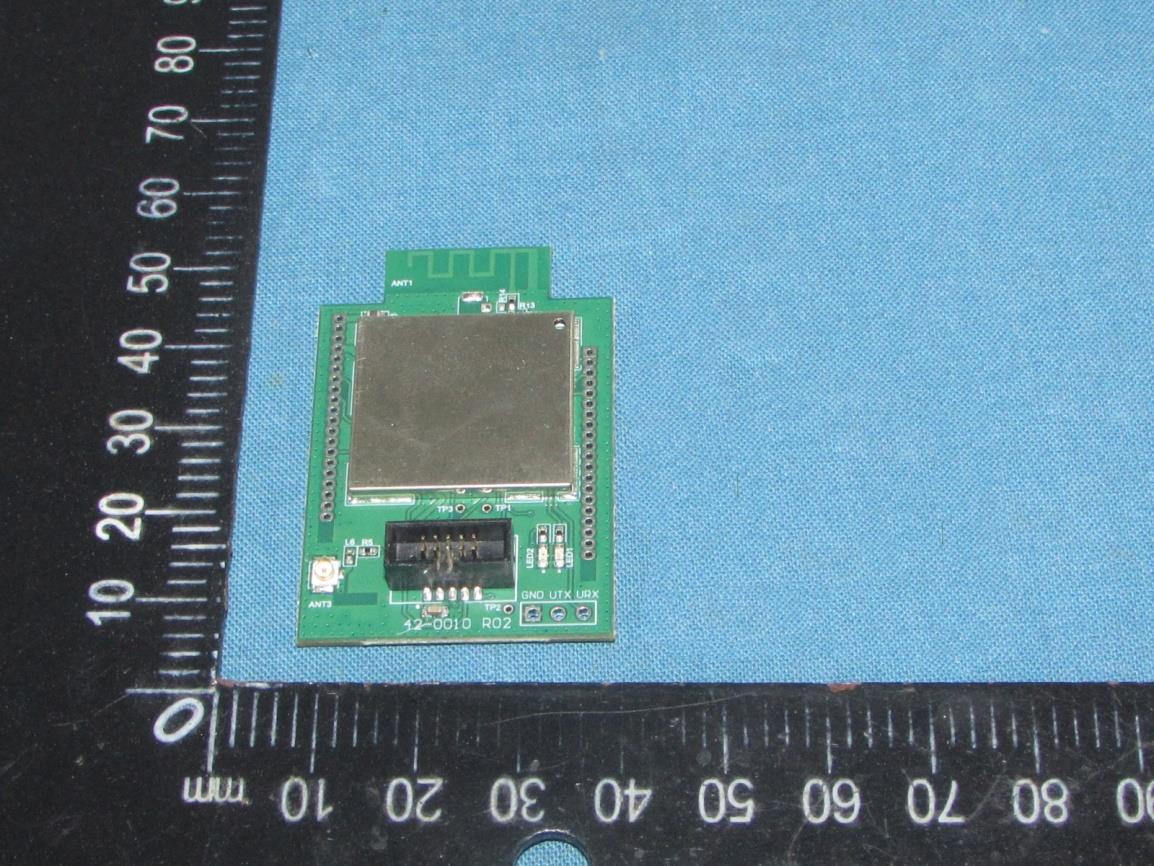
EXHIBIT B - EUT INTERNAL PHOTOGRAPHS Antenna
Bay Area Compliance Laboratories Corp. (Kunshan) Report No.: RSHD200327001-00B FCC Part 15.247 Page 12 of 40 FCC §1.1310& §2.1091 –MAXIMUM PERMISSIBLE EXPOSURE (MPE) Applicable Standard According to subpart §2.1091 and subpart §1.1310, systems operating under the provisions of this section shall be operated in a manner that ensures that the public is not exposed to radio frequency energy level in excess of the Commission’s guidelines. Limits for Maximum Permissible Exposure (MPE) (§1.1310, §2.1091) (B) Limits for General Population/Uncontrolled Exposure Frequency Range (MHz) Electric Field Strength (V/m) Magnetic Field Strength (A/m) Power Density (mW/cm 2 ) Averaging Time (minutes) 0.3-1.34 614 1.63 *(100) 30 1.34-30 824/f 2.19/f *(180/f²) 30 30-300 27.5 0.073 0.2 30 300-1500 / / f/1500 30 1500-100,000 / / 1.0 30 f = frequency in MHz; * = Plane-wave equivalent power density; According to §1.1310 and §2.1091 RF exposure is calculated. Calculated Formulary: Predication of MPE limit at a given distance S = PG/4πR² = power density (in appropriate units, e.g. mW/cm 2 ); P = power input to the antenna (in appropriate units, e.g., mW); G = power gain of the antenna in the direction of interest relative to an isotropic radiator, the power gain factor, is normally numeric gain; R = distance to the center of radiation of the antenna (appropriate units, e.g., cm); Calculated Data: Mode Frequency Range (MHz) Antenna Gain Tune-up Conducted Power Evaluation Distance (cm) Power Density (mW/cm 2 ) MPE Limit (mW/cm 2 ) (dBi) (numeric) (dBm)(mW) Zigbee 2405~24800 1.00 16.0039.81 20 0.0079 1.0 Note: The tune-up Conducted power was declared by the manufacturer. Conclusion: The EUT meets exemption requirement - RF exposure evaluation greater than 20cm distance specified in § 2.1091. If the device built into a host as a portable usage, the additional RF exposure evaluation may be required as specified by§ 2.1093.
Note: This test report is prepared for the customer shown above and for the device described herein. It may not be duplicated or used in part without prior written consent from Bay Area Compliance Laboratories Corp. This report is valid only with a valid digital signature. The digital signature may be available only under the Adobe software above version 7.0. FCC PART 15.247 TEST REPORT For Hefei DappWorks Technology Co. Ltd. Room 611-166, R&D Center Building International Intelligent Voice Industrial Park, 3333 Xiyou Road, High-tech Zone, Hefei, China FCC ID: 2AV5NMSWUP-310 Report Type: Original Report Product Type: EM3587 ZigBee Module Test Engineer: Chris Wan g Re port Number: RSHD200327001-0B Re port Date: 2020-04-30 Reviewed B y: Oscar Ye EMC Manager Prepared By: Bay Area Compliant Laboratories Corp. (Kunshan) No.248 Chenghu Road,Kunshan,Jiangsu province,China Tel: +86-0512-86175000 Fax: +86-0512-88934268 www.baclcorp.com.cn Bay Area Compliance Laboratories Corp. (Kunshan) Report No.: RSHD200327001-00B FCC Part 15.247 Page 2 of 37 TABLE OF CONTENTS GENERAL INFORMATION ....................................................................................................................................... 4 PRODUCT DESCRIPTION FOR EQUIPMENT UNDER TEST (EUT) ..................................................................................... 4 OBJECTIVE ................................................................................................................................................................... 4 RELATED SUBMITTAL(S)/GRANT(S) ............................................................................................................................. 4 TEST METHODOLOGY .................................................................................................................................................. 4 MEASUREMENT UNCERTAINTY .................................................................................................................................... 5 TEST FACILITY ............................................................................................................................................................. 5 SYSTEM TEST CONFIGURATION .......................................................................................................................... 6 DESCRIPTION OF TEST CONFIGURATION ...................................................................................................................... 6 EQUIPMENT MODIFICATIONS ....................................................................................................................................... 6 EUT EXERCISE SOFTWARE .......................................................................................................................................... 6 SUPPORT EQUIPMENT LIST AND DETAILS .................................................................................................................... 7 EXTERNAL I/O CABLE .................................................................................................................................................. 7 BLOCK DIAGRAM OF TEST SETUP ................................................................................................................................ 8 SUMMARY OF TEST RESULTS ............................................................................................................................. 10 TEST EQUIPMENT LIST ......................................................................................................................................... 11 FCC §1.1310& §2.1091 –MAXIMUM PERMISSIBLE EXPOSURE (MPE) ............................................................. 12 CALCULATED FORMULARY: ....................................................................................................................................... 12 FCC §15.203 - ANTENNA REQUIREMENT ........................................................................................................... 13 APPLICABLE STANDARD ............................................................................................................................................ 13 ANTENNA CONNECTOR CONSTRUCTION .................................................................................................................... 13 FCC §15.207 (a) – AC LINE CONDUCTED EMISSIONS ..................................................................................... 14 APPLICABLE STANDARD ............................................................................................................................................ 14 EUT SETUP ................................................................................................................................................................ 14 EMI TEST RECEIVER SETUP ....................................................................................................................................... 14 TEST PROCEDURE ...................................................................................................................................................... 14 CORRECTED FACTOR & OVER LIMIT CALCULATION .................................................................................................. 15 TEST RESULTS SUMMARY .......................................................................................................................................... 15 TEST DATA ................................................................................................................................................................ 15 FCC §15.209, §15.205 & §15.247(d) - SPURIOUS EMISSIONS ............................................................................. 18 APPLICABLE STANDARD ............................................................................................................................................ 18 EUT SETUP ...................................…
Text truncated - open the document above for the full version.
EXHIBIT C - TEST SETUP PHOTOGRAPHS Conducted Emissions (Front View) Conducted Emissions (Side View) Radiated Emissions (Below 1GHz) Radiated Emissions (Above 1GHz)
| # | Rule Parts | Frequency Range | Power Output |
|---|---|---|---|
| 1 | 15C | 2.40 GHz - 2.48 GHz | 36.00 mW |

EFR32 ZigBee Module
Equipment Class
DTS - Digital Transmission System