2AVHCDB-DP11226WONDOM In-circuit Programmer
Sure Electronics Co.,Ltd.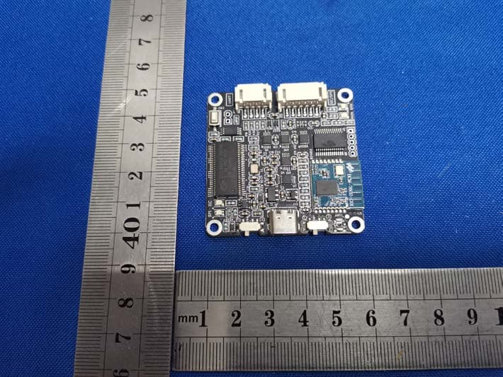
Click to zoom
Application Details
- Equipment Class
- DTS - Digital Transmission System
- Date of Grant
- Aug 17, 2022
- Application Purpose
- Original Equipment
- Date of Application
- Aug 17, 2022
- Equipment Note
- WONDOM In-circuit Programmer
- Frequency Range
- 2402.00000000 - 2480.00000000
- Company
- Sure Electronics Co.,Ltd.
- Country
- China
Documents & Files
Document Text
Text extracted from the exhibit documents filed with the FCC. Open a document above to read the original.
Users Manual
WONDOM ICP5 User Guide IN-CIRCUIT PROGRAMMER FOR PROGRAMMING, APP CONTROL & PC UI -ICP5 BySureElectronicsCo.,Ltd. Video Tutorial Copyright © 2021 Sure Electronics Co., Ltd. Revision History RevisionDescriptionDate V1.0WONDOM ICP5 PCB version –V10010-Sept-2021 V1.01WONDOM ICP5 PCB version –V100 (USB Driver Added)8-Oct-2021 V1.02WONDOM ICP5 PCB version –V100 (PC UI Updated)10-Nov-2021 Copyright © 2021 Sure Electronics Co., Ltd. Overview ICP5 -Multi-Purpose In-Circuit Programmer ForusewithWONDOMproductsintegratedwithDSP,providingvariousfunctionsasprogrammingwithSigmaStudio, APPcontrolandPCUIcontrol.Inaddition,ICP5supportsonlineFirmwareUpgrade.Owingtotheequippedauto- identificationsystem,ICP5canrecognizethetargetproductsautomaticallyoncetheyareconnected. On-board self-boot EEPROM for operating with Analog Devices, Inc., SigmaStudio™ Integrated with Bluetooth BLE for APP control Integrated with USB UART for PC UI Control Update ICP5 by your side for use with more products Copyright © 2021 Sure Electronics Co., Ltd. Applicable Products ModelBrief DescriptionProgrammingAPP ControlPC UI Control APM2ADAU1701 DSP kernel boardYY (End of Jul, 2022)Y (EndofNov) JAB2v22.0 / 0.1 Audio amplifier board with DSP & BT 5.0NNY JAB32.0 / 0.1 Audio amplifier board with ADAU1701 DSPYY (End of Jun, 2022)Y (Mid-Nov) JAB3+ 2.0 / 0.1 Audio amplifier board with ADAU1701 DSP & BT 5.0 YY (End of May, 2022)Y (EndofOct) JAB4 4.0 / 2.1 / 2.0 / 0.2 30W Audio amplifier board with ADAU1701 DSP & BT 5.0 YY (End of Apr, 2022)Y (Mid-Oct) JAB5 4.0 / 2.1 / 2.0 / 0.2 100W Audio amplifier board with ADAU1701 DSP & BT 5.0 YY (End of Mar, 2022)Y (EndofSep) NrepresentsforNOTAVAILABLE;YrepresentsforAVAILABLE. Yinredmeansthatit’sinplanandyoucanseetheestimatedreleasedate. Copyright © 2021 Sure Electronics Co., Ltd. Contents ICP5 IntroductionProgrammingAPP ControlPC UI Control Wecoverthefollowingcontentsinthisdocument.Youcanclickonthetitletoskiptocorrespondingchapter. Intro Introduction of ICP5 Programmer ICP5 IN-CIRCUIT PROGRAMMER FOR SIGMASTUDIO PROGRAMMING, APP CONTROL & PC UI CONTROL Copyright © 2021 Sure Electronics Co., Ltd. Interface Definition Bluetooth BLE With Built-in antenna ExternalBluetoothAntenna SW1MODEFUNCTION ①USBiSigmaStudioProgramming ②RemotePC UI / APP Control SW1 ControlModeSwitch SW4 USBiModeSwitch SW4MODEFUNCTION ①SPI For WONDOM Products with ADAU1452 ②IIC For WONDOM Products with ADAU1701 U1,USBType-CPort 1)DC5Vpowersupply 2)Communicationwithcomputer J1, PH-6Pos Connection Port For connection with WONDOM products integrated with Analog DSP J2, PH-4Pos Connection Port For connection with WONDOM products integrated with other DSP SW3,BootloaderStartSwitch ForICP5firmwareupgrade RUN Power LED indicator ERROR Error LED indicator IICSPI Copyright © 2021 Sure Electronics Co., Ltd. Power Supply A USB Type-C port is used for power of ICP5. In addition to power, this USB port supports communication with the computer for programming or PC UI control after connection. Once ICP5 is connected with target products through the PH-6Pos or PH-4Pos connection port, ICP5 will be powered by the target products directly. There is no need to connect with an extra power supply. U1, DC5V power supply U1 Copyright © 2021 Sure Electronics Co., Ltd. Bluetooth Module ICP5 is integrated with high performance Bluetooth BLE module, which are for APP control with target products. For now, there is no APP available for use with ICP5. We will develop APPs in the near future. Bluetooth BLE Module Copyright © 2021 Sure Electronics Co., Ltd. Connection Port J1, the PH-6Pos-connector, adopting I2C / SPI communication protocol, is used for connection with WONDOM products that are integrated with Analog ADAU1701 DSP and later ADAU1452 DSP. ICP5 is equipped with automatic identification system, which means, it will identify the target product once it is connected. J1, PH-6Pos-Connection Port J1 Copyright © 2021 Sure Electronics Co., Ltd. Connection Port J2, the PH-4Pos-connector, adopting UART communication protocol, is used for connection with WONDOM products integrated with other DSP chips, for now there is only JAB2v2. Since the DSP used is not from Analog, it will not support programming with SigmaStudio. J2, PH-4Pos-Connection Port J2 Copyright © 2021 Sure Electronics Co., Ltd. Control Switch SW1 is a control mode switch between SigmaStudio programming and user interface control (APP control & PC UI control). SW1, Control Mode Switch SW1MODEFUNCTION ①USBiSigmaStudioProgramming ②RemoteAPP Control / PC UI Control If you want SigmaStudioprogramming function, you need to set SW1 at ①“USBi”; IfyouwantAPP/PCUIcontrol,youneedtosetSW1at ②“Remote”. SW1 Copyright © 2021 Sure Electronics Co., Ltd. Firmware Upgrade As mentioned before, besides current products with ADAU1701 DSP, we will develop products with ADAU1452 in future. WONDOM products with ADAU1701 DSP communicates with SigmaStudio via I2C, while products with ADAU1452 plans to communicate with SigmaStudiovia SPI. Therefore, we leave the switch for future use with ADAU1452 products. Therefore, besides setting SW1 at ①“USBi”, we need to set SW4 as well before programming. Set SW4 at ②“IIC” when you want to program products integrated with ADAU1701; Set SW4 at ①“SPI” when you want to program products integrated with ADAU1452. SW4, USBi Mode Switch SW4MODEFUNCTION ①SPI For WONDOM Products with ADAU1452 ②IIC For WONDOM Products with ADAU1701 SW4 Copyright © 2021 Sure Electronics Co., Ltd. Firmware Upgrade SW3 is a Bootloader start switch, which is provided to upgrade the firmware program on the ICP5 so that it can be used with various DSP products. ICP5 needs online firmware upgrade if it’s used with a target product for the first time. As for the details, please refer to “Firmware Update” part. SW3, Firmware upgrade switch SW3 Copyright © 2021 Sure Electronics Co., Ltd. LED Indicator When power on, this indicator will be ON in green; When power off, this indicator will be OFF; When ICP5 is in BootLoaderm…
Text truncated - open the document above for the full version.
Cover Letter(s)
Sure Electronics Co.,Ltd. Agent Authorization Company: Sure Electronics Co.,Ltd. Address: 3F,Building F6,No.9,Weidi Road,Qixia Dist.,Nanjing,China Product Name: WONDOM In-circuit Programmer Model Number(s): DB-DP11226, DB-DP11224, DB-DP11219 Product Description: WONDOM In-circuit Programmer We authorize MiCOM Labs Inc., 575 Boulder Court, Pleasanton, California 94566, USA, to act on our behalf on all matters concerning the certification of above named equipment. We declare that MiCOM Labs Inc. is allowed to forward all information related to the approval and certification of equipment to the regulatory agencies as required and to discuss any issues concerning the approval application. Any and all acts carried out by MiCOM Labs on our behalf shall have the same effect as acts of our own. Signature: Date: 2022-08-11 Name: Johnson Zhang Title: engineer Company: Sure Electronics Co.,Ltd.
Cover Letter(s)
Sure Electronics Co.,Ltd. FCC Modular Approval Request Rev 3.0 Federal Communications Commission Equipment Authorization Division 7435 Oakland Mills Road Columbia, MD 21046 USA Date: 2022.08.11 Subject; WONDOM In-circuit Programmer Company name: Sure Electronics Co.,Ltd. FCC ID: 2AVHCDB-DP11226 Dear Sir/Madam, This letter includes the FCC application requirements for Modular Transmitter Approval Request for;- FCC KDB 996369 D01 ‘Module Certification Guide v02; and FCC KDB 996369 D03 OEM Manual v01 In accordance with 47CFR 15.212 Modular Transmitters and KDB 996369 D01 ‘Module Equip Auth Guide v02’. FCC ID: 2AVHCDB-DP11226 has been examined against the following requirements. Requirement per 15.212 and KDB 996369 D01 Explanation from Grantee (do not write yes/no, but explain why product complies/how it is achieved) The radio elements must have the radio frequency circuitry shielded. Physical components and tuning capacitor(s) may be located external to the shield, but must be on the module assembly. The module has no shield cover The module must have buffered modulation/data inputs to ensure that the device will comply with Part 15 requirements with any type of input signal. All modulation and data inputs are buffered by circuitry on the transmitter chip HW3000RF, as is shown in the schematic. The module must contain power supply regulation on the module. Power supply regulation is provided by circuitry on the transmitter chip HW3000RF, as is shown in the schematic. The module must contain a permanently attached antenna, or contain a unique antenna connector, and be marketed and operated only with specific antenna(s), per §§ 15.203, 15.204(b), 15.204(c), 15.212(a), 2.929(b). The module contain a permanently attached antenna and spurious emission have been fulfilled. Please reference the exhibition Test Report. The module must demonstrate compliance in a stand-alone configuration. Please reference exhibition Test Configuration Photo for the stand-alone test configuration. The module must be labeled with its permanently affixed FCC ID label, or use an electronic display (see KDB Publication 784748). The instruction on the labelling rule of the end product has been stated in the Users manual of this module. Please also see the exhibition Label Sample. The module must comply with all specific rules applicable to the transmitter, including all the conditions provided in the integration instructions by the grantee. The required FCC rule has been fulfilled and all the instructions for maintaining compliance has been clearly stated in the Users Manual. The module must comply with RF exposure requirements Please refer exhibition RF Exposure for the compliance of MPE RF exposure rule. Sure Electronics Co.,Ltd. FCC Modular Approval Request Rev 3.0 Integration Instructions for host product manufacturers The following items are submitted in support of application for Modular Transmitter FCC ID as noted above as required by the FCC KDB 996369 D03 OEM Manual v01. These items are provided as integration instructions for host product manufacturers (e.g., OEM instruction manual) to use when integrating a module in a host product. Any requirements that are not applicable to the Module are as indicated below. Summary of requirements and Checklist. Refer to the KDB for description of the complete requirements; KDB Ref Sect Requirements of KDB 996369 D03 User Manual Page Number reference 2.2 List of applicable FCC rules 50 2.3 Summarize the specific operational use conditions 50 2.4 Limited module procedures 50 2.5 Trace antenna designs 50 2.6 RF exposure considerations 51 2.7 Antennas 51 2.8 Label and compliance information 52 2.9 Information on test modes and additional testing requirements 52 2.10 Additional testing, Part 15 Subpart B disclaimer 52 Name: Johnson Zhang Date: 2022.08.11 Title: engineer Signature of applicant
Cover Letter(s)
Sure Electronics Co.,Ltd. Office of Engineering Technology Federal Communications Commission 7435 Oakland Mills Road Columbia, MD 21046 USA Date: 2022/08/11 Subject; Request for Confidentiality FCC ID: 2AVHCDB-DP11226 To Whom It May Concern, Pursuant to the provisions of the Commission’s rules Title 47 Sections §0.457 and §0.459, we are requesting the Commission to withhold the following attachment(s) as confidential documents from public disclosure indefinitely. These documents contain detailed system and equipment descriptions and are considered as proprietary information in operation of the equipment. The public disclosure of these documents might be harmful to our company and would give competitors an unfair advantage in the market. Schematic Diagram Block Diagram Operational Description In additional to above mentioned documents, in order to comply with the marketing regulations in Title 47 CFR §2.803 and the importation rules in Title 47 CFR §2.1204, while ensuring that business sensitive information remains confidential until the actual marketing of newly authorized devices, we request Short Term Confidentiality of the following attachment(s); User Manual For 45 days, pursuant to Public Notice DA 04-1705. OR For 180 days pursuantto KDB 726920 D01. It is our understanding that all measurement test reports, FCC ID label format and correspondence during the certification review process cannot be granted as confidential documents and this information will be available for public review once the grant of equipment authorization is issued. Sincerely, Signature: Name: Johnson Zhang Title: engineer
Cover Letter(s)
Sure Electronics Co.,Ltd. Model Difference Data:2022.08. 11 Product description: WONDOM In-circuit Programmer Model name: DB-DP11226, DB-DP11224, DB-DP11219 Trade Name: FCC ID: 2AVHCDB-DP11226 All the model are the same circuit and RF module, except model names . Regards Sincerely Client’s signature : Client’s name / title : Johnson Zhang(engineer) Contact information / address:3F,Building F6,No.9,Weidi Road,Qixia Dist.,Nanjing,China
External Photos
External Photos
ID Label/Location Info
Model: DB-DP11226 FCC ID: 2AVHCDB-DP11226 Label Location
Internal Photos
Internal Photos ANT
RF Exposure Info
FCC §15.247 (i), §2.1091 – RF Exposure FCC ID: 2AVHCDB-DP11226 Applied procedures / limit According to FCC §15.247(i) and §1.1307(b)(1), systems operating under the provisions of this section shall be operated in a manner that ensures that the public is not exposed to radio frequency energy level in excess of the Commission’s guidelines. Limits for Occupational / Controlled Exposure Frequency Range (MHz) Electric Field Strength (E) (V/m) Magnetic Field Strength (H) (A/m) Power Density (S) (mW/ cm 2 ) Averaging Time |E| 2 ,|H| 2 or S (minutes) 0.3-3.0 614 1.63 (100)* 6 3.0-30 1842 / f 4.89 / f (900 / f)* 6 30-300 61.4 0.163 1.0 6 300-1500 F/300 6 1500-100,000 5 6 Note: ƒ is frequency in MHz * = Power density limit is applicable at frequencies greater than 100 MHz Limits for General Population / Uncontrolled Exposure Frequency Range (MHz) Electric Field Strength (E) (V/m) Magnetic Field Strength (H) (A/m) Power Density (S) (mW/ cm 2 ) Averaging Time |E| 2 ,|H| 2 or S (minutes) 0.3-1.34 614 1.63 (100)* 30 1.34-30 824/f 2.19/f (180/f)* 30 30-300 27.5 0.073 0.2 30 300-1500 F/1500 30 1500-100,000 1.0 30 Note: f = frequency in MHz * = Plane-wave equivalent power density MPE PREDICTION Predication of MPE limit at a given distance, Equation from OET Bulletin 65, Edition 97-01 Where: S = power density P = power input to antenna G = power gain of the antenna in the direction of interest relative to an isotropic radiator R = distance to the center of radiation of the antenna,R=20cm Test Result of RF Exposure Evaluation Modes& Channel Freq. (MHz) Tune up Produce power Maximu m peak output power (dBm) Output power to antenna (mW) Antenna Gain (numeric) Power Density (S) (mW/ cm2) Limit (mW / cm2 ) Result BLE GFSK & LCH 0±1 1 1.2589 1.2589 (1dBi) 0.0003 1 Pass
Test Report
Shenzhen CTB Testing Technology Co., Ltd. Report No.: CTB220729013RFX Report Tel: 4008-707-283Web: http://www.ctb-lab.net Page 1 of 36 TEST REPORT Compiled by: Reviewed by: Approved by: Chen Zheng Arron Liu Bin Mei / Director Note: If there is any objection to the inspection results in this report, please submit a written report to the company within 15 days from the date of receiving the report. The test report is effective only with both signature and specialized stamp. This result(s) shown in this report refer only to the sample(s) tested. Without written approval of Shenzhen CTB Testing Technology Co., Ltd. this report can’t be reproduced except in full. The tested sample(s) and the sample information are provided by the client. “*” indicates the testing items were fulfilled by subcontracted lab. “#” indicates the items are not in CNAS accreditation scope. Product Name: WONDOM In-circuit Programmer FCC ID: 2AVHCDB-DP11226 Trademark: Model Number: DB-DP11226, DB-DP11224, DB-DP11219 Prepared For: Sure Electronics Co., Ltd. Address: 3 F, Building F6 ,No.9, Weidi Road, Qixia Dist., Nanjing, China Manufacturer: Sure Electronics Co., Ltd. Address: 3 F, Building F6, No.9, Weidi Road, Qixia Dist., Nanjing, China Prepared By: Shenzhen CTB Testing Technology Co., Ltd. Address: Floor 1&2, Building A, No. 26 of Xinhe Road, Xinqiao Community, Xinqiao Street, Baoan District, Shenzhen, Guangdong, China. Sample Received Date: Jul. 21, 2022 Sample tested Date: Jul. 21, 2022 to Jul. 29, 2022 Issue Date: Jul. 29, 2022 Report No.: CTB220729013RFX Te s t Standards FCC Part15.247 ANSI C63.10:2013 Test Results PASS Remark: This is Bluetooth radio test report. Shenzhen CTB Testing Technology Co., Ltd. Report No.: CTB220729013RFX Report Tel: 4008-707-283 Web: http://www.ctb-lab.net Page 2 of 36 TABLE OF CONTENT Test Report Declaration Page 1. VERSION ........................................................................................................................................ 3 2. TEST SUMMARY ........................................................................................................................... 4 3. MEASUREMENT UNCERTAINTY ................................................................................................. 5 4. PRODUCT INFORMATION AND TEST SETUP ............................................................................ 6 4.1 Product Information .......................................................................................................................... 6 4.2 Test Setup Configuration .................................................................................................................. 6 4.3 Support Equipment........................................................................................................................... 6 4.4 Channel List ..................................................................................................................................... 7 4.5 Test Mode ........................................................................................................................................ 7 4.6 Test Environment ............................................................................................................................. 7 5. TEST FACILITY AND TEST INSTRUMENT USED ....................................................................... 8 5.1 Test Facility ...................................................................................................................................... 8 5.2 Test Instrument Used ....................................................................................................................... 8 6. AC POWER LINE CONDUCTED EMISSION .................................................................................. 11 6.1 Block Diagram Of Test Setup ......................................................................................................... 11 6.2 Limit ................................................................................................................................................ 11 6.3 Test procedure ............................................................................................................................... 11 6.4 Test Result ..................................................................................................................................... 13 7. RADIATED SPURIOUS EMISSION ............................................................................................. 15 7.1 Block Diagram Of Test Setup ......................................................................................................... 15 7.2 Limit ................................................................................................................................................ 15 7.3 Test procedure ............................................................................................................................... 16 7.4 Test Result ..................................................................................................................................... 17 8. BAND EDGE AND RF COUNDUCTED SPURIOUS EMISSIONS ............................................... 24 8.1 Block Diagram Of Test Setup ......................................................................................................... 24 8.2 Limit ................................................................................................................................................ 24 8.3 Test procedure ............................................................................................................................... 24 8.4 Test Result ..................................................................................................................................... 25 9. COUDUCTED OUTPUT POWER ................................................................................................. 27 9.1 Block Diagr…
Text truncated - open the document above for the full version.
Test Setup Photos
Radiated Emission Below 1G Above 1GHz Conducted Emission
Contact Information
Applicant
Johnson Zhang
Technical Contact
Test Firm
Shenzhen CTB Testing Technology Co., Ltd.Rita Xiao
[email protected]86-13538218145
Technical Specifications
| # | Rule Parts | Frequency Range | Power Output |
|---|---|---|---|
| 1 | 15C | 2.40 GHz - 2.48 GHz | 930.00 µW |
Other Applications from Sure Electronics Co.,Ltd.
2AVHC-JAB6
Apr 16, 2026Class D Audio Amplifier Board w ADAU1701 DSP Bluetooth Ver5.0, Supporting TWS, I2S, Line input - TPA3255 JAB6
Equipment Class
DSS - Part 15 Spread Spectrum Transmitter
2AVHC-BDM8
Mar 31, 2026300W+300W DSP PC UI TPA3255 Bluetooth 5.3 Audio Amplifier DC18-48V AUX input Volume Control BDM8 Audio Amplifier Board
Equipment Class
DTS - Digital Transmission System
2AVHC-OEM-05146
Jan 08, 2020Bluetooth Audio Amplifier Board
Equipment Class
DSS - Part 15 Spread Spectrum Transmitter