2AWIA-DSJTSP26A14G Body Worn Camera
Anhui Tsinglink Information Technology Co., Ltd.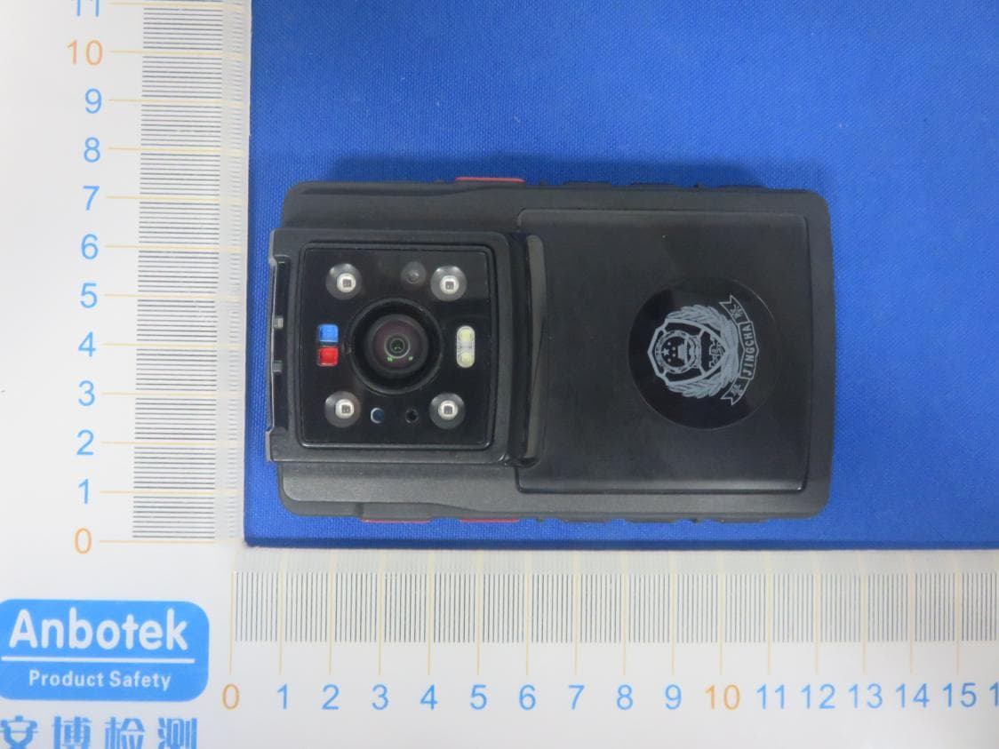
Click to zoom
Application Details
- Equipment Class
- PCB - PCS Licensed Transmitter
- Date of Grant
- Jul 07, 2020
- Application Purpose
- Original Equipment
- Date of Application
- Jul 07, 2020
- Equipment Note
- 4G Body Worn Camera
- Frequency Range
- 2565.00000000 - 2645.00000000
- Country
- China
Documents & Files
Document Text
Text extracted from the exhibit documents filed with the FCC. Open a document above to read the original.
Users Manual
4G Body Worn Camera USER MANUAL Model: DSJ-TSP26A1 1 Thank you very much for purchasing our product. If you have any questions or needs, please feel free to contact us This manual is suitable for DSJ-TSP26A1 body worn camera. This manual may contain technical inaccuracies, inconsistencies with product functions and operations, or misprints. We will update the contents of this manual according to the enhancement of product functions, and will regularly improve or update the products or procedures described in this manual. The updated content will be added in the new version of this manual without prior notice. In order to make the user of this product to easily master the installation and use method, this product manual is specially made for their reference. Please read this manual carefully before installation and use. Precautions For Safe Use 4G body worn camera is a specially customized precision electronic device. In order to avoid improper operation during the use of the terminal, which may lead to damages, please pay attention to the following matters during the use: In case of terminal failure, please do not disassemble or repair the terminal arbitrarily. Please hand the terminal to our professional staff for maintenance; Please use the specified power adapter to charge the terminal. Do not use the power adapter higher than the rated voltage. Otherwise the terminal may be damaged; When the terminal is not used for a long time, the battery should be taken out; please fully charge the battery before using it again; Please use specified battery; wrong battery will have the risk of explosion, follow the instructions to dispose of the used battery; Do not short-circuit, decompose or throw the battery into fire; The terminal shall not be dismantled or transformed without authorization; Avoid exposing the screen and lens to direct sunlight; keep away from moisture and water. 2 FCC Statement : This device complies with Part 15 of the FCC Rules. Operation is subject to the following two conditions: (1) This device may not cause harmful interference, and (2) This device must accept any interference received, including interference that may cause undesired operation. Warning: Changes or modifications not expressly approved by the party responsible for compliance could void the user's authority to operate the equipment. NOTE: This equipment has been tested and found to comply with the limits for a Class B digital device, pursuant to Part 15 of the FCC Rules. These limits are designed to provide reasonable protection against harmful interference in a residential installation. This equipment generates uses and can radiate radio frequency energy and, if not installed and used in accordance with the instructions, may cause harmful interference to radio communications. However, there is no guarantee that interference will not occur in a particular installation. If this equipment does cause harmful interference to radio or television reception, which can be determined by turning the equipment off and on, the user is encouraged to try to correct the interference by one or more of the following measures: Reorient or relocate the receiving antenna. Increase the separation between the equipment and receiver. Connect the equipment into an outlet on a circuit different from that to which the receiver is connected. Consult the dealer or an experienced radio/TV technician for help. RF Warning statement: The device has been evaluated to meet general RF exposure requirement. The device can be used in portable exposure condition without restriction. 3 Content 1. Product introduction ............................................................................................................ 4 2. Structural sketch .................................................................................................................... 5 2.1 Product appearance ....................................................................................................... 5 2.2 Button and indicator light introduction .................................................................... 6 2.3 Accessories interface ...................................................................................................... 7 2.4 Insert and take out Naso-SIM card,TF card ............................................................. 8 2.5 Back clamp installation and removel ....................................................................... 10 3. Quick login guide ................................................................................................................ 11 3.1 Quick login ...................................................................................................................... 10 3.2 Main interface ................................................................................................................ 11 3.3【Setting】interface ...................................................................................................... 12 3.4【Recording】interface................................................................................................. 13 3.5【Logout】interface ...................................................................................................... 13 3.6【Files management】interface ................................................................................. 13 3.7【Cluster】interface ....................................................................................................... 13 3.8 【Talk&Talkback】interface ...................................................................................... 13 4. Technical parameters ......................................................................................................... 14 5. Common troubleshooting list .......................................................................................... 15 4 1. Product introduction 4G HD body worn camera DSJ-TSP26A1 is a police law enforcement integrat…
Text truncated - open the document above for the full version.
Cover Letter(s)
Anhui Tsinglink Information Technology Co., Ltd. Declaration on Model Differences We, Anhui Tsinglink Information Technology Co., Ltd. 17-18/F, Block A Building J1, Innovation Industry Park Phase 2, High-tech Zone, Hefei, China. Declare that the following product(s): Product Name:4G Body Worn Camera Model No.:DSJ-TSP26A1, DSJ-TSP FCC ID: 2AWIA-DSJTSP26A1 Utilize the identical circuit design, PCB layout, shielding and interface with(DSJ-TSP26A1), only the model appearance are different. Therefore this application can be regarded as identical in performance to the submitted test sample. The manufacturer would take all the responsibilities for the above product(s). For and on behalf of Hefei, China Authorized personLocation Name:Zhang Liu Position:Overseas Sales Director Date of issue:2020-06-23 *I hereby declare that I am entitled to sign on behalf of the applicant and that the information supplied is correct and complete.
Cover Letter(s)
Anhui Tsinglink Information Technology Co., Ltd. Office of Engineering Technology Federal Communications Commission 7435 Oakland Mills Road Columbia, MD 21046 USA Date: 2019/12/16 Subject; Request for Confidentiality FCC ID: 2AWIA-DSJTSP26A1 To Whom It May Concern, Pursuant to the provisions of the Commission’s rules Title 47 Sections §0.457 and §0.459, we are requesting the Commission to withhold the following attachment(s) as confidential documents from public disclosure indefinitely. These documents contain detailed system and equipment descriptions and are considered as proprietary information in operation of the equipment. The public disclosure of these documents might be harmful to our company and would give competitors an unfair advantage in the market. Schematic Diagram Block Diagram Parts List Operational Description FCC SW SECURITY DESCRIPTION Tune up In additional to above mentioned documents, in order to comply with the marketing regulations in Title 47 CFR §2.803 and the importation rules in Title 47 CFR §2.1204, while ensuring that business sensitive information remains confidential until the actual marketing of newly authorized devices, we request Short Term Confidentiality of the following attachment(s); External Photos Test Setup Photos Internal Photos User Manual For 45 days, pursuant to Public Notice DA 04-1705. OR For 180 days pursuant to KDB 726920 D01. It is our understanding that all measurement test reports, FCC ID label format and correspondence during the certification review process cannot be granted as confidential documents and this information will be available for public review once the grant of equipment authorization is issued. Sincerely, Signature: Name:Zhang Liu Anhui Tsinglink Information Technology Co., Ltd. Title: Overseas Sales Director
Cover Letter(s)
Anhui Tsinglink Information Technology Co., Ltd. Letter of Authorization Company: Anhui Tsinglink Information Technology Co., Ltd. Address: 17-18/F, Block A Building J1, Innovation Industry Park Phase 2, High- tech Zone, Hefei, China. Product Name: 4G Body Worn Camera Model Number(s): DSJ-TSP26A1, DSJ-TSP Product Description: 4G Body Worn Camera We authorize MiCOM Labs Inc., 575 Boulder Court, Pleasanton, California 94566, USA, to act on our behalf on all matters concerning the certification of above named equipment. We declare that MiCOM Labs Inc. is allowed to forward all information related to the approval and certification of equipment to the regulatory agencies as required and to discuss any issues concerning the approval application. Any and all acts carried out by MiCOM Labs on our behalf shall have the same effect as acts of our own. Signature: Date: 23/06/2020 Name:Zhang Liu Title:Overseas Sales Director Company: Anhui Tsinglink Information Technology Co., Ltd.
External Photos
Model Number: DSJ-TSP26A1
ID Label/Location Info
Label Location:
ID Label/Location Info
Product Name: 4G Body Worn Camera Model No.: DSJ-TSP26A1 FCC ID: 2AWIA-DSJTSP26A1 This device complies with Part 15 of the FCC Rules. Operation is subject to the following two conditions: (1) This device may not cause harmful interference, and (2) This device must accept any interference received, including interference that may cause undesired operation.
Internal Photos
Model Number: DSJ-TSP26A1 NFCANT BT&WiFiANT LTEANT
RF Exposure Info
Report No.:18220WC00047608FCC ID:2AWIA-DSJTSP26A1 Page 1 of 131 FCC SAR Test Report Client Name:Anhui Tsinglink Information Technology Co., Ltd. Address: 17-18/F, Block A Building J1, Innovation Industry Park Phase 2, High-tech Zone, Hefei, China. Product Name:4G Body Worn Camera Date: Jun. 16, 2020 Shenzhen Anbotek Compliance Laboratory Limited Report No.:18220WC00047608FCC ID:2AWIA-DSJTSP26A1 Page 2 of 131 Contents 1. Statement of Compliance .............................................................................................................. 6 2. General Information ........................................................................................................................ 7 2.1Client Information .......................................................................................................................................................................... 7 2.2Description of Equipment Under Test (EUT) ............................................................................................................................ 7 2.3Device Category and SAR Limits ............................................................................................................................................... 9 2.4Applied Standard ........................................................................................................................................................................... 9 2.5Environment of Test Site .............................................................................................................................................................. 9 2.6Test Configuration ......................................................................................................................................................................... 9 3. Specific Absorption Rate (SAR) ................................................................................................. 10 3.1Introduction ................................................................................................................................................................................... 10 3.2SAR Definition .............................................................................................................................................................................. 10 4. SAR Measurement System ......................................................................................................... 11 4.1E-Field Probe ............................................................................................................................................................................... 12 4.2Data Acquisition Electronics (DAE) ......................................................................................................................................... 12 4.3Robot ............................................................................................................................................................................................. 13 4.4Measurement Server .................................................................................................................................................................. 14 4.5Phantom ........................................................................................................................................................................................ 14 4.6Device Holder .............................................................................................................................................................................. 16 4.7Data Storage and Evaluation .................................................................................................................................................... 17 5. Test Equipment List ...................................................................................................................... 19 6. Tissue Simulating Liquids ............................................................................................................ 21 7. System Verification Procedures ................................................................................................. 23 8. EUT Testing Position ................................................................................................................... 25 8.1Body Worn Position .................................................................................................................................................................... 25 9. Measurement Procedures ........................................................................................................... 26 9.1Spatial Peak SAR Evaluation ................................................................................................................................................... 26 9.2Power Reference Measurement .............................................................................................................................................. 27 9.3Area Scan Procedures ............................................................................................................................................................... 27 9.4Zoom Scan Procedures ............................................................................................................................................................. 28 9.5Volume Scan Procedures .......................................................................................................................................................... 29 9.6Power Drift Monitoring ................................................................................................................................................................ 29 10. Conducted Power ....................................................................................................................... 30 11. Antenna Location...…
Text truncated - open the document above for the full version.
Test Report
Report No.: 18220WC00047605FCC ID: 2AWIA-DSJTSP26A1Page 1 of 236 FCC TEST REPORT Client Name: Anhui Tsinglink Information Technology Co., Ltd. Address: 17-18/F, Block A Building J1, Innovation Industry Park Phase 2, High-tech Zone, Hefei, China. Product Name: 4G Body Worn Camera Date: Jun. 16, 2020 Shenzhen Anbotek Compliance Laboratory Limited Report No.: 18220WC00047605FCC ID: 2AWIA-DSJTSP26A1Page 2 of 236 Contents 1. General Information ............................................................................................................................................... 5 1.1. Client Information ....................................................................................................................................... 5 1.2. Description of Device (EUT) ..................................................................................................................... 5 1.3. Auxiliary Equipment Used During Test ................................................................................................... 6 1.4. Description of Test Modes ........................................................................................................................ 6 1.5. Description Of Test Setup ......................................................................................................................... 7 1.6. Test Equipment List .................................................................................................................................... 9 1.7. Measurement Uncertainty ....................................................................................................................... 10 1.8. Description of Test Facility ...................................................................................................................... 10 2. Summary of Test .................................................................................................................................................. 11 2.1. Summary of test result ............................................................................................................................ 11 2.2. Test mode .................................................................................................................................................. 11 3. RF Output Power Test ......................................................................................................................................... 13 3.1. Test Standard and Limit .......................................................................................................................... 13 3.2. Test Setup .................................................................................................................................................. 13 3.3. Test Procedure .......................................................................................................................................... 13 3.4. Test Data .................................................................................................................................................... 13 4. Peak-Average Ratio ............................................................................................................................................ 34 4.1. Test Standard and Limit .......................................................................................................................... 34 4.2. Test Setup .................................................................................................................................................. 34 4.3. Test Procedure .......................................................................................................................................... 34 4.4. Test Data .................................................................................................................................................... 34 5. Modulation Characteristic ................................................................................................................................... 79 6. Occupied Bandwidth ........................................................................................................................................... 80 6.1. Test Standard and Limit .......................................................................................................................... 80 6.2. Test Setup .................................................................................................................................................. 80 6.3. Test Procedure .......................................................................................................................................... 80 6.4. Test Data .................................................................................................................................................... 80 7. Spurious Emissions at Antenna Terminals .................................................................................................... 105 7.1. Test Standard and Limit ........................................................................................................................ 105 7.2. Test Setup ................................................................................................................................................ 105 7.3. Test Procedure ........................................................................................................................................ 105 7.4. Test Data .................................................................................................................................................. 105 8. Spurious Radiated Emissions ......................................................................................................................... 205 8.1. Test Standard and Limit ..............................................................................................…
Text truncated - open the document above for the full version.
Test Report
Report No.: 18220WC00047605FCC ID: 2AWIA-DSJTSP26A1Page 61 of 236 Band2‐20MHz‐16QAM‐18700‐100RB#0 Band2‐20MHz‐16QAM‐18900‐1RB#0 Band2‐20MHz‐16QAM‐18900‐100RB#0 Report No.: 18220WC00047605FCC ID: 2AWIA-DSJTSP26A1Page 62 of 236 Band2‐20MHz‐16QAM‐19100‐1RB#0 Band2‐20MHz‐16QAM‐19100‐100RB#0 Band41‐5MHz‐QPSK‐40265‐1RB#0 Report No.: 18220WC00047605FCC ID: 2AWIA-DSJTSP26A1Page 63 of 236 Band41‐5MHz‐QPSK‐40265‐25RB#0 Band41‐5MHz‐QPSK‐40690‐1RB#0 Band41‐5MHz‐QPSK‐40690‐25RB#0 Report No.: 18220WC00047605FCC ID: 2AWIA-DSJTSP26A1Page 64 of 236 Band41‐5MHz‐QPSK‐41215‐1RB#0 Band41‐5MHz‐QPSK‐41215‐25RB#0 Band41‐5MHz‐16QAM‐40265‐1RB#0 Report No.: 18220WC00047605FCC ID: 2AWIA-DSJTSP26A1Page 65 of 236 Band41‐5MHz‐16QAM‐40265‐25RB#0 Band41‐5MHz‐16QAM‐40690‐1RB#0 Band41‐5MHz‐16QAM‐40690‐25RB#0 Report No.: 18220WC00047605FCC ID: 2AWIA-DSJTSP26A1Page 66 of 236 Band41‐5MHz‐16QAM‐41215‐1RB#0 Band41‐5MHz‐16QAM‐41215‐25RB#0 Band41‐10MHz‐QPSK‐40290‐1RB#0 Report No.: 18220WC00047605FCC ID: 2AWIA-DSJTSP26A1Page 67 of 236 Band41‐10MHz‐QPSK‐40290‐50RB#0 Band41‐10MHz‐QPSK‐40690‐1RB#0 Band41‐10MHz‐QPSK‐40690‐50RB#0 Report No.: 18220WC00047605FCC ID: 2AWIA-DSJTSP26A1Page 68 of 236 Band41‐10MHz‐QPSK‐41190‐1RB#0 Band41‐10MHz‐QPSK‐41190‐50RB#0 Band41‐10MHz‐16QAM‐40290‐1RB#0 Report No.: 18220WC00047605FCC ID: 2AWIA-DSJTSP26A1Page 69 of 236 Band41‐10MHz‐16QAM‐40290‐50RB#0 Band41‐10MHz‐16QAM‐40690‐1RB#0 Band41‐10MHz‐16QAM‐40690‐50RB#0 Report No.: 18220WC00047605FCC ID: 2AWIA-DSJTSP26A1Page 70 of 236 Band41‐10MHz‐16QAM‐41190‐1RB#0 Band41‐10MHz‐16QAM‐41190‐50RB#0 Band41‐15MHz‐QPSK‐40315‐1RB#0 Report No.: 18220WC00047605FCC ID: 2AWIA-DSJTSP26A1Page 71 of 236 Band41‐15MHz‐QPSK‐40315‐75RB#0 Band41‐15MHz‐QPSK‐40690‐1RB#0 Band41‐15MHz‐QPSK‐40690‐75RB#0 Report No.: 18220WC00047605FCC ID: 2AWIA-DSJTSP26A1Page 72 of 236 Band41‐15MHz‐QPSK‐41165‐1RB#0 Band41‐15MHz‐QPSK‐41165‐75RB#0 Band41‐15MHz‐16QAM‐40315‐1RB#0 Report No.: 18220WC00047605FCC ID: 2AWIA-DSJTSP26A1Page 73 of 236 Band41‐15MHz‐16QAM‐40315‐75RB#0 Band41‐15MHz‐16QAM‐40690‐1RB#0 Band41‐15MHz‐16QAM‐40690‐75RB#0 Report No.: 18220WC00047605FCC ID: 2AWIA-DSJTSP26A1Page 74 of 236 Band41‐15MHz‐16QAM‐41165‐1RB#0 Band41‐15MHz‐16QAM‐41165‐75RB#0 Band41‐20MHz‐QPSK‐40340‐1RB#0 Report No.: 18220WC00047605FCC ID: 2AWIA-DSJTSP26A1Page 75 of 236 Band41‐20MHz‐QPSK‐40340‐100RB#0 Band41‐20MHz‐QPSK‐40690‐1RB#0 Band41‐20MHz‐QPSK‐40690‐100RB#0 Report No.: 18220WC00047605FCC ID: 2AWIA-DSJTSP26A1Page 76 of 236 Band41‐20MHz‐QPSK‐41140‐1RB#0 Band41‐20MHz‐QPSK‐41140‐100RB#0 Band41‐20MHz‐16QAM‐40340‐1RB#0 Report No.: 18220WC00047605FCC ID: 2AWIA-DSJTSP26A1Page 77 of 236 Band41‐20MHz‐16QAM‐40340‐100RB#0 Band41‐20MHz‐16QAM‐40690‐1RB#0 Band41‐20MHz‐16QAM‐40690‐100RB#0 Report No.: 18220WC00047605FCC ID: 2AWIA-DSJTSP26A1Page 78 of 236 Band41‐20MHz‐16QAM‐41140‐1RB#0 Band41‐20MHz‐16QAM‐41140‐100RB#0 Report No.: 18220WC00047605FCC ID: 2AWIA-DSJTSP26A1Page 79 of 236 5. Modulation Characteristic According to FCC § 2.1047(d), Part 22H, Part 24E& Part 27 there is no specific requirement for digital modulation, therefore modulation characteristic is not presented. Report No.: 18220WC00047605FCC ID: 2AWIA-DSJTSP26A1Page 80 of 236 6. Occupied Bandwidth 6.1. Test Standard and Limit SpecItemRequirement §2.1049, §22.917, §22.905 §24.238 §27.53(a) a)99% Occupied Bandwidth(kHz) b)26 dB Bandwidth(kHz) 6.2. Test Setup 6.3. Test Procedure 1. The EUT’s output RF connector was connected with a short cable to the spectrum analyzer 2. RBWwas set to about 1% of emission BW, VBW= 3 times RBW. 3. -26dBc display line was placed on the screen (or 99% bandwidth), the occupied bandwidth isthe delta frequency between the two points where the display line intersects the signal trace. 6.4. Test Data EUT Spectrum Analyzer Base Station Report No.: 18220WC00047605FCC ID: 2AWIA-DSJTSP26A1Page 81 of 236 WCDMA Mode: BandChannel Occupied Bandwidth (kHz) 26dB Bandwidth (kHz) Verdict Band II 92624166.54710 PASS Band II 94004171.34718 PASS Band II 95384166.04700 PASS Band V 41324151.74698 PASS Band V 41824156.14693 PASS Band V 42334177.74702 PASS LTE Mode: Band Bandwidt h ModulationChannel RB Configuration Occupied Bandwidth (MHz) 26dB Bandwidth (MHz) Verdict Band21.4MHzQPSK186076RB#01.08821.235PASS Band21.4MHzQPSK189006RB#01.09071.264PASS Band21.4MHzQPSK191936RB#01.08821.232PASS Band21.4MHz 16QAM 186076RB#01.08881.253PASS Band21.4MHz 16QAM 189006RB#01.08781.251PASS Band21.4MHz 16QAM 191936RB#01.08791.266PASS Band23MHzQPSK1861515RB#02.69032.859PASS Band23MHzQPSK1890015RB#02.69132.857PASS Band23MHzQPSK1918515RB#02.67932.867PASS Band23MHz16QAM 1861515RB#02.68542.852PASS Band23MHz16QAM 1890015RB#02.68902.857PASS Band23MHz16QAM 1918515RB#02.68492.835PASS Band25MHzQPSK1862525RB#04.50604.969PASS Band25MHzQPSK1890025RB#04.49954.925PASS Band25MHzQPSK1917525RB#04.50365.010PASS Band25MHz16QAM 1862525RB#04.51154.929PASS Band25MHz16QAM 1890025RB#04.49814.981PASS Band25MHz16QAM 1917525RB#04.50674.986PASS Band210MHzQPSK1865050RB#08.99119.557PASS Band210MHzQPSK1890050RB#08.97039.557PASS Band210MHzQPSK1915050RB#08.96449.543PASS Band210MHz16QAM 1865050RB#08.98049.578PASS Band210MHz16QAM 1890050RB#08.97019.566PASS Band210MHz16QAM 1915050RB#08.95319.524PASS Band215MHzQPSK1867575RB#013.50514.33PASS Band215MHzQPSK1890075RB#013.44414.31PASS Report No.: 18220WC00047605FCC ID: 2AWIA-DSJTSP26A1Page 82 of 236 Band215MHzQPSK1912575RB#013.43714.32PASS Band215MHz16QAM 1867575RB#013.49514.31PASS Band215MHz16QAM 1890075RB#013.43214.28PASS Band215MHz16QAM 1912575RB#013.41614.26PASS Band220MHzQPSK18700100RB#018.00919.01PASS Band220MHzQPSK18900100RB#017.89118.99PASS Band220MHzQPSK19100100RB#017.91818.97PASS Band220MHz16QAM 18700100RB#018.01019.03PASS Band220MHz16QAM 18900100RB#017.89818.96PASS Band220MHz16QAM 19100100RB#017.91618.95PASS Band415MHzQPSK4026525RB#04.50284.975PASS Band415MHzQPSK4069025RB#04.50864.933PASS Band415MHzQPSK4121525RB#04.51044.854PASS Band415MHz16QAM 4026525RB#04.50294.917PASS Band415MHz16QAM 4069025RB#04.50354.942PASS Band415MHz16QAM 4121525RB#04.49524.915PASS …
Text truncated - open the document above for the full version.
Test Report
Report No.: 18220WC00047605FCC ID: 2AWIA-DSJTSP26A1Page 121 of 236 Band V_4182 Band V_4182 Band V_4182 Report No.: 18220WC00047605FCC ID: 2AWIA-DSJTSP26A1Page 122 of 236 Band V_4182 Band V_4182 Band V_4182 Report No.: 18220WC00047605FCC ID: 2AWIA-DSJTSP26A1Page 123 of 236 Band V_4233 Band V_4233 Band V_4233 Report No.: 18220WC00047605FCC ID: 2AWIA-DSJTSP26A1Page 124 of 236 Band V_4233 Band V_4233 Band V_4233 Band2‐1.4MHz‐QPSK‐18607‐1RB#0‐Range1:30~1000MHz Report No.: 18220WC00047605FCC ID: 2AWIA-DSJTSP26A1Page 125 of 236 Band2‐1.4MHz‐QPSK‐18607‐1RB#0‐Range2:1000~5000MHz Band2‐1.4MHz‐QPSK‐18607‐1RB#0‐Range3:5000~12000MHz Band2‐1.4MHz‐QPSK‐18607‐1RB#0‐Range4:12000~26500MHz Report No.: 18220WC00047605FCC ID: 2AWIA-DSJTSP26A1Page 126 of 236 Band2‐1.4MHz‐QPSK‐18900‐1RB#0‐Range1:30~1000MHz Band2‐1.4MHz‐QPSK‐18900‐1RB#0‐Range2:1000~5000MHz Band2‐1.4MHz‐QPSK‐18900‐1RB#0‐Range3:5000~12000MHz Report No.: 18220WC00047605FCC ID: 2AWIA-DSJTSP26A1Page 127 of 236 Band2‐1.4MHz‐QPSK‐18900‐1RB#0‐Range4:12000~26500MHz Band2‐1.4MHz‐QPSK‐19193‐1RB#0‐Range1:30~1000MHz Band2‐1.4MHz‐QPSK‐19193‐1RB#0‐Range2:1000~5000MHz Report No.: 18220WC00047605FCC ID: 2AWIA-DSJTSP26A1Page 128 of 236 Band2‐1.4MHz‐QPSK‐19193‐1RB#0‐Range3:5000~12000MHz Band2‐1.4MHz‐QPSK‐19193‐1RB#0‐Range4:12000~26500MHz Band2‐1.4MHz‐16QAM‐18607‐1RB#0‐Range1:30~1000MHz Report No.: 18220WC00047605FCC ID: 2AWIA-DSJTSP26A1Page 129 of 236 Band2‐1.4MHz‐16QAM‐18607‐1RB#0‐Range2:1000~5000MHz Band2‐1.4MHz‐16QAM‐18607‐1RB#0‐Range3:5000~12000MHz Band2‐1.4MHz‐16QAM‐18607‐1RB#0‐Range4:12000~26500MHz Report No.: 18220WC00047605FCC ID: 2AWIA-DSJTSP26A1Page 130 of 236 Band2‐1.4MHz‐16QAM‐18900‐1RB#0‐Range1:30~1000MHz Band2‐1.4MHz‐16QAM‐18900‐1RB#0‐Range2:1000~5000MHz Band2‐1.4MHz‐16QAM‐18900‐1RB#0‐Range3:5000~12000MHz Report No.: 18220WC00047605FCC ID: 2AWIA-DSJTSP26A1Page …
Text truncated - open the document above for the full version.
Contact Information
Applicant
Zhang Liu(Overseas Sales Director)
Technical Contact
Test Firm
Shenzhen Anbotek Compliance Laboratory LimitedJeff Zhu
Technical Specifications
| # | Rule Parts | Frequency Range | Power Output | Emission | Tolerance |
|---|---|---|---|---|---|
| 8 | 27 | 2.56 GHz - 2.65 GHz | 50.80 mW | 18M0W7D | 0.0027 ppm |