2AXI9A12HEYPLUS OWS
Shenzhen RB-LINK Intelligent Technology Co., Ltd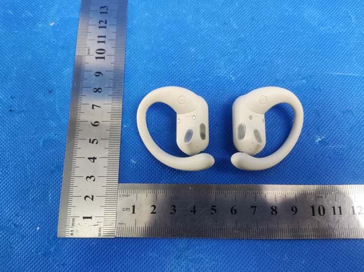
Click to zoom
Application Details
- Equipment Class
- DSS - Part 15 Spread Spectrum Transmitter
- Date of Grant
- Mar 27, 2024
- Application Purpose
- Original Equipment
- Date of Application
- Mar 27, 2024
- Equipment Note
- HEYPLUS OWS
- Frequency Range
- 2402.00000000 - 2480.00000000
- Country
- China
Documents & Files
Document Text
Text extracted from the exhibit documents filed with the FCC. Open a document above to read the original.
Users Manual
A12 Heyplus ows说明书英文: 尺寸75*85mm 展开尺寸:300x85mm 双面印 风琴3折4页 L R HEYPLUS OWS Manual Power On/Off: When the storage box is opened, the earphone automatically turned on, and when the storage box is closed, the earphone turns off. Music mode: Play/Pause: Double-click function key Previous Song: In play status, 3 consecutive clicks on the left ear function key Next Song: In play status, 3 consecutive clicks on the right ear function key Volume -: Press and hold the function button in the left ear to decrease the volume. Volume+: Press and hold the function button on the right ear to increase the volume. Call Mode: Answer/End: Double tap the function key Reject: press and hold the function key for 2 seconds Game/Music Mode: Standby State 3: Click the right ear function key repeatedly Voice Assistant On/Off Standby State 3: Click the left ear function key (the phone must support this function) Functional operation Bluetooth Pairing Connection Bluetooth Pairing: After opening the storage box, the headset automatically enters the Bluetooth pairing mode (red and blue lights flash alternately); the phone searches for " Heyplus ows" and clicks to connect and pair. (If the device is no found, please turn off the Bluetooth of the device and then turn it on again for re-search) Successful Pairing: After successful pairing, the red and blue lights of the headset will turn off, and the headset will emit a prompt tone indicating a successful connection. Automatic Reconnection: After the initial successful connection, the headset will automatically reconnect to the phone in approximately 6 seconds after being turned on. Earphone * 2 Charging compartment * 1 TYPE-C charging cable * 1 Instruction manual * 1 Bluetooth Version: V Model Name: HEYPLUS OWS 5.3 Support Protocol: HSP/HFP/A2DP/AVRCP Frequency Range: 2.40 ~ 2.48 Ghz Horn Specification: 1510 16 ohm Battery Capacity: 70 mAh (earphone) 600 mAH (storage box) Playing Time: about 7 hours (earphone) 30 (storage box) Charging Time: 45 minutes (headset) 2 hours (storage box) Input: 5V/1000mA Output: 5V 300mA Charging Interface: TYPE-C Product Parameters When the left and right earphones cannot be paired or connected to a device, , you can reset them by following these steps: 1. Disconnect and delete the pairing information of "Heyplus ows" from your mobile phone. 2. Put both earphones in the charging compartment . (Make sure that the earphones are not in a low battery state. If they are low on battery,charge them for 5 minutes before performing the reset.) 3. Press and hold the reset button on the charging compartment for 5 seconds to initiate the headset reset. During the reset process, the LED lights on the charging compartment and the earphones will flash three times. 4. After resetting, close the c harging compartment and charge the earphones to complete the reset process. Factory Reset Press and hold for 5 seconds Schematic diagram 1. Do not disassemble, repair or modify the headset for any reason, as it may cause fire, electronic breakdown, or permanent damage to the product. 2. Do not expose the product to excessively low or high humidity environments (below 0 °C or above 45 °C). 3. Do not look directly at the product indicator light when it is turned on, and keep it away from the eyes of children or animals. 4. Do not use this device in thunderstorm weather, as it may cause equipment malfunction or electric shock hazards. 5. Do not use strong chemicals, cleaning agents or harsh detergents to clean equipment or its accessories. 6. Do not put the equipment near heat sources or exposed fire sources, such as electric heaters, microwave ovens, ovens, water heaters, fire candles or other places that may produce high temperatures 7. Do not listen to music at a high volume for a long time to cause hearing damage. Please adjust the appropriate volume when using the equipment. 8. Do not attempt to replace the battery yourself. This device has a non- removable built-in battery, and self-replacement may damage the battery or the device. It is not recommended to replace it privately. 9. Do not contact the magnetic stripe card (such as bank card, telephone card, etc.) with the equipment for a long time, otherwise the magnetic stripe card may be damaged by the magnetic field. 10.Before cleaning and maintenance, stop using the device,close all applications, and disconnect all connections or cables from other devices. Cautions Power On 1. Open the charging compartment cover to turn on the device. 2. Press and hold the MFB key for 2 seconds to start the device. Bluetooth Connection 1. First-time use connection: After opening the storage box, the headset will automatically enter the Bluetooth pairing mode (red and blue lights flashing alternately);Search for "A12" on your phone and click to connect and pair. 2. Successful pairing: After successful pairing, the headset will turn off the r ed and blue lights, and at the same time, the headset will give a prompt tone of successful connection. 3. Automatic reconnection: After the first successful connection, the earphone will be turned on for about 6 seconds in subsequent use. Left and Right Back Connection to the Phone Shut Down 1. When the device is powered on and not connected, touch and hold for 5 seconds to shut it down. Manual shutdown is not supported when it is connected. 2. Put the earphone into the charging compartment, close the cover to shut down the device. Headphones Charging 1. Put the earphone into the charging compartment, close the compartment, and turn off the earphone. 2. Put the earphone into the charging compartment and close the cover for charging. Open Bluetooth Headset Charge for 10 minutes, use for 4 hours Function Description Indicator light Microphone Charging contact Audio output hole Charging thimbleCharging thimble Reset buttonIndicator light Touch function key Product Accessories FCC Statement This device complies with part 15 of the FCC Rules. Operation is subject to the following two condition…
Text truncated - open the document above for the full version.
External Photos
Page 1 of 4 FCC ID: 2AXI9A12 Dongguan Yaxu (AiT) Technology Limited No.22, Jinqianling 3rd Street, Jitigang, Huangjiang, Dongguan, Guangdong, China. External Photos Photo 1 Photo 2 Page 2 of 4 FCC ID: 2AXI9A12 Dongguan Yaxu (AiT) Technology Limited No.22, Jinqianling 3rd Street, Jitigang, Huangjiang, Dongguan, Guangdong, China. Photo 3 Photo 4 Page 3 of 4 FCC ID: 2AXI9A12 Dongguan Yaxu (AiT) Technology Limited No.22, Jinqianling 3rd Street, Jitigang, Huangjiang, Dongguan, Guangdong, China. Photo 5 Photo 6 Page 4 of 4 FCC ID: 2AXI9A12 Dongguan Yaxu (AiT) Technology Limited No.22, Jinqianling 3rd Street, Jitigang, Huangjiang, Dongguan, Guangdong, China. Photo 7 ------End------
ID Label/Location Info
Label FCC ID: 2AXI9A12 Model No:A12
Internal Photos
Page 1 of 3 FCC ID: 2AXI9A12 Dongguan Yaxu (AiT) Technology Limited No.22, Jinqianling 3rd Street, Jitigang, Huangjiang, Dongguan, Guangdong, China. Internal Photos Photo 1 Photo 2 Page 2 of 3 FCC ID: 2AXI9A12 Dongguan Yaxu (AiT) Technology Limited No.22, Jinqianling 3rd Street, Jitigang, Huangjiang, Dongguan, Guangdong, China. Photo 3 Photo 4 Page 3 of 3 FCC ID: 2AXI9A12 Dongguan Yaxu (AiT) Technology Limited No.22, Jinqianling 3rd Street, Jitigang, Huangjiang, Dongguan, Guangdong, China. Photo 5 Photo 6 ------End------ Antenna
RF Exposure Info
RF Exposure evaluation FCC ID: 2AXI9A12 1.1. Applicable Standard According to §1.1307(b)(1), systems operating under the provisions of this section shall be operated in a manner that ensures that the public is not exposed to radio frequency energy level in excess of the Commission’s guidelines. According to §1.1310 and §2.1093 RF exposure requirement KDB447498 v06: Mobile and Portable Devices RF Exposure Procedures and Equipment Authorization Policies 1.2. Requirement According to KDB447498 D01 General RF Exposure Guidance v06 Section 4.3.1 Standalone SAR test exclusion considerations: “Unless specifically required by the published RF exposure KDB procedures, standalone 1-g head or body and 10-g extremity SAR evaluation for general population exposure conditions, by measurement or numerical simulation, is not required when the corresponding SAR Test Exclusion Threshold condition, listed below, is satisfied. These test exclusion conditions are based on source-based time-averaged maximum conducted output power of the RF channel requiring evaluation, adjusted for tune-up tolerance, and the minimum test separation distance required for the exposure conditions.22 The minimum test separation distance is determined by the smallest distance from the antenna and radiating structures or outer surface of the device, according to the host form factor, exposure conditions and platform requirements, to any part of the body or extremity of a user or bystander (see 5) of section 4.1). To qualify for SAR test exclusion, the test separation distances applied must be fully explained and justified by the operating configurations and exposure conditions of the transmitter and applicable host platform requirements, typically in the SAR measurement or SAR analysis report, according to the required published RF exposure KDB procedures. When no other RF exposure testing or reporting is required, a statement of justification and compliance must be included in the equipment approval, in lieu of the SAR report, to qualify for the SAR test exclusion. When required, the device specific conditions described in the other published RF exposure KDB procedures must be satisfied before applying these SAR test exclusion provisions; for example, handheld PTT two-way radios, handsets, laptops & tablets etc.23 “ [(max. power of channel, including tune-up tolerance, mW)/ (min. test separation distance, mm)] · [√f (GHz)] ≤ 3.0 for 1-g SAR and ≤ 7.5 for 10-g extremity SAR, where: • f (GHz) is the RF channel transmit frequency in GHz • Power and distance are rounded to the nearest mW and mm before calculation • The result is rounded to one decimal place for comparison • 3.0 and 7.5 are referred to as the numeric thresholds in the step 2 below The test exclusions are applicable only when the minimum test separation distance is ≤ 50 mm and for transmission frequencies between 100 MHz and 6 GHz. When the minimum test separation distance is < 5 mm, a distance of 5 mm according to 5) in section 4.1 is applied to determine SAR test exclusion. 1.3. Manufacturing tolerance BR - EDR Frequency (MHz) GFSK 2402 2440 2480 Target (dBm) -0.45 -0.59 -1.68 Tolerance ± (dB) 1.0 1.0 1.0 Frequency (MHz) π/4DQPSK 2402 2440 2480 Target (dBm) 0.13 -0.15 -1.19 Tolerance ± (dB) 1.0 1.0 1.0 Page 2 of 2 2. Evaluation Result Evaluation Results Band/Mode f (GHz) Antenna Distance (mm) Max.RF output power (including tune-up tolerance) SAR Test Exclusion Threshold SAR Test Exclusion dBm mW BR-EDR 2.5 5 1.13 1.30 0.41<3 Yes 3. Conclusion The measurement results comply with the FCC Limit per 47 CFR 2.1093 for the uncontrolled RF Exposure and SAR Exclusion Threshold per KDB 447498 v06 .....................End of Report.........................
Test Report
Page1of39ReportNo.:AIT24012514FW1 DongguanYaxu(AiT)TechnologyLimited No.22,Jinqianling3rdStreet,Jitigang, Huangjiang,Dongguan,Guangdong,China. TESTREPORT ClientInformation: Applicant:ShenzhenRB-LINKIntelligentTechnologyCo.,Ltd Applicantadd.: Room401,BuildingC,RunhelndustrialPark,ZhentouRoad,Nandong,Huan gpuCommunity,XinqiaoStreet,BaoanDistrict,Shenzhen,China Manufacturer:ShenzhenRB-LINKIntelligentTechnologyCo.,Ltd Manufactureradd.: Room401,BuildingC,RunhelndustrialPark,ZhentouRoad,Nandong,Huan gpuCommunity,XinqiaoStreet,BaoanDistrict,Shenzhen,China ProductInformation: ProductName:HEYPLUSOWS ModelNo.:A12,Heyplusows,A12Pro,A12Plus,A12+ BrandName:N/A FCCID: 2AXI9A12 Applicablestandards: FCCCFRTitle47Part15SubpartCSection15.247 PreparedBy: DongguanYaxu(AiT)TechnologyLimited No.22,Jinqianling3rdStreet,Jitigang,Huangjiang,Dongguan, Guangdong,China Tel.:+86-769-82020499Fax.:+86-769-82020495 DateofReceipt:Jan.25,2024DateofTest:Jan.25,2024~Jan.26,2024 DateofIssue:Jan.27,2024TestResult:Pass ThisdevicedescribedabovehasbeentestedbyDongguanYaxu(AiT)TechnologyLimitedandthe testresultsshowthattheequipmentundertest(EUT)isincompliancewiththeFCCrequirements. Anditisapplicableonlytothetestedsampleidentifiedinthereport. Note:Thisreportshallnotbereproducedexceptinfull,withoutthewrittenapprovalofDongguan Yaxu(AiT)TechnologyLimited,thisdocumentmaybealteredorrevisedbyDongguanYaxu(AiT) TechnologyLimited,personalonly,andshallbenotedintherevisionofthedocument.Thistest reportmustnotbeusedbytheclienttoclaimproductendorsement. Reviewedby:Approvedby: SimbaHuangSeal.chen Page2of39ReportNo.:AIT24012514FW1 DongguanYaxu(AiT)TechnologyLimited No.22,Jinqianling3rdStreet,Jitigang, Huangjiang,Dongguan,Guangdong,China. 1Contents Page COVERPAGE 1CONTENTS......................................................................................................................................................................2 2TESTSUMMARY............................................................................................................................................................4 2.1StatementoftheMeasurementUncertainty................................................................................4 2.2MeasurementUncertainty............................................................................................................4 3TESTFACILITY..............................................................................................................................................................5 3.1Deviationfromstandard...............................................................................................................5 3.2Abnormalitiesfromstandardconditions.......................................................................................5 3.3TestLocation.................................................................................................................................5 4GENERALINFORMATION...........................................................................................................................................6 4.1Testfrequencies............................................................................................................................7 4.2EUTPeripheralList.......................................................................................................................8 4.3TestPeripheralList.......................................................................................................................8 4.4TESTMETHODOLOGY...............................................................................................................9 4.5DescriptionofTestModes..........................................................................................................10 5EQUIPMENTUSEDDURINGTEST.........................................................................................................................11 6TESTRESULTSANDMEASUREMENTDATA.....................................................................................................11 6.1Antennarequirement..................................................................................................................13 6.2PeakPowerMeasurement.........................................................................................................14 6.3FrequencySeparationand20dBBandwidth............................................................................16 6.4NumberofHoppingFrequency..................................................................................................18 6.5TimeofOccupancy(DwellTime)...............................................................................................19 6.6ConductedSpuriousEmissionsandBandEdgesTest.............................................................21 6.7Restrict-bandBand-edgeMeasurements..................................................................................23 6.8RadiatedEmissionsMeasurement............................................................................................25 6.9ConductedEmissions.................................................................................................................35 6.10Pseudorandomfrequencyhoppingsequence...........................................................................38 7TESTSETUPPHOTOGRAPHSOFEUT.................................................................................................................39 8EXTERNALPHOTOGRAPHSOFEUT....................................................................................................................39 9INTERNALPHOTOGRAPHSOFEUT.....................................................................................................................39 Page3of39ReportNo.:AIT24012514FW1 DongguanYaxu(AiT)TechnologyLimited No.22,Jinqianling3rdStreet,Jitigang, Huangjiang,Dongguan,Guangdong,China. RevisionHistory RevisionIssueDateRevisionsRevisedBy 000 Jan.27,2024 InitialIssueSealChen Page4of39ReportNo.:AIT24012514…
Text truncated - open the document above for the full version.
Test Report
SymbolsLWTA Dimensions 1.60±0.200.80±0.200.80±0.200.30±0.10 NumberTerminalName ① INPUT ② NC ✓Dimensions(Unit: mm) w ①② ( Side View) ( Bottom View) ( Top View) A T L HanyangAntennaDesignCo.Ltd.haspossessionofproprietaryinformationprovidedinthisreportand thisproprietaryinformationshallbekeptinstrictconfidenceandnotdisclosedtoanypersonorfirm withoutthepriorwrittenconsentofHanyangAntennaDesignCo.Ltd. Page1 汉阳天线设计有限公司 HanyangAntenna Design Co. Ltd. 1.Bluetooth 2.Dual-band WLAN 3.ISM and UWB 1.Surfacemountedelementwithasmalldimensionof1.6×0.8×0.8mmmeetfutureminiaturizationtrend. 2.EmbeddedandLTCC(lowtemperatureco-firedceramic)technologyisabletointegratewithsystemdesign aswellasbeatifyingthehousingoffinalproduct. 3.Miniaturization,wideband,highstability,lowESR,andlowtolerance. 4.Dual-bandresonancesinthedominantandharmonicmodesenablesmultibandoperations. 5.Novelground-radiationtechniqueenablesradiationfromboththeantennaandthegroundplane. ▪深圳市宝安区前进二路宝运达物流信息大厦12A10/12A11 ▪青岛市崂山区松岭路399号海信产业园A1号楼606 电话:0755-23069700 传真:0755-23069700 P/N: HY160808 SRF09 ✓Features: ✓Applications: RF chip ANT chipANT pattern PCB ground Mode-2 Mode-1 ✓Layout-1 (3.5mm×6.5mm) HanyangAntennaDesignCo.Ltd.haspossessionofproprietaryinformationprovidedinthisreportand thisproprietaryinformationshallbekeptinstrictconfidenceandnotdisclosedtoanypersonorfirm withoutthepriorwrittenconsentofHanyangAntennaDesignCo.Ltd. Page2 汉阳天线设计有限公司 HanyangAntenna Design Co. Ltd. 1.5 1 3.5 2.5 0201 footprint (E1) 0201 footprint (E2) 0603 footprint (ANT) 连接微带线, 连接RF I/O口 6.5 0.5 0.5 0.5 1.5 3.5 2.5 0201 footprint (E3) 6.5 Top layer: Bottom layer: 0.5 0.5 RF chip E1 E3 E2 ANT ▪深圳市宝安区前进二路宝运达物流信息大厦12A10/12A11 ▪青岛市崂山区松岭路399号海信产业园A1号楼606 电话:0755-23069700 传真:0755-23069700 P/N: HY160808 SRF09 Equivalentcircuit: HanyangAntennaDesignCo.Ltd.haspossessionofproprietaryinformationprovidedinthisreportand thisproprietaryinformationshallbekeptinstrictconfidenceandnotdisclosedtoanypersonorfirm withoutthepriorwrittenconsentofHanyangAntennaDesignCo.Ltd. Page3 汉阳天线设计有限公司 HanyangAntenna Design Co. Ltd. 2.5 0201 footprint 0603 footprint 连接微带线, 连接RF I/O口 10 0.5 1.5 0201 footprint 1.5 3 2.5 10 1.5 2 0.5 0201 footprint ▪深圳市宝安区前进二路宝运达物流信息大厦12A10/12A11 ▪青岛市崂山区松岭路399号海信产业园A1号楼606 电话:0755-23069700 传真:0755-23069700 P/N: HY160808 SRF09 ✓Layout-2 (1.5mm×10mm) Top layer: Bottom layer: HanyangAntennaDesignCo.Ltd.haspossessionofproprietaryinformationprovidedinthisreportand thisproprietaryinformationshallbekeptinstrictconfidenceandnotdisclosedtoanypersonorfirm withoutthepriorwrittenconsentofHanyangAntennaDesignCo.Ltd. Page4 汉阳天线设计有限公司 HanyangAntenna Design Co. Ltd. ▪深圳市宝安区前进二路宝运达物流信息大厦12A10/12A11 ▪青岛市崂山区松岭路399号海信产业园A1号楼606 电话:0755-23069700 传真:0755-23069700 P/N: HY160808 SRF09 5 2 0201 footprint (E1) 0201 footprint (E2) 0603 footprint (ANT) 连接微带线, 连接RF I/O口 7 0.8 5 0201 footprint (E2) 连接微带线, 连接RF I/O口 10 0.8 0603 footprint (ANT) 0201 footprint (E1) ✓Layout-3 (5mm×7mm) ✓Layout-4 (5mm×10mm) 1 3 ✓ElectricalCharacteristics: ✓CharacteristicCurves: FeatureSpecification 1 Centralfrequency2.45GHz&5.5GHz 2 Bandwidth>150MHz 3 Peak gain2~3dBi 4 VSWR<2 5 PolarizationLinear 6 AzimuthbeamwidthOmnidirectional 7 Impedance50Ω HanyangAntennaDesignCo.Ltd.haspossessionofproprietaryinformationprovidedinthisreportand thisproprietaryinformationshallbekeptinstrictconfidenceandnotdisclosedtoanypersonorfirm withoutthepriorwrittenconsentofHanyangAntennaDesignCo.Ltd. Page5 汉阳天线设计有限公司 HanyangAntenna Design Co. Ltd. ▪深圳市宝安区前进二路宝运达物流信息大厦12A10/12A11 ▪青岛市崂山区松岭路399号海信产业园A1号楼606 电话:0755-23069700 传真:0755-23069700 P/N: HY160808 SRF09 ✓RadiationPattern: Y-ZPlane X-ZPlane coordinates: ▪深圳市宝安区前进二路宝运达物流信息大厦12A10/12A11 ▪青岛市崂山区松岭路399号海信产业园A1号楼606 电话:0755-23069700 传真:0755-23069700 HanyangAntennaDesignCo.Ltd.haspossessionofproprietaryinformationprovidedinthisreportand thisproprietaryinformationshallbekeptinstrictconfidenceandnotdisclosedtoanypersonorfirm withoutthepriorwrittenconsentofHanyangAntennaDesignCo.Ltd. Page6 汉阳天线设计有限公司 HanyangAntenna Design Co. Ltd. Frequency 2450MHz5500MHz Avg.gain-0.85-1.30 Peakgain3.03.5 Efficiency82%78% ✓RadiationPerformance: P/N: HY160808 SRF09 Temperature:40±2°C Humidity:90~95%RH Duration:500h Recovery conditions:Room temperature Recovery Time:24h (Class1) or 48h (Class2) Test Temperature Operating Temperature Temperature RelativeHumidity 25°C±5°C -25°C~+125°C 5~40°C 20~70% Notenoughsolder Weak holding forcemay cause bad connection between the chipandPCB. ✓RecommendedSolderingAmounts The optimal solder fillet amounts forre-flowsoldering 天线厚度 以下 The optimal solder fillet amounts for wavesoldering ✓DependabilityTest Too much solder Cracks tend to occur due to large stress. ✓MoistureProof ✓OptimumSolderAmount forReflowSoldering ✓Solderability At least 95% of the terminal electrode is covered by newsolder. Preheating conditions:80 to 120°C;10~30s. Solder Tem p e r at u r e :2 3 5 ±5°C Duration:2 ±0.5s , Solder Tempe r ature:24 5±5°C Du rat ion:2±0.5s HanyangAntennaDesignCo.Ltd.haspossessionofproprietaryinformationprovidedinthisreportand thisproprietaryinformationshallbekeptinstrictconfidenceandnotdisclosedtoanypersonorfirm withoutthepriorwrittenconsentofHanyangAntennaDesignCo.Ltd. Page7 汉阳天线设计有限公司 HanyangAntenna Design Co. Ltd. ▪深圳市宝安区前进二路宝运达物流信息大厦12A10/12A11 ▪青岛市崂山区松岭路399号海信产业园A1号楼606 电话:0755-23069700 传真:0755-23069700 P/N: HY160808 SRF09 10±1S AppliedForce:5NDuration:10±1S Preheating conditions: up-category temperature, 1h Recovery time:24±1h InitialMeasurement Cycling Times: 5 times, 1 cycle, 4steps: Preheating80to120°C;10~30s.SolderTemperature:235±5°C;Duration:2±0.5s;SolderTemperature:245±5°C Duration:2±0.5s;Preheating100to200°C;10±2min. SolderTemperature:265±5°C;Duration:10±1s Cleanthecapacitorwithsolventandexamineitwitha10X(min.)microscope. RecoveryTime:24±2h Recoverycondition:Roomtemperature Test Board: Al 2 O 3 orPCBWarp:1mm Speed:0.5mm/sec. Unit:mm Themeasurementshouldbemadewiththeboardinthe bendingposition. ✓Resistance to Soldering Heat ✓ResistancetoFlexureofSubstrate ✓Temperature CycleTest H…
Text truncated - open the document above for the full version.
Test Report
DongguanYaxu(AiT)TechnologyLimited ReportNo.: AIT24012514FW 1 FCC ID :2AXI9A12 Page1 of42 AppendixA RF Test Data for BT(BDR/EDR)(ConductedMeasurement) ProductName:HEYPLUSOWS TradeMark:N/A Test Model:A12 EnvironmentalConditions Temperature:23.6°C RelativeHumidity:51.3 % ATM Pressure:101Kpa Test Engineer:SimbaHuang Supervisedby:Seal Chen DongguanYaxu(AiT)TechnologyLimited ReportNo.: AIT24012514FW 1 FCC ID :2AXI9A12 Page2 of42 Contents Page COVERPAGE 1Duty Cycle........................................................................................................................................................................................3 1.1Test Result............................................................................................................................................................................3 1.2Test Graphs...........................................................................................................................................................................4 2MaximumConductedPeakOutputPower........................................................................................................................................7 2.1Test Result............................................................................................................................................................................7 2.2Test Graphs...........................................................................................................................................................................8 320dBBandwidth..............................................................................................................................................................................11 3.1Test Result..........................................................................................................................................................................11 3.2Test Graphs.........................................................................................................................................................................12 4CarrierFrequencySeparation.........................................................................................................................................................15 4.1Test Result..........................................................................................................................................................................15 4.2Test Graphs.........................................................................................................................................................................16 5HoppingChannelNumber...............................................................................................................................................................17 5.1Test Result..........................................................................................................................................................................17 5.2Test Graphs.........................................................................................................................................................................18 6DwellTime ......................................................................................................................................................................................19 6.1Test Result..........................................................................................................................................................................19 6.2Test Graphs.........................................................................................................................................................................20 7RF ConductedSpuriousEmissions.................................................................................................................................................22 7.1Test Result..........................................................................................................................................................................22 7.2Test Graphs.........................................................................................................................................................................23 8Band-edgefor RF ConductedEmissions........................................................................................................................................29 8.1Test Result..........................................................................................................................................................................29 8.2Test Graphs.........................................................................................................................................................................30 9Restrict-bandband-edgemeasurements........................................................................................................................................38 9.1Test Result..........................................................................................................................................................................38 9.2Test Graphs.........................................................................................................................................................................39 DongguanYaxu(AiT)TechnologyLimited ReportNo.: AIT24012514FW 1 FCC ID :2AXI9A12 Page3 of42 1 Duty Cycle 1.1Test Result ModeFrequency(MHz)Duty Cycle(%)Correction Factor 1/T (kHz) 1-DH1240232.014.952.56 1-DH1244131.25.062.63 1-DH1248031.25.062.63 2-DH12402324.952.56 2-DH1244132.84.842.5 2-DH12480324.952.56 DongguanYaxu(AiT)TechnologyLimited ReportNo.: AIT24012514FW 1 FCC ID :2AXI9A12 Page4 of42 1.2Test Graphs Test Graphs 1-DH12402MHz 1-DH12441MHz DongguanYaxu(AiT)TechnologyLimited ReportNo.: AIT24012514FW 1 FCC ID :2AXI9A12 Page5 of42 1-D…
Text truncated - open the document above for the full version.
Test Setup Photos
Page 1 of 2 FCC ID: 2AXI9A12 Dongguan Yaxu (AiT) Technology Limited No.22, Jinqianling 3rd Street, Jitigang, Huangjiang, Dongguan, Guangdong, China. Test Setup Photo Radiated Emission Page 2 of 2 FCC ID: 2AXI9A12 Dongguan Yaxu (AiT) Technology Limited No.22, Jinqianling 3rd Street, Jitigang, Huangjiang, Dongguan, Guangdong, China. Conducted Emission ------End------
Contact Information
Applicant
zhiyun Ma(CEO)
Test Firm
Dongguan Yaxu (AiT) Technology LimitedCoin Tang
[email protected]+86 0769-82020499-21
Technical Specifications
| # | Rule Parts | Frequency Range | Power Output |
|---|---|---|---|
| 1 | 15C | 2.40 GHz - 2.48 GHz | 1.00 mW |
Other Applications from Shenzhen RB-LINK Intelligent Technology Co., Ltd
2AXI9-X1
Aug 21, 2026Bone Conduction Camera Headset
Equipment Class
DSS - Part 15 Spread Spectrum Transmitter
2AXI9-C1
Dec 23, 2025Camera Headset
Equipment Class
DSS - Part 15 Spread Spectrum Transmitter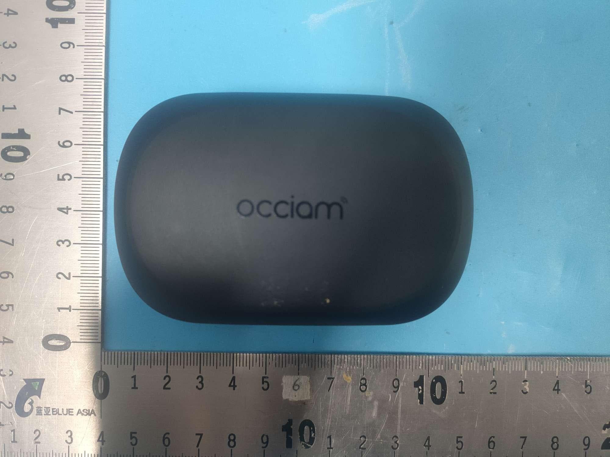
2AXI9T9
Aug 06, 2023True wireless earbuds
Equipment Class
DSS - Part 15 Spread Spectrum Transmitter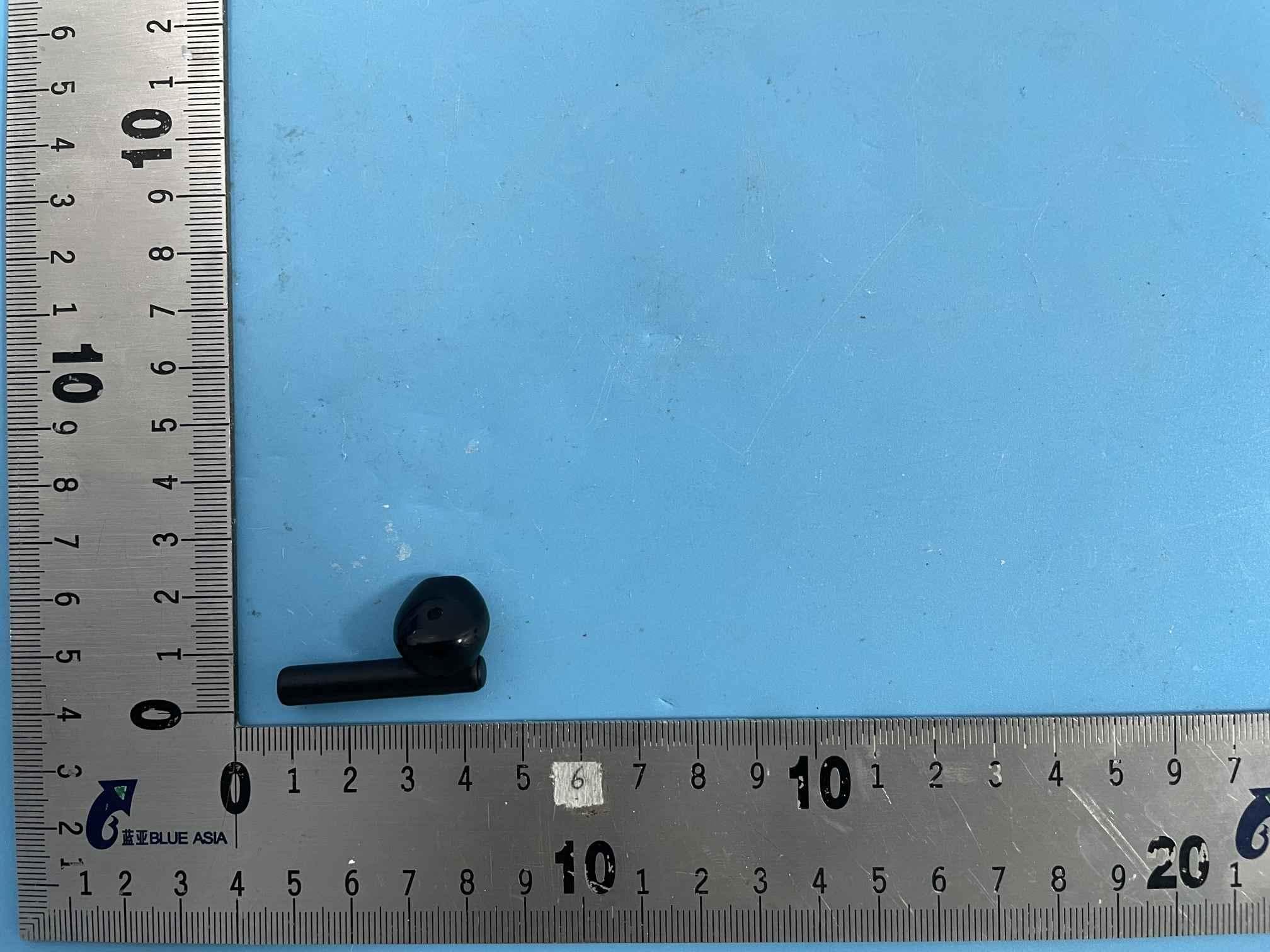
2AXI9S18
Jul 17, 2023True wireless earbuds
Equipment Class
DSS - Part 15 Spread Spectrum Transmitter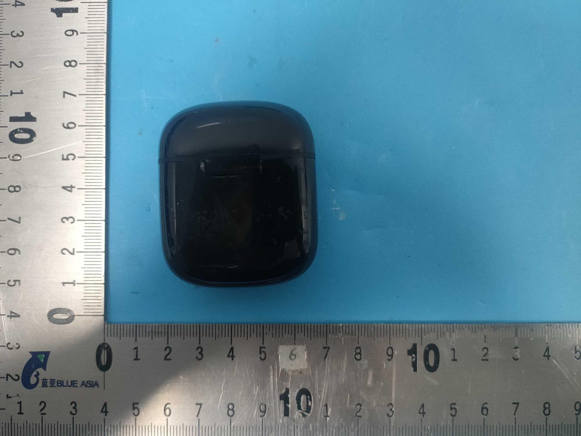
2AXI9IT108
Jul 12, 2023True wireless earbuds
Equipment Class
DSS - Part 15 Spread Spectrum Transmitter