2AYAV-WS-STANDA2010Standing type wireless charger, with fast charging function.
WARP Solution Inc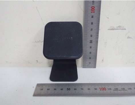
Click to zoom
Application Details
- Equipment Class
- DCD - Part 15 Low Power Transmitter Below 1705 kHz
- Date of Grant
- Feb 07, 2021
- Application Purpose
- Original Equipment
- Date of Application
- Feb 07, 2021
- Equipment Note
- Standing type wireless charger, with fast charging function.
- Frequency Range
- 0.11000000 - 0.20500000
- Company
- WARP Solution Inc
- Country
- South Korea
Documents & Files
Document Text
Text extracted from the exhibit documents filed with the FCC. Open a document above to read the original.
Users Manual
전면 후면 Safety Precautions Please read all the instructions before using the device to ensure safe and proper use. 1. Only charge the product using a charger of appropriate voltage (9V/1.67A recommended). 2. Depending on the location of the charging device on the wireless charging pad, the charging device may not charge properly. 3. Wireless charger may not work properly if you have attached a thick case to your smart device. Please try again after rem oving the case. 4. Do not Press hard or crash or drop the device. 5. Do not disassemble or modify, or repair the device. What’s included? WS-STANDA2010/ USB to C-type Charging Cable/ Instruction Manual/ Non-Slip Sticker Specification 6. Do not put the product near the fire or into the fire, water. 7. Keep wireless charging pad away from any liquids or m oisture, dust, no m etal object between the charging device and the wireless charging pad. 8. Do not expose the product to extreme temperatures or humidity, which may damage the circuits in the product. It is recommended to use your device at room tem peratures. 9. Do not place any magnetic cards or storage media containing magnetic strips on the charging area. Input Output Color Size Weight Product Overview 9V/1.67A (MIN) 10W (MAX) Snow White, Charcoal Black, Peach Beige, Hazy Green 61.5 x 84.3 x 55.2 (mm) 4.23 oz (120g) 10. Do not allow children or anim als to chew or suck the device. 11. Do not use your device for a while if the device is overheated. 12. The device contains magnets. It can affect the operation of implanted pacemakers, cardioverters, defibrillators, insulin pumps or other electro medical devices (collectively, “ Medical Device”) within the range of 15 cm (6 inches). If you are a user of any of these Medical Devices, DO NOT USE THIS DEVICE UNLESS YOU HAVE CONSULTED WITH YOUR PHYSICIAN. 13. Changes or modifications not expressly approved by the party responsible for compliance could void the user’s authority to operate the equipment. 12-Month Limited Warranty A. C-type Input Port B. Charging Pad Surface C. Metal Stand D. Charging Cable A B C D The product has a 12-m onth limited warranty from date of purchase, unless the warranty is voided by one or m ore of the following. To receive service, please have this warranty and receipt with you. After purchasing this product, m ake sure to fill in the information and keep it in a safe place. Exclusion of Warranty Service Charger Instructions 1. Connect the provided charging cable to a compatible AC adaptor or power bank (9V/1.67 recomm ended). Charging Cable 2. Insert the provided charging cable to the C-type input port (A) on the charging pad. 1. In case of loss or damage due to the customer’s fault or negligence (dam age caused by impact or inserting foreign substance) 2. In case of dam age due to personal repair or m odification other than repair provided by the customer center 3. In case of damage due to incorrect use, dropping, liquid damage and im proper use 4. Product damage caused by natural disaster 5. In case of failure after product warranty period Model Name Purchased Location Purchased Date Customer Name This device complies with part 15 of the FCC Rules. Operation is subject to the following two conditions: (1) The device may not cause harmful interference (2) This device must accept any interference received, including interference that may cause undesired operation. FCC ID: 2AYAV-WS-STANDA2010 3. Place your wireless charging enabled device at the center of the wireless charging pad (B). ※ Depending on the surface of your charging device or case, it may slip from the charging surface. Please use the provided non-slip sticker or wipe out the charging pad surface with wet wipes. Copyright © WARP Solution. All Rights Reserved.
Block Diagram
Matching Network Envelope Detector Power Amp DC-DC Converter Power Amp Driver LDO MCU Demodulator Current Sensor SRAM DC-DC Converter LDO H-Bridge Power Inverter Coil Detection Current Sensor MCU PWM Controller Matching Network Tx Coil Tx Coil Wireless Power Transmitter IC for Qi Wireless Power Transmitter IC for Apple watch USB-C Connector Matching Network Envelope Detector Power Amp DC - DC Converter Power Amp Driver LDO MCU Demodulator Current Sensor SRAM DC - DC Converter LDO H - Bridge Power Inverter Coil Detection Current Sensor MCU PWM Controller Matching Network Tx Coil Tx Coil Wireless Power Transmitter IC for Qi Wireless Power Transmitter IC for Apple watch USB - C Connector Power Supply
ID Label/Location Info
먹 1도 먹 1도 먹 1도 백색 1도 Product Name stand:on Model WS-STANDA2010 Color Snow White Input 9V/1.67A(MIN) Output 10W(MAX) KC Certification R-R-WPs-WS-STANDA2010 FCC ID 2AYAV-WS-STANDA2010 Manufacturer WARP Solution Inc. Manufacture Date 2020.12 A/S +81 -70-8835-2555 MADE IN KOREA Product Name stand:on Model WS-STANDA2010 Color Peach Beige Input 9V/1.67A(MIN) Output 10W(MAX) KC Certification R-R-WPs-WS-STANDA2010 FCC ID 2AYAV-WS-STANDA2010 Manufacturer WARP Solution Inc. Manufacture Date 2020.12 A/S +81 -70-8835-2555 MADE IN KOREA Product Name stand:on Model WS-STANDA2010 Color Hazy Green Input 9V/1.67A(MIN) Output 10W(MAX) KC Certification R-R-WPs-WS-STANDA2010 FCC ID 2AYAV-WS-STANDA2010 Manufacturer WARP Solution Inc. Manufacture Date 2020.12 A/S +81 -70-8835-2555 MADE IN KOREA Product Name stand:on Model WS-STANDA2010 Color Charcoal Black Input 9V/1.67A(MIN) Output 10W(MAX) KC Certification R-R-WPs-WS-STANDA2010 FCC ID 2AYAV-WS-STANDA2010 Manufacturer WARP Solution Inc. Manufacture Date 2020.12 A/S +81 -70-8835-2555 MADE IN KOREA
Operational Description
Stand:ON Model Number: WS – STANDA2010 Manufacture: WARP Solution Inc. Country of origin: KOREA Operating Frequency: 128.1 KHz Antenna Type: Loop Coil Antenna Modulation Type: ASK Channel Spacing: 1 Input: 9V/1.67A (MIN) Output: 10W (MAX) 10w Wireless bate Product Description 10w wireless charger bate wireless charging transmitting module, It is a transmitter specially designed to meet the wireless receiving requirements of QI standard; Module complies with WPC1.1. Using chip CWT-100 of Jiangxi Lianzhi integrated circuit Co., Ltd, Stable performance, Low standby power consumption; Adopt unique PWM modulation mode, Greatly improve conversion efficiency, Easily realize the convenience brought by wireless; High module output efficiency, The comparison between the built-in transmission power and the wireless reception power, More accurate control of the loss of emission energy. The number of module components is small, and the cost performance is high. No debugging is needed, just install and use. I can easily meet the requirements of certification and is very suitable for all kinds of wireless charging equipment complying with Qi standard. For example: for mobile devices with wireless charging function. Product characteristics 1. It is designed in strict accordance with Qi standard and is compatible with all kinds of Reception conforming to Qi standard 2. Current induction 3. The modules has over-current protection (OCP) 4. Over current limit; Short circuit protection; 5. Under voltage protection(UVP); Over voltage protection(OVP); Foreign metal detection(FOD), etc; 6. Over temperature protection (OTP) 7. The standby power consumption is less than 0.09w, the efficiency is about 76% Product job description 1. Place Qi wireless receiving product above the center of coil of the product(transmitting Module). At this time, Qi wireless receiving product shall output voltage and current, and the Red and blue lights shall be on for 3 seconds at the same time and then go out 2. If the Qi wireless receiving equipment is far away from the coil center of the transmitting module, it cannot enter the charging state. At this time, the Qi wireless receiving device needs to be moved back to the central position of the coil of the transmitting module, so that it can automatically enter the charging state. Red and blue lights away on at the same time. 3. If the transmitting module detects that the Qi wireless receiver is abnormal, the red and blue lights flash twice, and the transmitting module does not work. At this time, it is necessary to remove the receiving device from the transmitting module, and put the receiving device on the transmitting module again to enter the charging state.
RF Exposure Info
FCC ID : 2AYAV-WS-STANDA2010 Measuring Standard Tested by Reviewed by Test Items Maximum Permissible Exposure Abbreviation (Signature) None Result (Pass / Fail)Remark Page 1 of 4 Report No. : ESTRFC2102-001 Product name : STAND:ON Model name : WS-STANDA2010 Date of Test : 2021, 02, 02 Engineer H.G. Lee(Signature) Engineering Manager I.K. Hong Declaration of Conformity: The test results with all measurement uncertainty excluded are presented in accordance with regulation limits or requirements declared by manufacturers. Comments and Explanations: Pass- RF Exposure Evaluation Description of EUT KDB 680106 D01 RF Exposure Wireless Charging Apps v03 Pass = Complied, Fail = Failed, N/A = not applicable ModelCal. Due Date ELT-40024-Dec-21 Requirements According to the item 5 of KDB 680106 D03v01: Induction wireless power transfer applications that meet all of the following requirements of KDB 680106 D01, Clause 5(b) is waived from PAG procedures. (1) Power transfer frequency is less than 1 MHz. (conform) (2) Output power from each primary coil is less than or equal to 15 watts. (conform) (3) The transfer system includes only single primary and secondary coils. This includes charging systems that may have multiple primary coils and clients that are able to detect and allow coupling only between individual pairs of coils. (conform) (4) Client device is placed directly in contact with the transmitter. (conform) (5) Mobile exposure conditions only (portable exposure conditions are not covered by this exclusion). (conform) (6) The aggregate H-field strengths at 15 cm surrounding the device and 20 cm above the top surface from all simultaneous transmitting coils are demonstrated to be less than 50% of the MPE limit. (conform) Page 2 of 4 Test equipment List DescriptionManufacturer Magnetic fileld meterNARDA 1 Human Exposure Assessment 1.1.1 Limit of Maximum Permissible Exposure Magnetic Field Strength(A/m) Power Density (mW/cm 2 ) Average Time (minutes) 1.63 * (100) 6 4.89/f * (900/f 2 ) 6 0.1631.06 F/3006 56 Magnetic Field Strength(A/m) Power Density (mW/cm 2 ) Average Time (minutes) 1.63 * (100) 30 2.19/f * (180/f 2 ) 30 0.0730.230 -F/150030 -1.030 F = Frequency in MHz * = Plane-wave equivalent power density Test setup Page 3 of 4 0.3 - 3.0614 3.0 - 301842/f 1.1 Maximum Permissible Exposure Limits for Occupational / Controlled Exposure Frequency Range (MHz) Electric Field Strength (V/m) 30 - 30061.4 300 - 1500 1500 - 100,000 Limits for General Population / Uncontrolled Exposure Frequency Range (MHz) Electric Field Strength (V/m) 300 - 1500- 1500 - 100,000- 0.3 - 1.34614 1.34 - 30824/f 30 - 30027.5 Test Procedure 1) The RF exposure test was performed in anechoic chamber. 2) The measurement probe was placed at test distance (15 cm from all sides and 20 cm from the top) which is between the edge of the charger and the geometric center of probe. 3 ) The highest emission level was recorded and compared with limit as soon as measurement of each points (A, B, C, D, E) were completed. 4) The EUT was measured according to the dictates of KDB 680106 D03v01. Test Result Test Set-up Photo ----0.0541.63 H-Filed Strength at 20 cm from the Top Test Position A Test Position B Test Position C Test Position D Test Position E Limits Test (A/m) Test Position C Test Position D Test Position E Limits Test (V/m) ----2.48614 0.0790.0810.0740.072-1.63 E-Filed Strength at 15 cm from the edges surrounding the EUT H-Filed Strength at 15 cm from the edges surrounding the EUT Test Position A Test Position B Test Position C Test Position D Test Position E Limits Test (A/m) E-Filed Strength at 20 cm from the Top Test Position A 2.42.522.342.45-614 Page 4 of 4 Test Position A Test Position B Test Position C Test Position D Test Position E Limits Test (V/m) Test Position B
Schematics
1 1 2 2 3 3 4 4 5 5 6 6 DD CC BB AA Title NumberRevisionSize A4 Date:2019/10/19Sheet of File:E:\2019工作文件\..\TL15A3870-10-15WLZ.SchDocDrawn By: Qi qual i f i cat i on pat h Rever si on No. : Title 1.4.1 Cel f r as Chi p Devel opment Scal e Code Descr i pt i on: SHEET: OF #NAME? ** REV:SI ZE:CODE: DRAWN:DATED: DATED:CHECKED: QUALI TY CONTROL:DATED: DATED:RELEASED: COMPANY: TI TLE: DRAWI NG NO: SCALE: REVI SI ON RECORD A B C D DATE: 123456 D C B A APPROVED: VPP 1 LDO33 2 LDO18 3 GND_DCDC 4 DCDC_SW 5 VIN 6 LDO_IN 7 LDO50 8 ENB 9 GND_REF 10 L E D 1 1 1 L E D 2 1 2 V D D _ I O 1 3 G P I O 0 _ S C L 1 4 G P I O 1 _ S D A 1 5 G P I O 2 1 6 G P I O 3 1 7 G P I O 4 1 8 G P I O 5 1 9 G P I O 6 2 0 GPIO7 21 PA_GH2 22 PA_BST2 23 PA_SW2 24 PA_GL2 25 GND_DRV 26 PA_GL1 27 PA_SW1 28 PA_BST1 29 PA_GH1 30 V D D _ D R V 3 1 P A _ B R G 3 2 A N A _ T E S T 3 3 E X T _ T S 3 4 D M O D _ V I N 3 5 C O I L _ V I N 3 6 I S _ O U T 3 7 G N D _ S N S 3 8 I S _ I N N 3 9 I S _ I N P 4 0 E P 4 1 U1 CWQ1000 1 0 0 n F / 1 0 V C 2 1 u F / 1 0 V C 1 1 0 0 n F / 1 0 V C 4 N C / 1 u F / 1 0 V C 3 N C / 1 0 u F / 1 0 V C 6 1 0 0 n F / 1 0 V C 7 1uF/10V C10 100K/5% R1 1 1 2 2 LED/ SMD/ 0603Gr een D1 1 1 2 2 LED/ SMD/ 0603Red D2 1K/5% R2 1K/5% R3 1uF/10V C11 N C / 5 6 p F / 1 6 V C 1 2 27R/1% R5 27R/1% R6 100nF/16V C15 100nF/16V C16 27R/1% R9 27R/1% R10 1 0 0 K / 1 % R 1 1 1 0 0 K / 1 % R 1 2 1 0 0 K / 1 % R 1 3 1 0 0 K / 1 % R 1 4 2 2 n F / 2 5 V C 1 7 0 . 1 R / 1 % R 1 5 10 0nF/16V C19 10uF/16 V C20 2 2 n F / 2 5 V C 2 1 0 . 1 R / 1 % R 1 6 1 1 TP4 NC/100V/NP 0 C22 NC/100V/NP 0 C23 NC/10 0V/NP0 C24 10 0nF/16V C28 10 uF/16V C29 1 0 u F / 1 0 V C 0 6 0 3 C 3 0 1 0 0 n F / 1 0 V / N C C 3 1 100nF/16 V C32 1 0 R / 5 % R 1 7 1 0 R / 5 % R 1 8 1 0uF/16V C06 03 C33 0.02R/1% R0805 R19 2 2 u F / 1 6 V C 1 2 0 6 C 3 5 1 1 TP3 6 8 0 p F / 1 6 V C 3 6 22nF/ 50V C37 1K/1% R2 0 5 . 6 n F / 5 0 V / X 7 R C 3 8 2 0 0 K / 1 % R0603 R 2 1 2.4K/1% R22 10K NTC/ SMD/ WI RE R24 1 8 K / 1 % R 2 5 1K/1% R26 BAV21W D3 CS# 1 DO 2 WP# 3 GND 4 DIO 5 CLK 6 HOLD# 7 VCC 8 U2 FLASH/SOP8/ZD25D 100nF/10V C39 M P - A 2 L 2 T X _ C O I L 1 0 0 n F / 1 6 V C 4 1 1 0 u F / 1 6 V C 4 3 1 1 TP7 1 1 T P 6 N C / 4 . 7 K / 5 % R 7 N C / 4 . 7 K / 5 % R 8 5.6nF/50V/X7R C0603 C45 BAV21W D4 33 0K/1 % R4 1 1 0 0 K / 1 % R 4 2 2K/5 % R4 3 3 9 0 K / 5 % R 4 4 1 0 0 K / 5 % R 4 5 5 . 6 n F / 5 0 V / X 7 R C 4 6 1 n F / 2 5 V C 4 7 1 1 TP1 J2A J2B J2C J2D NC/10 0V/NP0 C25 CBB21-254 J1 00V C13 K A S MF1 3A(OG) D5 18KR51 4 . 7 K / 5 % R 4 7 1K/5% R52 1 2 7 8 6 5 4 3 Q 1 1 2 7 8 6 5 4 3 Q 2 LDO33 LDO33 LDO33 LDO33 LDO33 LDO33 LDO33 LDO33 LDO33 LDO18 GPI O2_SCK GPI O2_SCK GPI O3_CSN GPI O3_CSN VCC_5V VCC_5V GPI O4_MOSI GPI O4_MOSI GPI O5_MI SO GPI O5_MI SO VI N VI N VI N COI L_VI N COI L_VI N A N A _ T E S T I S_I NP I S_I NP I S_I NN I S_I NN LDO50 G P I O 6 GPIO6 GND GPIO7 GPIO7 LED1 L E D 2 SCL SCL PA_GH1 PA_GH2 PA_BST1 PA_BST2 PA_GL1 PA_GL2 V_BRI DGE V_BRI DGE V_BRI DGE I S _ O U T SDA SDA DMOD_VIN ENB ENB GNDGND LDO33 GNDGND GND GND VCC_5V GNDGND VIN LDO33 LDO33 GND G P I O 2 _ S C K G P I O 3 _ C S N G P I O 4 _ M O S I G P I O 5 _ M I S O GND I S _ I N P I S _ I N N GND GND GND GND GND V_BRIDGE GND GND V_BRIDGE GNDGND GND V_BRIDGE GND VIN IS_INPIS_INN GND L D O 3 3 GND GPIO3_CSN GND GPIO2_SCK GPIO4_MOSI GND GND VIN GND GPIO5_MISO VCC_5V L D O 3 3 LDO33 LDO33 LDO33 GND GND GND COIL_VIN G P I O 6 C O I L _ V I N GNDGNDGND GND ENB SCL SDA GND E N B S C L S D A GPIO7 GPIO6 L D O 3 3 GPIO7 GND GND 2 2 u F / 2 5 V C 5 12 34 56 78 J8 4X2 排针 VIN D- D+ GND
Test Report
Test Report for FCC Company name Address Telephone Product name Model No. Serial No. Test date Testing location Standard □ Class A ■ Class B Test resultOK □ Class A ■ Class B Test resultOK Tested by Reviewed by Abbreviation * Note - This test report is not permitted to copy partly without our permission - This test result is dependent on only equipment to be used - This test result based on a single evaluation of one sample of the above mentioned Report Number : ESTRFC2012-006 EST-QP17-R-IO1-F04 (2019.11.01) Page 1 of 17 Date of issue 347-69, Jungbu-daero 147beon-gil, Majang-myeon, Icheon-si, Gyeonggi-do 467-811, R. O. Korea Test item FCC PART 15 Subpart C(15.209), ANSI C 63.10(2013) OK, Pass = Complied, Fail = Failed, N/A = not applicable Measurement facility registration number Engineer H.G. Lee(Signature) ■ Radiated Emission Engineering Manager I.K. Hong(Signature) KOREA 28-Dec-2014-Dec-20 ~ 15-Dec-20 ■ Conducted Emission 659627 Product Country of origin STAND:ON WS-STANDA2010 NONE WARP Solution Inc.Manufacturer WARP Solution Inc. Applicant 307, (Guseong-dong), 291, Daehak-ro, Yuseong-gu, Daejeon, Republic of Korea +82-02-532-2555 Report NumberESTRFC2012-006 FCC ID : 2AYAV-WS-STANDA2010 3 4 5 6 8 8 8 8 9 10 10 10 10 11 7. Measurement of conducted emission ............................................................ ...13 7.1 Measurement equipment ........................................................................... 13 7.2 Environmental conditions ........................................................................... 13 7.3 Test data ................................................................................................ 14 8. Photographs of test setup .............................................................................. 15 9. Photographs of EUT .................................................................................... ...17 6.1 Radiated emission limits, general requirements .......................................... ... 5.4 Test data ................................................................................................ 6.3 Environmental conditions ........................................................................ ... 6.4 Test data ................................................................................................ 6.2 Measurement equipment ........................................................................... 6. Measurement of radiated emission .................................................................. Report Number : ESTRFC2012-006 EST-QP17-R-IO1-F04 (2019.11.01) Page 2 of 17 Appendix 1. Special diagram Appendix 2. Antenna Requirement Contents 1. Laboratory Information .................................................................................... 2. Description of EUT .......................................................................................... 3. Test Standards ............................................................................................. 5.3 Environmental conditions ........................................................................ ... 4. Measurement condition ................................................................................. 5. 20 dB Bandwidth............................................................................................. 5.1 Radiated emission limits, general requirements .......................................... ... 5.2 Measurement equipment ........................................................................... 1. Laboratory Information 1.1 General 1.2 Test Lab. Corporation Name : ESTECH Co., Ltd. 1.3 Official Qualification(s) KCC : Granted Accreditation from Ministry of Information & Communication for EMC, Safety and Telecommunication KOLAS : Accredited Lab By Korea Laboratory Accreditation Schema base on CENELEC FCC : Filed Laboratory at Federal Communications Commission VCCI : Granted Accreditation from Voluntary Control Council for Interference from ITE This EUT (Equipment Under Test) has been shown to be capable of compliance with the applicable technical standards and is tested in accordance with the measurement procedures as indicated in this report.ESTECH Lab attests to accuracy of test data. All measurement reported herein were performed by ESTECH Co., Ltd. ESTECH Lab assume full responsibility for the completeness of these measurements and vouch for the qualifications of all persons taking them. Report Number : ESTRFC2012-006 EST-QP17-R-IO1-F04 (2019.11.01) Page 3 of 17 Head Office : Suite 1015 World Meridian II, 123 Gasan Digital 2-ro, Geumcheon-gu, Seoul 153-759, R. O. Korea EMC/Telecom/Safety Test Lab : 347-69, Jungbu-daero 147beon-gil, Majang-myeon, Icheon-si, Gyeonggi-do 467-811, R. O. Korea 2. Description of EUT 2.1 Summary of Equipment Under Test Product: Model Number: WS-STANDA2010 Serial Number: Manufacturer: Country of origin : Operating Frequency : 128.1 kHz Antenna Type: Loop Coil Antenna Modulation Type: ASK Channel Spacing : 1 Power Rating : Receipt Date: X-tal list(s) or Frequencies generated : 2.2 General descriptions of EUT Ripple Voltage<120 mV Lighting mode The Charging indicator flashes red and blue altemately for 3 times before going out, working status:blue light breathing. FOD status: red light flashing, full light not on PCBA module sizelong: 44 mm wide: 30 mm thick: 3.5 mm Compatibility Compatible with Qi receiving products on the market, Samsung mobile / Apple Mobile / Huawei mobile; Input voltage Transmitting Frequency Charging Distance Coil type Diameter:50 mm * thick:2.0 mmSize of magnetic disc plus coil 75% 110 KHz ~ 205 KHz 2 mm - 8 mm Model: A11, Inductance Value: 6.3 uH Report Number : ESTRFC2012-006 EST-QP17-R-IO1-F04 (2019.11.01) Page 4 of 17 The highest operating frequency is 128.1 kHz STAND:ON NONE WARP Solution Inc. KOREA Input:100-240 V AC 50/60 Hz Output: DC 9 V 1.1A 20-Oct-20 9V/1.1A Conversion effciency 3. Test Standards Test Standard : FCC PART 15 Test Method : ANSI C 63.10 (20…
Text truncated - open the document above for the full version.
Contact Information
Applicant
Lee Kyunghak
Test Firm
ESTECH Co., Ltd.Yang Jinmo
Technical Specifications
| # | Rule Parts | Frequency Range | Power Output |
|---|---|---|---|
| 1 | 15C | 0.11 MHz - 0.205 MHz | - |