2AYT2-VG63S9SC2AWireless Module
Shenzhen Vollgo Technology co., Ltd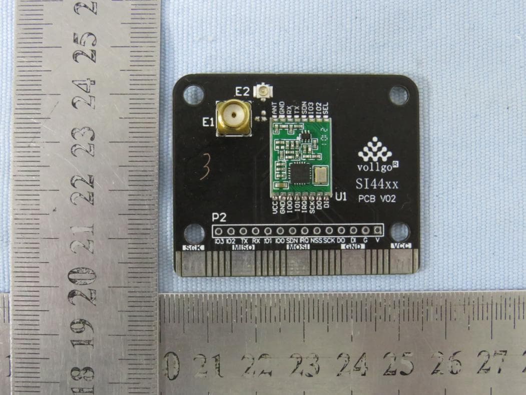
Click to zoom
Application Details
- Equipment Class
- DXX - Part 15 Low Power Communication Device Transmitter
- Date of Grant
- Mar 01, 2021
- Application Purpose
- Original Equipment
- Date of Application
- Mar 01, 2021
- Equipment Note
- Wireless Module
- Frequency Range
- 915.00000000 - 916.00000000
- Country
- China
Documents & Files
Document Text
Text extracted from the exhibit documents filed with the FCC. Open a document above to read the original.
Users Manual
SI4463S9S-V1-C2A SUB-1G Wireless Module SI4463S9S-V1-C2A Wireless Module Hardware Specifications V01 Company: Shenzhen Vollgo Technology co., Ltd Address: No.1 Sanhe Road, Gaofeng Community Dalang Street, Longhua District, Shenzhen, Guangdong, 518104 China Contact: 0755-23040053 SI4463S9S-V1-C2A SUB-1G Wireless Module directory 1. Overview ...................................................................................................................................... 1 2. Technical parameters .................................................................................................................... 2 3. Pin Assignments ........................................................................................................................... 3 4. Pin Description ............................................................................................................................. 4 5. Recommended Connection of Hardware ...................................................................................... 5 6. Revision History ........................................................................................................................... 6 7. Document Statement .................................................................................................................... 6 8. FCC and IC Statements ................................................................................................................ 6 FCC Statements ........................................................................................................................ 6 IC Statement ............................................................................................................................. 8 General Statements ................................................................................................................. 10 SI4463S9S-V1-C2A SUB-1G Wireless Module 1 www.vollgo.com 1. Overview Si4463SXS series wireless module, based on Silicon Labs Si4463 C version of high- performance wireless transceiver chip design, is a small size, low power consumption, long- distance two-way wireless transceiver module. SI4463 is one of the ISM band wireless transceiver chips launched by Silicon Labs, with industry-advanced RF performance.The module integrates all RF related functions and devices. Users can easily develop stable and reliable wireless solutions and wireless Internet of Things devices using this module without in-depth understanding of RF circuit design. Applications : 1) Logistics tracking, warehouse inspection, intelligent home appliances, electronic tags, etc 2) Replace 232, 485 for wireless data communication 3) Wireless data acquisition and control for industrial instruments and meters 4) AMR (water, electricity and gas) meter reading 5) Building and residential (smart home) controls 6) Wireless remote control for consumer electronics 7) Wireless alarm and security system 8) Wireless sensor network SI4463S9S-V1-C2A SUB-1G Wireless Module 2 www.vollgo.com 2. Technical parameters Characteristics Parameter Note Chip Si4463-C2A-GMR Supply Voltage Range 1.8 V to 3.8 V Generally 3.3 V Operation Frequency Range 915 MHZ to 916 MHZ Programmable Modulation Type 2FSK RX Sensitivity 915Mhz -110dBm @10Kbps /2FSK Output Power 10dBm(10mW) Maximum RX Mode Current 14mA TX Mode Current <100mA Sleep Mode Current <1uA Data Rate 10Kbps Deviation 20KHz Channel Number 5 Channel Separation 250KHz Antenna Impedance 50 ohm Driver interface Serial Peripheral Interface Operating Temperature Range - 40 °C ~ 85 °C Storage Temperature Range -55 °C ~ 150 °C Packing Type Blister tray or reel Module Size 16.0 mm x 12.0 mm x 1.8 mm Width tolerance: +/-0.5mm SI4463S9S-V1-C2A SUB-1G Wireless Module 3 www.vollgo.com 3. Pin Assignments SI4463S9S-V1-C2A SUB-1G Wireless Module 4 www.vollgo.com 4. Pin Description Pin Pin Name I/O Description 1 VCC - +1.8 to +3.8V Supply Voltage Input to Module The recommended VCC supply voltage is +3.3V 2 GND - The ground of the power supply 3 IO0 I/O Direct connection chip GPIO0 digital I/O pin, software Settings 4 IO1 I/O Direct connection chip GPIO1 digital I/O pin, software Settings 5 IRQ O NIRQ interrupts the output pin and outputs low level when an interrupt is generated 6 SCK I SPI interface SCLK clock input 7 SDO O SPI interface MISO data output 8 SDI I SPI interface MOSI data input 9 SEL I SPI interface NSEL select input 10 IO2 I/O Direct connection chip GPIO2 digital I/O pin, software Settings 11 IO3 I/O Direct connection chip GPIO3 digital I/O pin, software Settings 12 SDN I Shutdown Input Pin ,SDN=0 for all modes except shutdown mode,When SDN=1 the module will be completely shut down and the contents of the internal registers Will be lost 13 TX I RF swtich TX path control port When In TX mode Tx =1;RX=0 14 RX I RF switch RX path control port When In RX Mode Tx =0; RX=1 15 GND - The ground of the power supply 16 RF I/O The RF signal input/output Port ,50 Ω SI4463S9S-V1-C2A SUB-1G Wireless Module 5 www.vollgo.com 5. Recommended Connection of Hardware Figure 5-1 Hardware Connection Antenna Path design: The following figure gives an overview of a design with Ipex connector for antenna and soldering for Integral Antenna. Figure 5-2: RF module Test Board The antenna path must be designed with a 50 OHMS line inserted into The ground plane for better performance. Antenna must be kept away from any metal part like batteries, etc... for better performance. SI4463S9S-V1-C2A SUB-1G Wireless Module 6 www.vollgo.com 6. Revision History Revision Comment Ddate Author V01 First release October 4, 2019 7. Document Statement 1. Due to product version upgrade or other reasons, this document will be updated from time to time.Unless otherwise agreed, this document is intended as a guide to use only, and all statements, information and recommendations contained in this document do not constitute any warranty, express or implied. 2. The Company reserves the right of final i…
Text truncated - open the document above for the full version.
Cover Letter(s)
C5266091_X10_Ed.1 1/1 Shenzhen Vollgo Technology co., Ltd Office of Engineering Technology Federal Communications Commission 7435 Oakland Mills Road Columbia, MD 21046 Date: 2/23/2021 Subject: Request for Confidentiality FCC ID: 2AYT2-VG63S9SC2A To Whom It May Concern, Pursuant to the provisions of Sections 0.457 and 0.459 of Commission's rules (47CFR0.457, 0.459), we are requesting the Commission to withhold the following attachment(s) as confidential document from public disclosure. Exhibits Long-Term Confidentiality Short-Term Confidentiality ID Label/Location No No Attestation Statement No No External Photos No Block Diagram Schematics Test Report No No Test Setup Photos No User’s Manual Internal Photos Parts List / Tune Up RF Exposure Info Operational Description Cover Letter(s) No No SDR Software / Security Info No Above mentioned document contains detailed system and equipment description are considered as proprietary information in operation of the equipment. The public disclosure of above documents might be harmful to our company and would give competitor an unfair advantage in the market. It is our understanding that all measurement test reports, FCC ID label format and correspondent during certification review process cannot be granted as confidential documents and those information will be available for public review once the grant of equipment authorization is issued. Sincerely, Signature: Name: Jun Liao Title: Manager
External Photos
FCC ID: 2AYT2-VG63S9SC2A IC: 26935-VG63S9SC2A External and Internal photos Test Fixture with control tool Test Fixture with mother board FCC ID: 2AYT2-VG63S9SC2A IC: 26935-VG63S9SC2A RF chipset FCC ID: 2AYT2-VG63S9SC2A IC: 26935-VG63S9SC2A Antenna - RF915-1 Antenna - RF915-1 FCC ID: 2AYT2-VG63S9SC2A IC: 26935-VG63S9SC2A Antenna - RF915-2 Antenna - RF915-2
ID Label/Location Info
Label Label Location Wireless Module Model: SI4463S9S-V1-C2A Input: 3.3V 100mA FCC ID: 2AYT2-VG63S9SC2A IC: 26935-VG63S9SV2A Vollgo
Internal Photos
FCC ID: 2AYT2-VG63S9SC2A IC: 26935-VG63S9SC2A External and Internal photos Test Fixture with control tool Test Fixture with mother board FCC ID: 2AYT2-VG63S9SC2A IC: 26935-VG63S9SC2A RF chipset FCC ID: 2AYT2-VG63S9SC2A IC: 26935-VG63S9SC2A Antenna - RF915-1 Antenna - RF915-1 FCC ID: 2AYT2-VG63S9SC2A IC: 26935-VG63S9SC2A Antenna - RF915-2 Antenna - RF915-2
Test Report
Report No.: NTC2101270FV00 Page 2 of 49 Table of Contents 1. Summary of Test Result ...................................................................................................................................... 4 2. General Description of EUT ................................................................................................................................ 5 3. Test Channels and Modes Detail ........................................................................................................................ 7 4. Configuration of EUT ........................................................................................................................................... 7 5. Modification of EUT ............................................................................................................................................. 7 6. Description of Support Device ............................................................................................................................. 8 7. Test Facility and Location ................................................................................................................................... 9 8. Applicable Standards and References ................................................................................................................ 9 9. Deviations and Abnormalities from Standard Conditions ................................................................................. 10 10. Test Conditions ............................................................................................................................................... 10 11. Measurement Uncertainty ............................................................................................................................... 10 12. Sample Calculations ....................................................................................................................................... 11 13. Test Items and Results ................................................................................................................................... 12 13.1 Conducted Emissions Measurement ............................................................................................................ 12 13.2 Radiated Spurious Emissions and Fundamental Emissions Measurement ................................................. 18 13.3 20dB Bandwidth Measurement ..................................................................................................................... 46 13.4 Antenna Requirement ................................................................................................................................... 48 14. Test Equipment List......................................................................................................................................... 49 Report No.: NTC2101270FV00 Page 3 of 49 Revision History Report Number Description Issued Date NTC2101270FV00 Initial Issue 2021-02-24 Report No.: NTC2101270FV00 Page 4 of 49 1. Summary of Test Result FCC Rules Description of Test Result Remarks §15.207 (a) AC Power Conducted Emission PASS --- §15.249(a) Field Strength Fundamental Emissions PASS --- §15.249(a),(d) 15.209, 15.205 Radiated Spurious Emissions PASS --- §15.215(c) 20dB Bandwidth PASS --- §15.203 Antenna Requirement PASS --- Report No.: NTC2101270FV00 Page 5 of 49 2. General Description of EUT Product Information Product Name: Wireless Module Main Model Name: SI4463S9S-V1-V2A Additional Model Name: N/A Model Difference: N/A S/N: 20201000001 Brand Name: Vollgo Hardware Version: V01 Software Version: V01 Rating: DC 3.3V Typical arrangement: Table-top I/O Port: N/A Accessories Information Adapter: N/A Cable: N/A Other: N/A Additional Information Note: N/A Remark: All the information above are provided by the manufacturer. More detailed feature of the EUT please refers to the user manual. Report No.: NTC2101270FV00 Page 6 of 49 Technical Specification Frequency Range: 915-916MHz Modulation Type: 2FSK Number of Channel: 5 (refer to following channel list for details) Channel Space: 250KHz Antenna Type: External antenna (refer to following antenna information for details) Antenna Gain: 1.0 dBi and 2.0 dBi (refer to following antenna information for details) Channel List Channel Frequency (MHz) Channel Frequency (MHz) Channel Frequency (MHz) 0 915.00 --- --- --- --- 1 915.25 --- --- --- --- 2 915.50 --- --- --- --- 3 915.75 --- --- --- --- 4 916.00 --- --- --- --- Antenna Information Antenna Manufacturer M/N Antenna type Connection type Gain 1 Shuodian RF915-1 FPC Soldering 1 2 Shuodian RF915-2 FPC Ipex-1 2 Note: Since the connection type of the two antennas is different, both of the antennas are considered and tested. Report No.: NTC2101270FV00 Page 7 of 49 3. Test Channels and Modes Detail Mode Channel Frequency (MHz) Modulation Data Rate (Kbps) 1 TX Low 0 915.00 2FSK 10 Mid 2 915.50 2FSK 10 High 4 916.00 2FSK 10 Note: TX mode means that the EUT was programmed to be in continuously transmitting mode. 4. Configuration of EUT TX Mode 5. Modification of EUT No modifications are made to the EUT during all test items. EUT Laptop Adapter Test Fixture Report No.: NTC2101270FV00 Page 8 of 49 6. Description of Support Device The EUT has been tested as an independent unit together with other necessary accessories or support units. The following support units or accessories were used to form a representative test configuration during the tests. No. Equipment Brand M/N S/N Cable Specification Remarks 1. Laptop HUAWEI HBL-W19 M3VPM19C 05000965 Power cord, 1.15m, shielded --- 2. Power supply (Laptop) HUAWEI HW-200325 CP0 N/A --- 3. Test Fixture Vollgo --- --- USB Cable, 1.2m, shielded, with a ferrite core Provided by the manufacturer No. Test Software Modulation Power Setting 1. No test software was used. The test fixture used for testing. 2FSK 0x0b Report No.: NTC2101270FV00 Page 9 of 49 7. Test Facility an…
Text truncated - open the document above for the full version.
Test Setup Photos
FCC ID: 2AYT2-VG63S9SC2A IC: 26935-VG63S9SC2A Test photo Radiated emission (Below 30MHz) -Antenna RF915-1 Radiated emission (30-1000MHz) -Antenna RF915-1 FCC ID: 2AYT2-VG63S9SC2A IC: 26935-VG63S9SC2A Radiated emission (Above 1GHzz) -Antenna RF915-1 Radiated emission (Below 30MHz) -Antenna RF915-2 FCC ID: 2AYT2-VG63S9SC2A IC: 26935-VG63S9SC2A Radiated emission (30-1000MHz) -Antenna RF915-2 Radiated emission (Above 1GHz) -Antenna RF915-2 FCC ID: 2AYT2-VG63S9SC2A IC: 26935-VG63S9SC2A Conducted emission Antenna - RF915-1 Antenna - RF915-2
Contact Information
Applicant
Jun Liao(Manager)
Technical Contact
Non-Technical Contact
Dongguan NTC Co., Ltd.Jees hong
[email protected]86-0769-22022444
Test Firm
Dongguan NTC CO., Ltd.Jees Hong
[email protected]+86-769-22022444
Technical Specifications
| # | Rule Parts | Frequency Range | Power Output |
|---|---|---|---|
| 1 | 15C | 915 MHz - 916 MHz | - |