2AZ2A-VTBMA01Bluetooth 5.0 Stereo Audio Module
VTech (Dongguan) Communications Limited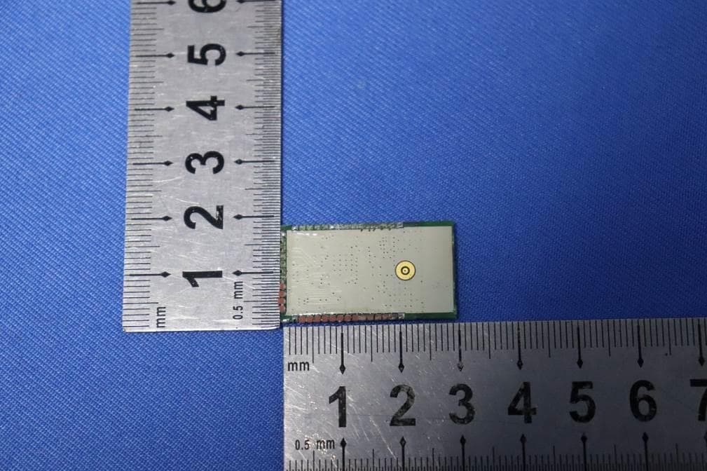
Click to zoom
Application Details
- Equipment Class
- DSS - Part 15 Spread Spectrum Transmitter
- Date of Grant
- Jun 29, 2021
- Application Purpose
- Original Equipment
- Date of Application
- Jun 29, 2021
- Equipment Note
- Bluetooth 5.0 Stereo Audio Module
- Frequency Range
- 2402.00000000 - 2480.00000000
- Country
- China
Documents & Files
Document Text
Text extracted from the exhibit documents filed with the FCC. Open a document above to read the original.
Users Manual
VTech proprietary and confidential VTech Communications LTD. R&D Department The document is VTech’s proprietary information, Please do not disclose to third party without VTech’s consent Ref. No.: 20210410 Version: 1.0 Date: 2021/04/10 Page 1 of 33 VTBM-A01 BT MODULE Bluetooth® 5.0 Stereo Audio Module Features: ■ Complete, Fully Certified, Embedded 2.4GHz Bluetooth®Version5.0 Module ■ Bluetooth Classic (BDR/EDR) ■ Firmware can be field upgradable via SPI ■ Compact surface mount module: 30 x 17 x 3mm³(cover changed) ■ Castellated surface mount pads for easy and reliable host PCB mounting ■ Perfect for Portable Battery Operated Devices ■ Audio-In / Out Operational: ■ Operating voltage: 3.2V to 5.0V ■ Temperature range: ‐40C to 85°C ■ Simple, SPI interface ■ Integrated crystal, internal voltage regulator, and matching circuitry ■ Multiple I/O pins for control and status RF/Analog: ■ Frequency: 2.402 to 2.480 GHz ■ Receive Sensitivity: ‐90 dBm (type) BDR receiver sensitivity ■ Power Output: class 1 / +9dBm max. ■ Connection Distance: >10m (free space and no interference) Integrated power control regulation: Audio processor: ■ Dual I²S outputs Supported sample rates of 8, 11.025,16, 22.05, 32,44.1, and 48kHz (DAC only) ■ I²S input, SPDIF input (uncompressed PCM only) Stereo codec with 1 microphone input , stereo audio DAC ■ USB audio ■ Stereo audio ADC with line input, stereo audio DAC ■ Support SCMS-T Auxiliary features: ■ Crystal oscillator with built-in digital trimming Physical interfaces: UART interface ■ USB 2.0 (full-speed) interface, including ■ USB charger detection ■ 4‑bit SPI flash memory interface ■ SPI interface for debug and programming ■ I²C master support ■ Up to 14 general-purpose PIOs ■ 3 LED drivers with PWM flasher independent of MCU VTech proprietary and confidential VTech Communications LTD. R&D Department The document is VTech’s proprietary information, Please do not disclose to third party without VTech’s consent Ref. No.: 20191009 Version: 01 Date: 09 Oct, 2019 Page 2 of 33 ■ 2 high-efficiency switch-mode regulators with 1.8 V and 1.35 V outputs direct from battery supply ■ 3.3 V linear regulator for USB supply ■ Low-voltage linear regulator for internal digital circuits ■ Low-voltage linear regulator for internal analog circuits ■ Power-on-reset detects low supply voltage ■ Power management for ultralow power mode Bluetooth features: ■ Bluetooth v5.0 specification support ■ A2DP v1.3.1 ■ AVRCP v1.6 ■ HFP v1.7 ■ QTIL's proximity pairing and QTIL's proximity connection Battery charger: ■ Lithium ion / Lithium polymer battery charger ■ Charger supports 4.20 V and 4.35 V cells ■ Instant-on function automatically selects the power supply between battery and USB, which enables operation even if the battery is fully discharged ■ Fast charging support □ Up to 200 mA with no external components □ Up to 500 mA with external pass transistor ■ Supports USB charger detection ■ Support for thermistor protection of battery pack Audio features: ■ SBC, and AAC audio codecs ■ Configurable Signal Detection to trigger events ■ 1 bank of up to 10-stage Speaker Parametric EQ ■ 6 banks of up to 5-stage User Parametric EQ for music enhancement ■ Qualcomm®meloD™ Expansion audio processing: 3D stereo widening ■ Compander to compress or expand the dynamic range of the audio ■ Post Mastering to improve DAC fidelity ■ Dual I²S outputs with crossover VTech proprietary and confidential VTech Communications LTD. R&D Department The document is VTech’s proprietary information, Please do not disclose to third party without VTech’s consent Ref. No.: 20191009 Version: 01 Date: 09 Oct, 2019 Page 3 of 33 1 Device overview The stereo module VTBM-A01 BT Module provides a complete 2.4GHz Bluetooth system, based on Qualcomm 3008 chip which is a single-chip radio and baseband IC for Bluetooth,2.4GHz systems including basic rate, EDR. The chip integrates Bluetooth 5.0 radio transceiver. Figure 1-1 shows the application block diagram. Figure 1-1: Block Diagram: The following depicts an example of VTBM-A01 BT Module operates as an independent system or connected to an MCU. Figure 1-1 1.1 Interface description VTBM-A01 pin diagram is shown in Figure 1-2. The pin descriptions are shown in Table 1-1 FIGURE 1-2: VTBM-A01 PIN DIAGRAM VTech proprietary and confidential VTech Communications LTD. R&D Department The document is VTech’s proprietary information, Please do not disclose to third party without VTech’s consent Ref. No.: 20191009 Version: 01 Date: 09 Oct, 2019 Page 4 of 33 Figure 1-2 TABLE 1-1: VTBM-A01 PIN DESCRIPTION PIN NO. Pin TYP Pin Name Description H1 P GND GND H2 O SPK_RN Speaker output negative, right H3 O SPK_RP Speaker output positive, right H4 I MIC_BN Line input negative, channel B H5 I MIC_BP Line input positive, channel B H6 O SPK_LN Speaker output negative, left H7 O SPK_LP Speaker output positive, left H8 AIO AIO[0] Analog programmable input line 0. H9 I/O PIO[4]/I2S1_WS/SPI_CS# Programmable input/output line 4./SPI_CS#/I2S1_WS H10 I/O PIO[16]/UART_RTS# Programmable input/output line 16./UART_RTS H11 I/O PIO[3]/I2S1_SD_OUT/SPI_MISO Programmable input/output line 3./SPI_MISO/I2S1_SD_OUT H12 SPI_MOSI SPI_MOSI SPI_MOSI: Debug SPI data input H13 I/O PIO[17]/UART_CTS# Programmable input/output line 17./UART_CTS H14 I/O PIO[5]/I2S1_SCK_SPI_CLK Programmable input/output line 5./SPI_CLK/I2S1_SCK H15 P GND GND H16 I RST Reset if low. Pull low for minimum 5 ms to cause a reset. H17 O LED[1] Open-drain output H18 O LED[0] Open-drain output H19 P VREGENABLE Regulator enable and multifunction button. A high input (tolerant to VBAT voltages) enables the on-chip regulators, which can then be latched on internally and the button used as a multifunction input. H20 P VCHG Charger input. H21 P VBAT Battery positive terminal. H22 P SMPS_1.8V 1.8V switch-mode power regulator output H23 P CHG_EXT External battery charger transistor base control when using external charger boost. Otherwise leave unconnected H24 I VBAT…
Text truncated - open the document above for the full version.
Users Manual
FCC regulatory compliance statement §15.19 Statement This device complies with Part 15 of the FCC Rules. Operation is subject to the following two conditions: (1) this device may not cause harmful interference, and (2) this device must accept any interference received, including interference that may cause undesired operation. §15.21 Information to user Warning: changes or modifications not expressly approved by the party responsible for compliance could void the user’s authority to operate the equipment. ⚫ List of applicable FCC rules: 47 CFR Part 15, Subpart C 15.203 47 CFR Part 15, Subpart C 15.205 47 CFR Part 15, Subpart C 15.207 47 CFR Part 15, Subpart C 15.209 47 CFR Part 15, Subpart C 15.247 47 CFR Part 2.1093 ⚫ Summarize the specific operational use conditions This module can be used in IOT devices, the input voltage to the module is nominally 3.2-5V. ⚫ Limited module procedures This module is not a limited module. ⚫ Trace antenna designs The antenna is not a trace antenna. ⚫ RF exposure considerations This Module complies with FCC radiation exposure limits set forth for an uncontrolled environment. This equipment should be installed and operated with a minimum distance of 20cm between the radiator and your body. This transmitter must not be co-located or operating in conjunction with any other antenna or transmitter. ⚫ Antennas If you desire to increase antenna gain and either change antenna type or use same antenna type certified, a Class II permissive change application is required to be filed by us, or you (host manufacturer) can take responsibility through the change in FCC ID (new application) procedure followed by a Class II permissive change application. ⚫ Label and compliance information Please notice that if the FCC identification number is not visible when the module is installed inside another device, then the outside of the device into which the module is installed must also display a label referring to the enclosed module. This exterior label can use wording such as the following: “Contains FCC ID: 2AZ2A-VTBMA01” any similar wording that expresses the same meaning may be used. § 15.19 Labelling requirements shall be complied on end user device. Labelling rules for special device, please refer to §2.925, § 15.19 (a)(5) and relevant KDB publications. For E-label, please refer to §2.935. ⚫ Information on test modes and additional testing requirements The OEM integrator is responsible for ensuring that the end-user has no manual instruction to remove or install module. The module is limited to installation in mobile application, a separate approval is required for all other operating configurations, including portable configurations with respect to §2.1093 and difference antenna configurations. Test software access to different test modes: Bluetooth test 3 (V2.6) Testing item, Frequencies, Transmit Power, Modulation Type can be selected on the test script instructions. ⚫ FCC other Parts, Part 15B Compliance Requirements for Host product manufacturer This modular transmitter is only FCC authorized for the specific rule parts listed on our grant, host product manufacturer is responsible for compliance to any other FCC rules that apply to the host not covered by the modular transmitter grant of certification. Host manufacturer in any case shall ensure host product which is installed and operating with the module is in compliant with Part 15B requirements. Please note that For a Class B or Class A digital device or peripheral, the instructions furnished the user manual of the end-user product shall include statement set out in §15.105 Information to the user or such similar statement and place it in a prominent location in the text of host product manual. Original texts as following: For Class B Note: This equipment has been tested and found to comply with the limits for a Class B digital device, pursuant to part 15 of the FCC Rules. These limits are designed to provide reasonable protection against harmful interference in a residential installation. This equipment generates, uses and can radiate radio frequency energy and, if not installed and used in accordance with the instructions, may cause harmful interference to radio communications. However, there is no guarantee that interference will not occur in a particular installation. If this equipment does cause harmful interference to radio or television reception, which can be determined by turning the equipment off and on, the user is encouraged to try to correct the interference by one or more of the following measures: —Reorient or relocate the receiving antenna. —Increase the separation between the equipment and receiver. —Connect the equipment into an outlet on a circuit different from that to which the receiver is connected. —Consult the dealer or an experienced radio/TV technician for help. For Class A Note: This equipment has been tested and found to comply with the limits for a Class A digital device, pursuant to part 15 of the FCC Rules. These limits are designed to provide reasonable protection against harmful interference when the equipment is operated in a commercial environment. This equipment generates, uses, and can radiate radio frequency energy and, if not installed and used in accordance with the instruction manual, may cause harmful interference to radio communications. Operation of this equipment in a residential area is likely to cause harmful interference in which case the user will be required to correct the interference at his own expense. ===================================================== ISED compliance statement This device contains licence-exempt transmitter(s)/receiver(s) that comply with Innovation, Science and Economic Development Canada’s licence-exempt RSS(s). Operation is subject to the following two conditions: (1) This device may not cause interference. (2) This device must accept any interference, including interference that may cause undesired operation of the device. L’émetteur/ré…
Text truncated - open the document above for the full version.
External Photos
SGS-CSTC Standards Technical Services Co., Ltd. Shenzhen Branch Page: 1 of 3 External Photos for SZCR2105020864AT FCC ID: 2AZ2A-VTBMA01 SGS-CSTC Standards Technical Services Co., Ltd. Shenzhen Branch Page: 2 of 3 1 EUT Constructional Details Dipole Antenna SGS-CSTC Standards Technical Services Co., Ltd. Shenzhen Branch Page: 3 of 3 PCB Antenna
ID Label/Location Info
Label Location: please see external photo RF shielding on page 1.
Internal Photos
SGS-CSTC Standards Technical Services Co., Ltd. Shenzhen Branch Page: 1 of 2 Internal Photos for SZCR2105020864AT FCC ID: 2AZ2A-VTBMA01 SGS-CSTC Standards Technical Services Co., Ltd. Shenzhen Branch Page: 2 of 2 1 EUT Constructional Details
RF Exposure Info
SGS-CSTC Standards Technical Services Co., Ltd. Shenzhen Branch Report No.: SZCR210502086402 Page: 1 of 6 Keny Xu EMC Laboratory Manager 1 Cover page SAR Evaluation Report Application No.: SZCR2105020864AT Applicant: VTech (Dongguan) Communications Ltd. Address of Applicant: Xia Ling Bei Management Zone, Liaobu Town, Dongguan City, Guangdong province, China. Manufacturer: VTech (Dongguan) Communications Ltd. Address of Manufacturer: Xia Ling Bei Management Zone, Liaobu Town, Dongguan City, Guangdong province, China. Factory: VTech (Dongguan) Communications Ltd. Address of Factory: Xia Ling Bei Management Zone, Liaobu Town, Dongguan City, Guangdong province, China. Equipment Under Test (EUT): EUT Name: Bluetooth 5.0 Stereo Audio Module Model No.: VTBM-A01 Trade mark: VTech FCC ID: 2AZ2A-VTBMA01 Standards: 47 CFR Part 1.1307 47 CFR Part 2.1093 KDB447498D01 General RF Exposure Guidance v06 Date of Receipt: 2021-05-06 Date of Test: 2021-05-10 to 2021-05-17 Date of Issue: 2021-07-02 Test Result : PASS* * In the configuration tested, the EUT complied with the standards specified above. SGS-CSTC Standards Technical Services Co., Ltd. Shenzhen Branch Report No.: SZCR210502086402 Page: 2 of 6 2 Version Revision Record Version Chapter Date Modifier Remark 01 2021-05-25 Original 02 2021-07-02 Update Antenna type New Authorized for issue by: Vincent Chen/Project Engineer Eric Fu/Reviewer SGS-CSTC Standards Technical Services Co., Ltd. Shenzhen Branch Report No.: SZCR210502086402 Page: 3 of 6 3 Contents Page 1 COVER PAGE ........................................................................................................................................ 1 2 VERSION ................................................................................................................................................ 2 3 CONTENTS ............................................................................................................................................ 3 4 GENERAL INFORMATION ..................................................................................................................... 4 4.1 GENERAL DESCRIPTION OF EUT ......................................................................................................... 4 4.2 TEST LOCATION ................................................................................................................................ 5 4.3 TEST FACILITY .................................................................................................................................. 5 4.4 DEVIATION FROM STANDARDS ............................................................................................................ 5 4.5 ABNORMALITIES FROM STANDARD CONDITIONS .................................................................................... 5 4.6 OTHER INFORMATION REQUESTED BY THE CUSTOMER .......................................................................... 5 5 SAR EVALUATION ................................................................................................................................. 6 5.1 RF EXPOSURE COMPLIANCE REQUIREMENT ........................................................................................ 6 5.1.1 Standard Requirement ................................................................................................................ 6 5.1.2 Limits .......................................................................................................................................... 6 5.1.3 EUT RF Exposure ....................................................................................................................... 6 SGS-CSTC Standards Technical Services Co., Ltd. Shenzhen Branch Report No.: SZCR210502086402 Page: 4 of 6 4 General Information 4.1 General Description of EUT Power supply: Powered by DC 3.2-5V Bluetooth Version: V5.0 classic Operation Frequency: 2402MHz to 2480MHz Modulation Type: GFSK, Pi/4DQPSK, 8DPSK Channel Spacing: 1MHz Number of Channels: 79 Antenna Type: PCB Antenna, Dipole Antenna Antenna Gain: PCB Antenna 1.73dBi, Dipole Antenna -1.07dBi SGS-CSTC Standards Technical Services Co., Ltd. Shenzhen Branch Report No.: SZCR210502086402 Page: 5 of 6 4.2 Test Location All tests were performed at: SGS-CSTC Standards Technical Services Co., Ltd. Shenzhen Branch No. 1 Workshop, M-10, Middle section, Science & Technology Park, Shenzhen, Guangdong, China 518057 Telephone: +86 (0) 755 2601 2053 Fax: +86 (0) 755 2671 0594 No tests were sub-contracted. 4.3 Test Facility The test facility is recognized, certified, or accredited by the following organizations: • A2LA (Certificate No. 3816.01) SGS-CSTC Standards Technical Services Co., Ltd., Shenzhen EMC Laboratory is accredited by the American Association for Laboratory Accreditation(A2LA). Certificate No. 3816.01. • VCCI The 3m Fully-anechoic chamber for above 1GHz, 10m Semi-anechoic chamber for below 1GHz, Shielded Room for Mains Port Conducted Interference Measurement and Telecommunication Port Conducted Interference Measurement of SGS-CSTC Standards Technical Services Co., Ltd. have been registered in accordance with the Regulations for Voluntary Control Measures with Registration No.: G-20026, R-14188, C-12383 and T-11153 respectively. • FCC –Designation Number: CN1178 SGS-CSTC Standards Technical Services Co., Ltd., Shenzhen EMC Laboratory has been recognized as an accredited testing laboratory. Designation Number: CN1178. Test Firm Registration Number: 406779. • Innovation, Science and Economic Development Canada SGS-CSTC Standards Technical Services Co., Ltd., Shenzhen EMC Laboratory has been recognized by ISED as an accredited testing laboratory. CAB identifier: CN0006. IC#: 4620C. 4.4 Deviation from Standards None. 4.5 Abnormalities from Standard Conditions None. 4.6 Other Information Requested by the Customer None. SGS-CSTC Standards Technical Services Co., Ltd. Shenzhen Branch Report No.: SZCR210502086402 Page: 6 of 6 5 SAR Eva…
Text truncated - open the document above for the full version.
Test Report
SGS-CSTC Standards Technical Services Co., Ltd. Shenzhen Branch Report No.: SZCR210502086401 Page: 1 of 101 Keny Xu EMC Laboratory Manager TEST REPORT Application No.: SZCR2105020864AT Applicant: VTech (Dongguan) Communications Ltd. Address of Applicant: Xia Ling Bei Management Zone, Liaobu Town, Dongguan City, Guangdong province, China. Manufacturer: VTech (Dongguan) Communications Ltd. Address of Manufacturer: Xia Ling Bei Management Zone, Liaobu Town, Dongguan City, Guangdong province, China. Factory: VTech (Dongguan) Communications Ltd. Address of Factory: Xia Ling Bei Management Zone, Liaobu Town, Dongguan City, Guangdong province, China. Equipment Under Test (EUT): EUT Name: Bluetooth 5.0 Stereo Audio Module Model No.: VTBM-A01 Trade Mark: VTech FCC ID: 2AZ2A-VTBMA01 Standard(s) : 47 CFR Part 15, Subpart C 15.247 Date of Receipt: 2021-05-06 Date of Test: 2021-05-10 to 2021-05-19 Date of Issue: 2021-07-02 Test Result: Pass* * In the configuration tested, the EUT complied with the standards specified above. SGS-CSTC Standards Technical Services Co., Ltd. Shenzhen Branch Report No.: SZCR210502086401 Page: 2 of 101 Revision Record Version Chapter Date Modifier Remark 01 2021-05-25 Original 02 2021-07-02 Update the Antenna type New Authorized for issue by: Vincent Chen/Project Engineer Eric Fu/Reviewer SGS-CSTC Standards Technical Services Co., Ltd. Shenzhen Branch Report No.: SZCR210502086401 Page: 3 of 101 2 Test Summary Radio Spectrum Technical Requirement Item Standard Method Requirement Result Antenna Requirement 47 CFR Part 15, Subpart C 15.247 N/A 47 CFR Part 15, Subpart C 15.203 & 15.247(b)(4) Pass Other requirements Frequency Hopping Spread Spectrum System Hopping Sequence N/A 47 CFR Part 15, Subpart C 15.247(a)(1),(g),(h) Pass Radio Spectrum Matter Part Item Standard Method Requirement Result Conducted Peak Output Power 47 CFR Part 15, Subpart C 15.247 ANSI C63.10 (2013) Section 7.8.5 47 CFR Part 15, Subpart C 15.247(b)(1) Pass 20dB Bandwidth ANSI C63.10 (2013) Section 7.8.7 47 CFR Part 15, Subpart C 15.247(a)(1) Pass Carrier Frequencies Separation ANSI C63.10 (2013) Section 7.8.2 47 CFR Part 15, Subpart C 15.247a(1) Pass Hopping Channel Number ANSI C63.10 (2013) Section 7.8.3 47 CFR Part 15, Subpart C 15.247a(1)(iii) Pass Dwell Time ANSI C63.10 (2013) Section 7.8.4 47 CFR Part 15, Subpart C 15.247a(1)(iii) Pass Conducted Band Edges Measurement ANSI C63.10 (2013) Section 7.8.6 47 CFR Part 15, Subpart C 15.247(d) Pass Conducted Spurious Emissions ANSI C63.10 (2013) Section 7.8.8 47 CFR Part 15, Subpart C 15.247(d) Pass Radiated Emissions which fall in the restricted bands ANSI C63.10 (2013) Section 6.10.5 47 CFR Part 15, Subpart C 15.205 & 15.209 Pass Radiated Spurious Emissions Below 1GHz ANSI C63.10 (2013) Section 6.4,6.5 47 CFR Part 15, Subpart C 15.205 & 15.209 Pass Radiated Spurious Emissions Above 1GHz ANSI C63.10 (2013) Section 6.6 47 CFR Part 15, Subpart C 15.205 & 15.209 Pass Emission Part Item Standard Method Requirement Result Conducted Emissions at AC Power Line (150kHz-30MHz) 47 CFR Part 15, Subpart C 15.247 ANSI C63.10 (2013) Section 6.2 47 CFR Part 15, Subpart C 15.207 Pass SGS-CSTC Standards Technical Services Co., Ltd. Shenzhen Branch Report No.: SZCR210502086401 Page: 4 of 101 3 Contents Page 1 COVER PAGE ..................................................................................................................................... 1 2 TEST SUMMARY ................................................................................................................................. 3 3 CONTENTS ......................................................................................................................................... 4 4 GENERAL INFORMATION .................................................................................................................. 6 4.1 DETAILS OF E.U.T. ......................................................................................................................... 6 4.2 DESCRIPTION OF SUPPORT UNITS .................................................................................................... 6 4.3 MEASUREMENT UNCERTAINTY ......................................................................................................... 6 4.4 TEST LOCATION ............................................................................................................................. 7 4.5 TEST FACILITY ............................................................................................................................... 7 4.6 DEVIATION FROM STANDARDS ......................................................................................................... 7 4.7 ABNORMALITIES FROM STANDARD CONDITIONS ................................................................................. 7 5 EQUIPMENT LIST ............................................................................................................................... 8 6 RADIO SPECTRUM TECHNICAL REQUIREMENT ............................................................................12 6.1 ANTENNA REQUIREMENT ................................................................................................................12 6.1.1 Test Requirement: ..................................................................................................................12 6.1.2 Conclusion ..............................................................................................................................12 6.2 OTHER REQUIREMENTS FREQUENCY HOPPING SPREAD SPECTRUM SYSTEM HOPPING SEQUENCE ........13 6.2.1 Test Requirement: ..................................................................................................................13 7 RADIO SPECTRUM MATTER TEST RESULTS .................................................................................15 7.1 CONDUCTED PEAK OUTPUT POWER .................................................................................…
Text truncated - open the document above for the full version.
Test Report
SGS-CSTC Standards Technical Services Co., Ltd. Shenzhen Branch Report No.: SZCR210502086401 Page: 79 of 101 5. Time of Occupancy (Dwell Time) 5.1 Test Result Test Mode Packet Type TX Type ANT No. Duration of Single Pulse (ms) Obeserv ation Period (s) Num of Pulse in Observation Period Dwell Time (ms) Limits (ms) Verdict GFSK DH1 SISO 1 0.409 31.6 320 130.880 ≤400 PASS DH3 SISO 1 1.663 31.6 160 266.080 ≤400 PASS DH5 SISO 1 2.915 31.6 106 308.990 ≤400 PASS Pi/4DQ PSK 2DH1 SISO 1 0.423 31.6 320 135.360 ≤400 PASS 2DH3 SISO 1 1.682 31.6 160 269.120 ≤400 PASS 2DH5 SISO 1 2.924 31.6 107 312.868 ≤400 PASS 8DPSK 3DH1 SISO 1 0.423 31.6 320 135.360 ≤400 PASS 3DH3 SISO 1 1.681 31.6 160 268.960 ≤400 PASS 3DH5 SISO 1 2.925 31.6 106 310.050 ≤400 PASS 5.2 Test Graph SGS-CSTC Standards Technical Services Co., Ltd. Shenzhen Branch Report No.: SZCR210502086401 Page: 80 of 101 SGS-CSTC Standards Technical Services Co., Ltd. Shenzhen Branch Report No.: SZCR210502086401 Page: 81 of 101 SGS-CSTC Standards Technical Services Co., Ltd. Shenzhen Branch Report No.: SZCR210502086401 Page: 82 of 101 SGS-CSTC Standards Technical Services Co., Ltd. Shenzhen Branch Report No.: SZCR210502086401 Page: 83 of 101 SGS-CSTC Standards Technical Services Co., Ltd. Shenzhen Branch Report No.: SZCR210502086401 Page: 84 of 101 SGS-CSTC Standards Technical Services Co., Ltd. Shenzhen Branch Report No.: SZCR210502086401 Page: 85 of 101 SGS-CSTC Standards Technical Services Co., Ltd. Shenzhen Branch Report No.: SZCR210502086401 Page: 86 of 101 SGS-CSTC Standards Technical Services Co., Ltd. Shenzhen Branch Report No.: SZCR210502086401 Page: 87 of 101 SGS-CSTC Standards Technical Services Co., Ltd. Shenzhen Branch Report No.: SZCR210502086401 Page: 88 of 101 SGS-CSTC Standards Technical Services Co., Ltd. Shenzhen Branch Report No.: SZCR210502086401 Page: 89 of 101 6. Unwanted Emissions in Non-restricted Frequency Bands 6.1 Test Result Test Mode Frequency (MHz) TX Type ANT No. Spurious Conducted Emission (dBm) Limits (dBm) Verdict GFSK 2402 SISO 1 Refer to test graph -16.79 PASS 2441 SISO 1 Refer to test graph -16.79 PASS 2480 SISO 1 Refer to test graph -16.79 PASS Hopping SISO 1 Refer to test graph -16.79 PASS Pi/4DQPSK 2402 SISO 1 Refer to test graph -22.12 PASS 2441 SISO 1 Refer to test graph -22.12 PASS 2480 SISO 1 Refer to test graph -22.12 PASS Hopping SISO 1 Refer to test graph -22.12 PASS 8DPSK 2402 SISO 1 Refer to test graph -22.11 PASS 2441 SISO 1 Refer to test graph -22.11 PASS 2480 SISO 1 Refer to test graph -22.11 PASS Hopping SISO 1 Refer to test graph -22.11 PASS 6.2 Test Graph SGS-CSTC Standards Technical Services Co., Ltd. Shenzhen Branch Report No.: SZCR210502086401 Page: 90 of 101 SGS-CSTC Standards Technical Services Co., Ltd. Shenzhen Branch Report No.: SZCR210502086401 Page: 91 of 101 SGS-CSTC Standards Technical Services Co., Ltd. Shenzhen Branch Report No.: SZCR210502086401 Page: 92 of 101 SGS-CSTC Standards Technical Services Co., Ltd. Shenzhen Branch Report No.: SZCR210502086401 Page: 93 of 101 SGS-CSTC Standards Technical Services Co., Ltd. Shenzhen Branch Report No.: SZCR210502086401 Page: 94 of 101 SGS-CSTC Standards Technical Services Co., Ltd. Shenzhen Branch Report No.: SZCR210502086401 Page: 95 of 101 SGS-CSTC Standards Technical Services Co., Ltd. Shenzhen Branch Report No.: SZCR210502086401 Page: 96 of 101 SGS-CSTC Standards Technical Services Co., Ltd. Shenzhen Branch Report No.: SZCR210502086401 Page: 97 of 101 SGS-CSTC Standards Technical Services Co., Ltd. Shenzhen Branch Report No.: SZCR210502086401 Page: 98 of 101 SGS-CSTC Standards Technical Services Co., Ltd. Shenzhen Branch Report No.: SZCR210502086401 Page: 99 of 101 SGS-CSTC Standards Technical Services Co., Ltd. Shenzhen Branch Report No.: SZCR210502086401 Page: 100 of 101 SGS-CSTC Standards Technical Services Co., Ltd. Shenzhen Branch Report No.: SZCR210502086401 Page: 101 of 101 - End of the Report -
Test Setup Photos
SGS-CSTC Standards Technical Services Co., Ltd. Shenzhen Branch Page: 1 of 4 Setup Photos for SZCR2105020864AT FCC ID: 2AZ2A-VTBMA01 SGS-CSTC Standards Technical Services Co., Ltd. Shenzhen Branch Page: 2 of 4 1 Photographs Conducted Emissions at AC Power Line (150kHz-30MHz) Dipole Antenna: PCB Antenna: SGS-CSTC Standards Technical Services Co., Ltd. Shenzhen Branch Page: 3 of 4 Radiated Spurious Emissions Below 1GHz Dipole Antenna: PCB Antenna: SGS-CSTC Standards Technical Services Co., Ltd. Shenzhen Branch Page: 4 of 4 Radiated Spurious Emissions Above 1GHz Dipole Antenna: PCB Antenna:
Contact Information
Applicant
Lily Zhang(Compliance Engineer)
Technical Contact
SGS-CSTC Standards Technical Services Co., Ltd.Keny Xu
[email protected]+8675525328629
No.1 Workshop, M-10, Middle Section, · Shenzhen · China
Test Firm
SGS-CSTC Standards Technical Services Co., LtdDerek Yang
[email protected]+86 0135 6484 8721
Technical Specifications
| # | Rule Parts | Frequency Range | Power Output |
|---|---|---|---|
| 1 | 15C | 2.40 GHz - 2.48 GHz | 2.40 mW |
Other Applications from VTech (Dongguan) Communications Limited
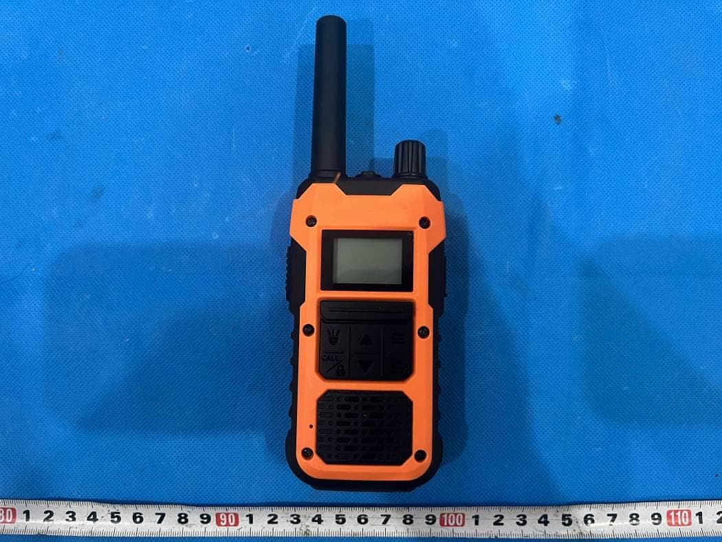
2AZ2A-VTR3320
Apr 30, 2026EXTREME GMRS
Equipment Class
TNF - Licensed Non-Broadcast Transmitter Held to Face
2AZ2A-VTR3311
Feb 13, 2026ADVENTURE FRS
Equipment Class
FRF - Part 95 Family Radio Face Held Transmitter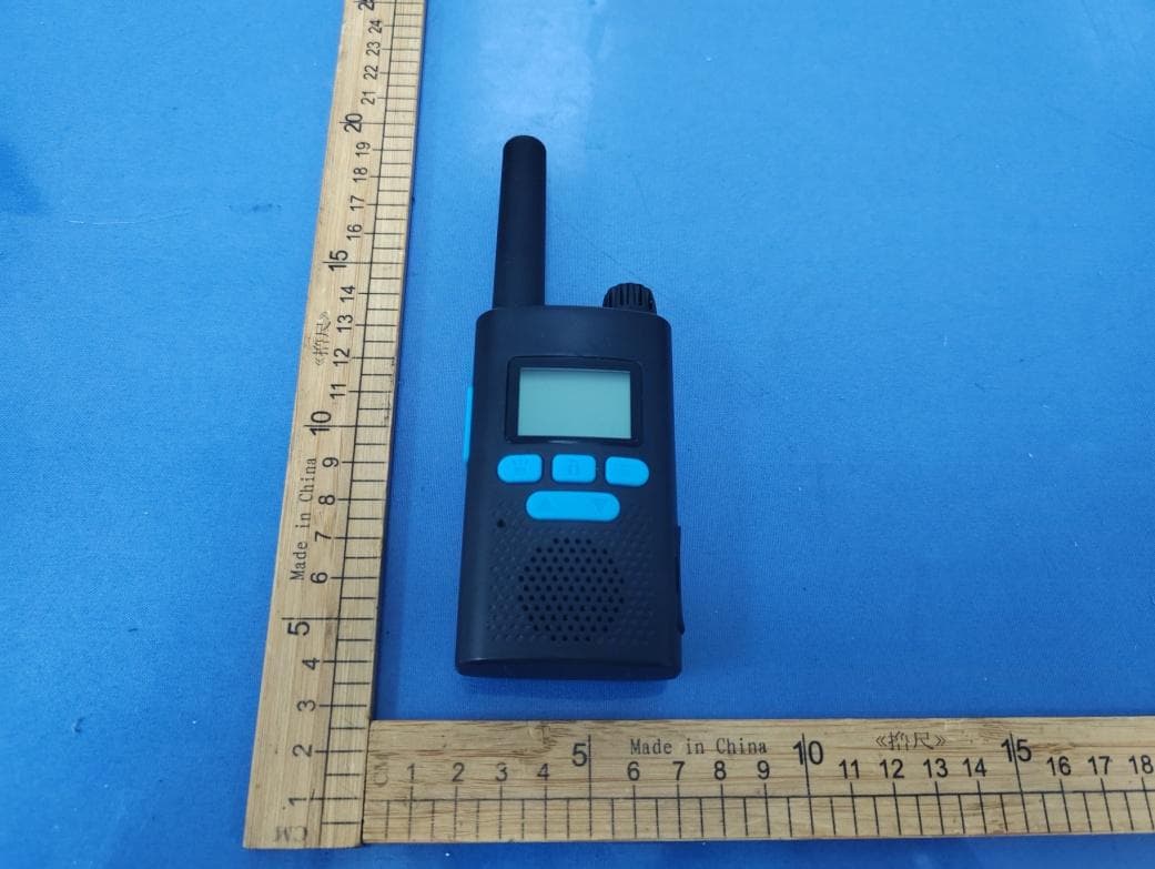
2AZ2A-VTR3310
Feb 13, 2026ESSENTIAL FRS
Equipment Class
FRF - Part 95 Family Radio Face Held Transmitter