2AZDW-AML550Communication Module
AM TELECOM Co.,Ltd.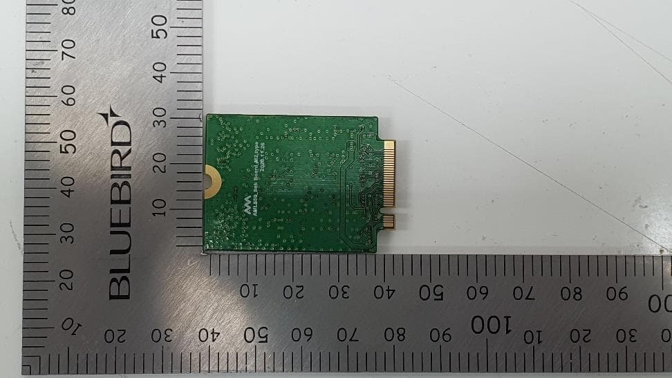
Click to zoom
Application Details
- Equipment Class
- PCB - PCS Licensed Transmitter
- Date of Grant
- May 01, 2021
- Application Purpose
- Original Equipment
- Date of Application
- Apr 29, 2021
- Equipment Note
- Communication Module
- Frequency Range
- 821.50000000 - 824.00000000
- Company
- AM TELECOM Co.,Ltd.
- Country
- South Korea
Documents & Files
Document Text
Text extracted from the exhibit documents filed with the FCC. Open a document above to read the original.
Users Manual
Rev 0.1 2021.04 AM TELECOM Communication Module AML550 Hardware User Guide 2 Limitations of Liability This user guide is provided “as is” and the recipient of the user guide shall endorse all risks arising from its use. In no event shall AM TELECOM has any responsibility for any damages if the product(s) has been improperly stored, installed, used or maintained, or if it has been made under any unauthorized modifications, adjustments and/or repairs to such product(s). IN NO EVENT WILL AM TELECOM OR ITS AFFILIATES BE LIABLE FOR ANY LOST PROFITS, LOST SAVINGS OR INCIDENTAL, INDIRECT, SPECIAL OR CONSEQUENTIAL DAMAGES, ARISING OUT OF USE OR INABILITY TO USE THE PRODUCT, EVEN IF ADVISED OF THE POSSIBILITY OF SUCH DAMAGES. SOME STATES DO NOT ALLOW THE LIMITATION OR EXCLUSION OF LIABILITY FOR INCIDENTAL OR CONSEQUENTIAL DAMAGES SO THE ABOVE LIMITATION OR EXCLUSION MAY NOT APPLY. Copyright ⓒ AM TELECOM Co.,Ltd, 2021 Transmittal, reproduction, dissemination and(or) editing of this document as well as utilization of its contents and communication thereof to others without express authorization are prohibited. Offenders will be held liable for payment of damages. All rights are reserved. 3 ■ Revision History Version Date Description Editor Draft 2021.04.01 Initial release M.S KANG 4 Contents INTRODUCTION ....................................................................................................................... 6 1. SYSTEM SPECIFICATION .................................................................................................... 7 1.1. PHYSICAL FEATURE ........................................................................................ 7 1.2. MODEM SPECIFICATION ................................................................................... 8 1.2.1. MODEM FREQUENCY SPECIFICATION ................................................................... 8 1.2.2. ELECTRICAL SPECIFICATION ............................................................................. 8 1.2.3. ENVIRONMENT SPECIFICATION ......................................................................... 9 1.3. RF SPECIFICATIONS ..................................................................................... 10 1.3.1. RX/TX FREQUENCY SPECIFICATION - LTE MODE ................................................. 10 1.3.2. RX/TX FREQUENCY SPECIFICATION - WCDMA MODE .......................................... 11 1.3.3. RX/TX FREQUENCY SPECIFICATION - GSM MODE ................................................ 11 1.4. SYSTEM BLOCK ............................................ 오류! 책갈피가 정의되어 있지 않습니다. 2. INTERFACE CONNECTOR .................................................................................................. 12 2.1. PIN ASSIGNMENT ......................................................................................... 12 2.2. PIN DESCRIPTION ....................................................................................... 13 3. MODEM INTERFACE DESCRIPTION ................................................................................... 20 3.1. POWER SUPPLY ........................................................................................... 20 3.2. USB INTERFACE .......................................................................................... 21 3.3. USIM INTERFACE ........................................................................................ 21 3.4. UART INTERFACE ........................................................................................ 22 3.5. WLAN INTERFACE ....................................................................................... 22 3.6. ETHERNET INTERFACE ................................................................................... 23 3.7. IN/OUT INTERFACE ..................................................................................... 24 3.7.1. POWER_KEY ............................................................................................ 24 3.7.2. RESET_KEY ............................................................................................. 25 3.7.3. WAKE_UP ................................................................................................ 25 3.7.4. USB_DISABLE ......................................................................................... 26 3.7.5. READY..................................................................................................... 26 3.8. DEBUG INTERFACE ....................................................................................... 26 3.9. ANTENNA .................................................................................................. 26 3.10. RESERVED ................................................................................................. 27 4. CURRENT CONSUMPTION ................................................................................................. 29 5. SIGNAL TIMING ............................................................. 오류! 책갈피가 정의되어 있지 않습니다. 5.1. POWER ON SEQUENCE ................................... 오류! 책갈피가 정의되어 있지 않습니다. 5.2. POWER OFF SEQUENCE .................................. 오류! 책갈피가 정의되어 있지 않습니다. 5.3. RESTART SEQUENCE ...................................... 오류! 책갈피가 정의되어 있지 않습니다. 5.4. RECOVERT PROCESS ..................................... 오류! 책갈피가 정의되어 있지 않습니다. 5 6. RF DESIGN GUIDE ............................................................................................................ 29 6.1. ANTENNA RF DESIGN GUIDE .......................................................................... 29 6.2. RF LINE DESIGN GUIDE ................................................................................ 31 7. PCB LAYOUT GUIDE ......................................................................................................... 32 8. SOLDER REFLOW PROFILE ............................................................................................... 33 9. CAUTIONS ....................................................…
Text truncated - open the document above for the full version.
Users Manual
Rev 0.1 2021.04 AM TELECOM Communication Module AMM5500 Hardware User Guide 2 Limitations of Liability This user guide is provided “as is” and the recipient of the user guide shall endorse all risks arising from its use. In no event shall AM TELECOM has any responsibility for any damages if the product(s) has been improperly stored, installed, used or maintained, or if it has been made under any unauthorized modifications, adjustments and/or repairs to such product(s). IN NO EVENT WILL AM TELECOM OR ITS AFFILIATES BE LIABLE FOR ANY LOST PROFITS, LOST SAVINGS OR INCIDENTAL, INDIRECT, SPECIAL OR CONSEQUENTIAL DAMAGES, ARISING OUT OF USE OR INABILITY TO USE THE PRODUCT, EVEN IF ADVISED OF THE POSSIBILITY OF SUCH DAMAGES. SOME STATES DO NOT ALLOW THE LIMITATION OR EXCLUSION OF LIABILITY FOR INCIDENTAL OR CONSEQUENTIAL DAMAGES SO THE ABOVE LIMITATION OR EXCLUSION MAY NOT APPLY. Copyright ⓒ AM TELECOM Co.,Ltd, 2021 Transmittal, reproduction, dissemination and(or) editing of this document as well as utilization of its contents and communication thereof to others without express authorization are prohibited. Offenders will be held liable for payment of damages. All rights are reserved. 3 ■ Revision History Version Date Description Editor Draft 2021.04.01 Initial release M.S KANG 4 Contents INTRODUCTION ....................................................................................................................... 6 1. SYSTEM SPECIFICATION .................................................................................................... 7 1.1. PHYSICAL FEATURE ........................................................................................ 7 1.2. INTERFACE PARTS SPECIFICATION ...................................................................... 8 1.2.1. Coaxial RF connector .............................................................................. 8 1.2.2. Host interface connector ......................................................................... 8 1.3. MODEM SPECIFICATION ................................................................................... 9 1.3.1. Modem Frequency specification .............................................................. 9 1.3.2. Electrical Specification .......................................................................... 10 1.3.3. Environment Specification .................................................................... 11 1.4. RF SPECIFICATIONS ..................................................................................... 12 1.4.1. RX/TX frequency specification - LTE mode ............................................ 12 1.4.2. RX/TX frequency specification - WCDMA mode ...................................... 13 1.4.3. RX/TX frequency specification - GSM mode ........................................... 13 1.5. SYSTEM BLOCK ............................................ 오류! 책갈피가 정의되어 있지 않습니다. 2. INTERFACE CONNECTOR .................................................................................................. 14 2.1. PIN ASSIGNMENT ......................................................................................... 14 2.2. PIN DESCRIPTION ....................................................................................... 15 3. MODEM INTERFACE DESCRIPTION ................................................................................... 18 3.1. POWER SUPPLY ........................................................................................... 18 3.2. USB INTERFACE .......................................................................................... 18 3.3. USIM INTERFACE ........................................................................................ 19 3.4. UART INTERFACE ........................................................................................ 19 3.5. WLAN INTERFACE ....................................................................................... 20 3.6. ETHERNET INTERFACE ................................................................................... 20 3.7. IN/OUT INTERFACE ..................................................................................... 21 3.7.1. POWER_KEY ............................................................................................ 21 3.7.2. RESET_KEY ............................................................................................. 23 3.7.3. WAKE_UP ................................................................................................ 23 3.7.4. USB_DISABLE ......................................................................................... 24 3.7.5. READY..................................................................................................... 24 3.8. RESERVED ................................................................................................. 24 4. CURRENT CONSUMPTION ................................................................................................. 25 5. SIGNAL TIMING ............................................................. 오류! 책갈피가 정의되어 있지 않습니다. 5.1. POWER ON SEQUENCE ................................... 오류! 책갈피가 정의되어 있지 않습니다. 5.2. POWER OFF SEQUENCE .................................. 오류! 책갈피가 정의되어 있지 않습니다. 5.3. RESTART SEQUENCE ...................................... 오류! 책갈피가 정의되어 있지 않습니다. 5 6. MECHANICAL DESIGN GUIDE ........................................................................................... 25 6.1. PCB LAYOUT GUIDE ...................................................................................... 25 6.2. INSERT NUT ............................................................................................... 26 6.3. SCREW ...................................................................................................... 26 7. CAUTIONS ....................................................................................................................... 27 7.1. SAFETY PRECAUTIONS ..................................................…
Text truncated - open the document above for the full version.
Cover Letter(s)
CONFIDENTIALITY REQUEST Federal Communication Commission Equipment Authorization Division, Application Processing Branch 7435 Oakland Mills Road Columbia, MD 21048 April 27 th , 2021 TO WHOM IT MAY CONCERN Pursuant to Paragraphs §0.457 and 0.459 of the Commission’s Rules (47 C.F.R.) and Section §552(b)(4) of the Freedom of Information Act, AM TELECOM Co., Ltd. requests confidentiality for the following products: FCC ID Number Product Title/Model 2AZDW-AML550 AMM5500, AML550 The following exhibits contain trade secrets and proprietary information that could be of benefit to our competitors regarding the design of our product. This material is not customarily available to the general public and we request that it be withheld from public inspection. We request that the following information submitted be held permanent confidential treatment. Permanent Confidential Request - Schematics - Block diagram - Tune up - Part List - Operational description We request that the following information submitted be held short-term confidential treatment for 180 days. Short- term Confidential Request - Internal photo - External photo - User’s manual - Set up photo If you have any questions, please feel free to contact me at the address shown below. Best regards, Name: Sang Muk Han Title: Team Manager E-mail: [email protected] Company name: AM TELECOM Co., Ltd.
Cover Letter(s)
Date: 19th of November, 2020 Federal Communications Commission 7435 Oakland Mills Road Columbia MD 21046 c.c. UL Verification Services Inc. (formerly UL CCS) Certification Division 47173 Benicia Street Fremont, CA 94538, USA To whom it may concern: I, the undersigned, hereby authorize UL-Korea and hereafter referred to as ULK, to act on our behalf in all manners relating to application for equipment authorization, including signing of all documents relating to these matters. Any and all acts carried out by UL-Korea on our behalf shall have the same effect as acts of our own. I, the undersigned, hereby certify that we are not subject to a denial of federal benefits, that includes FCC benefits, pursuant to Section 5301 of the Anti-Drug Abuse Act of 1988, 21 U.S.C. 853(a). In authorizing ULK as our agent, we still recognize that we are responsible to: a) comply with the relevant provisions of the certification program; b) make all necessary arrangements for the conduct of the evaluation, including provision for examining documentation and access to all areas, records (including internal audit reports) and personnel for the purposes of evaluation (e.g. testing, inspection, assessment, surveillance, reassessment) and resolution of complaints; c) make claims regarding certification only in respect of the scope for which certification has been granted; d) do not use our product certification in such a manner as to bring the Certification Division into disrepute and not make any statement regarding our product certification which the Certification Division may consider misleading or unauthorized; e) upon suspension or cancellation of certification, discontinue use of all advertising matter that contains any reference thereto and return any certification documents as required by the Certification Division; f) use certification only to indicate the products are certified as being in conformity with specified standards; g) endeavor to ensure that no certificate or report nor any part thereof is used in a misleading manner; h) ensure that any reference to our product certification in communication media such as documents, brochures or advertising, complies with the requirements of the Certification Division; i) keep a record of all complaints made known to the us relating to the product’s compliance with requirements of the relevant standard and to make these records available to the Certification Division when requested; j) take appropriate action with respect to such complaints and any deficiencies found in products or services that affect compliance with the requirements for certification; k) document the actions taken. This authorization is valid until further written notice from the applicant. Sincerely Yours, Name: Sang Muk Han Title: Team Manager E-mail: [email protected] Company name: AM TELECOM Co., Ltd. REMARK: 1. This authorization letter will be sent along with your application when filing with the Certification Division. 2. Please follow the format and type it on company letterhead and send original to us. 3. Authorized signature must be in agreement with grantee code contact in FCC database.
Cover Letter(s)
AM TELECOM Co., Ltd. 608, Yatap Leaders Building, 42, Jangmi-ro, Bundang-gu, Seongnam-si, Gyeonggi-do, 13496, South Korea UL Verification Services Inc. 47173 Benicia Street Fremont, CA 94538, USA April 6, 2021 Modular Approval Attestation for LTE Module Applicant: AM TELECOM Co., Ltd. FCC ID: 2AZDW-AML550 No. FCC requirements EUT 1 Have its own RF shielding RF Block shielded by Metal Case 2 Have buffered modulation/data inputs (if such inputs are provided), Yes, the module has buffered data input. 3 The modular transmitter must have its own power supply regulation. We used self own power supply regulation. 4 Meet the antenna requirements of section 15.203 This module uses unique connector (Type: MHF ) This module meets the antenna requirements of section 15.203 5 Be tested in a stand-alone configuration, i.e., the antenna, AC or DC power and data input/output lines must be connected to the module but, the module must not be inside another case during testing Yes, the EUT (module) was tested a stand-alone configuration. 6 Be labeled with its own FCC ID number, and if the FCC ID is not visible when the module is installed inside another device, then the outside of the device into which the module is installed must also display a label referring to the enclosed module. The proposed FCC ID label format is to be placed on the module. If FCC ID label is not visible when module is install into the system, “Contains FCC ID: 2AZDW-AML550” shall be placed on the outside of final product. 7 The modular transmitter is manufactured so that the user can not influence the operation of the transmitter that will operate outside of the scope of the regulations. It complies with specific rules or operating requirements. And instruction is included User manual. 8 Address compliance with the Commission`s RF exposure limits in Sections 1.1310 and 2.1093. In addition, spread spectrum transmitters operation under Section 15.247 are required to address RF exposure compliance in accordance with Section 15.247(b)(4) The exposure condition of this module is compliant with the requirements. Please refer to MPE calculation. Sincerely, Name : Han, Mr. Sang Muk Title : Team Manager
Cover Letter(s)
ID Letter (Declare of Antenna Gain) FCC ID: 2AZDW-AML550 / IC: 27086-AML550 Model: AMM5500, AML550 These models are LTE/WCDMA/GSM module. This device is to be used only for mobile and fixed application. For the correct use of these modules, we declare the maximum antenna gain to meet ERP/EIRP power limit and RF exposure compliance. Frequency Band 700 MHz 800 MHz 1700 MHz 1900 MHz 2500 MHz Max. Gain (dBi) 6.6 5.6 5.0 3.5 9.0 Note: Max. Gain is antenna gain included cable loss. 1. Max Gain (dBi) to comply @20cm with MPE Frequency Output Power Note 1 Mode Duty Cycle Frame AV Output power (W) MPE Limit (mW/cm 2 ) ISED Limit (mW/cm 2 ) Max Gain (dBi) to comply @20cm with FCC MPE Max Gain (dBi) to comply @20cm with ISED MPE MHz dBm W 699.7 24.00 0.251 LTE 12 100.0% 0.251 0.466 0.230 9.7 6.6 824.2 33.50 2.239 GSM 850 12.5% 0.280 0.549 0.258 9.9 6.7 824.2 31.50 1.413 GSM 850 25.0% 0.353 0.549 0.258 8.9 5.6 824.2 29.50 0.891 GSM 850 37.5% 0.334 0.549 0.258 9.2 5.9 826.4 25.00 0.316 WCDMA 5 100.0% 0.316 0.551 0.258 9.4 6.1 814.7 24.00 0.251 LTE 26 100.0% 0.251 0.543 0.256 10.4 7.1 1712.4 25.00 0.316 WCDMA 4 100.0% 0.316 1.000 0.425 12.0 8.3 1710.7 24.00 0.251 LTE 4 100.0% 0.251 1.000 0.424 13.0 9.3 1850.2 29.50 0.891 GSM 1900 12.5% 0.111 1.000 0.448 16.5 13.1 1850.2 28.00 0.631 GSM 1900 25.0% 0.158 1.000 0.448 15.0 11.5 1850.2 27.50 0.562 GSM 1900 37.5% 0.211 1.000 0.448 13.8 10.3 1852.4 25.00 0.316 WCDMA 2 100.0% 0.316 1.000 0.448 12.0 8.5 1850.7 24.00 0.251 LTE 2 100.0% 0.251 1.000 0.448 13.0 9.5 2502.5 24.00 0.251 LTE 7 100.0% 0.251 1.000 0.550 13.0 10.4 Note 1: Output Power is maximum power and includes tune-up tolerances. 2. Max Gain (dBi) to comply with Rule Frequency Output Power Note 1 Mode Rule Part Limits (W) Max Gain (dBi) to comply with Rule MHz dBm W Rule Limit (ERP) Limit (EIRP) 699.7 24.00 0.251 LTE 12 27 3.00 12.9 824.2 33.50 2.239 GSM 850 22H 7.00 7.1 824.2 31.50 1.413 GSM 850 22H 7.00 9.1 824.2 29.50 0.891 GSM 850 22H 7.00 11.1 826.4 25.00 0.316 WCDMA 5 22H 7.00 15.6 814.7 24.00 0.251 LTE 26 22H 7.00 16.6 1712.4 25.00 0.316 WCDMA 4 27 1.00 5.0 1710.7 24.00 0.251 LTE 4 27 1.00 6.0 1850.2 29.50 0.891 GSM 1900 24E 2.00 3.5 1850.2 28.00 0.631 GSM 1900 24E 2.00 5.0 1850.2 27.50 0.562 GSM 1900 24E 2.00 5.5 1852.4 25.00 0.316 WCDMA 2 24E 2.00 8.0 1850.7 24.00 0.251 LTE 2 24E 2.00 9.0 2502.5 24.00 0.251 LTE 7 27M 2.00 9.0 Note 1: Output Power is maximum power and includes tune-up tolerances 3. Max Gain (dBi) to comply with Rule and MPE Frequency Mode Max Gain (dBi) to comply @20cm with FCC MPE Max Gain (dBi) to comply @20cm with ISED MPE Max Gain (dBi) to comply with Rule Max Gain (dBi) to comply MHz 699.7 LTE 12 9.7 6.6 12.9 6.6 824.2 GSM 850 9.9 6.7 7.1 5.6 824.2 GSM 850 8.9 5.6 9.1 824.2 GSM 850 9.2 5.9 11.1 826.4 WCDMA 5 9.4 6.1 15.6 814.7 LTE 26 10.4 7.1 16.6 1712.4 WCDMA 4 12.0 8.3 5.0 5.0 1710.7 LTE 4 13.0 9.3 6.0 1850.2 GSM 1900 16.5 13.1 3.5 3.5 1850.2 GSM 1900 15.0 11.5 5.0 1850.2 GSM 1900 13.8 10.3 5.5 1852.4 WCDMA 2 12.0 8.5 8.0 1850.7 LTE 2 13.0 9.5 9.0 2502.5 LTE 7 13.0 10.4 9.0 9.0 Signature : Name: Sang Muk Han Title: Team Manager Company name: AM TELECOM Co., Ltd
Cover Letter(s)
ID Letter (Model difference) FCC ID: 2AZDW-AML550 / IC: 27086-AML550 Model: AMM5500, AML550 AMM5500, AML550 has the same technical construction including circuit diagram, PCB Layout, components and component layout, all electrical construction and mechanical. The difference only the model name and sub-board (EVA board). The difference does not affect RF function. Model Difference in Model Name as Below AMM5500 AML550 Model ”AMM5500” is a combination of M.2 interface board and "AML550". This Model meets all modular approval conditions. Model “AML550” is the model with the M.2 interface board removed from the “AMM5500”. This Model also meets all modular approval conditions. There are no differences in RF performance and characteristics between the two models. Signature : Name: Sang Muk Han Title: Team Manager Company name: AM TELECOM Co., Ltd AML550 (LGA)
External Photos
FCC ID : 2AZDW-AML550 Page : 1 of 2 IC: 27086-AML550 UL Korea, Ltd. Suwon Laboratory 218 Maeyeong-ro, Yeongtong-gu, Suwon-si, Gyeonggi-do, 16675, Korea TEL: (031) 337-9902 FAX: (031) 213-5433 EXTERNAL PHOTOS OF EUT Top view of EUT (AMM5500) Bottom view of EUT (AMM5500) FCC ID : 2AZDW-AML550 Page : 2 of 2 IC: 27086-AML550 UL Korea, Ltd. Suwon Laboratory 218 Maeyeong-ro, Yeongtong-gu, Suwon-si, Gyeonggi-do, 16675, Korea TEL: (031) 337-9902 FAX: (031) 213-5433 Top view of EUT (AML550) Bottom view of EUT (AML550)
ID Label/Location Info
Label and Location ⚫ FCC ID: 2AZDW-AML550 ⚫ IC: 27086-AML550 ⚫ Model: AMM5500, AML550 Label < AML550 > < AMM5500 > Location AML550 AMM5500 * This lable is attached to the front of the product and not easily removed.
Internal Photos
FCC ID : 2AZDW-AML550 Page : 1 of 1 IC: 27086-AML550 UL Korea, Ltd. Suwon Laboratory 218 Maeyeong-ro, Yeongtong-gu, Suwon-si, Gyeonggi-do, 16675, Korea TEL: (031) 337-9902 FAX: (031) 213-5433 INTERNEL PHOTOS OF EUT EUT Shield Can open (AMM5500) EUT Shield Can open (AML550)
RF Exposure Info
TL-637 CERTIFICATION TEST REPORT Report Number : 4789864400-FR2V1 Applicant : AM TELECOM Co., Ltd. 608, Yatap Leaders Building, 42, Jangmi-ro, Bundang-gu, Seongnam-si, Gyeonggi-do, 13496, South Korea Model : AMM5500 FCC ID : 2AZDW-AML550 IC : 27086-AML550 EUT Description : Communication Module Test Standard(s) : FCC 47 CFR PART 1 SUBPART I FCC 47 CFR PART 2 SUBPART J INDUSTRY CANADA RSS 102 ISSUE 5 Date Of Issue: April 29, 2021 Prepared by: UL Korea, Ltd. 26th floor, 152, Teheran-ro, Gangnam-gu Seoul, 06236, Korea Suwon Test Site: UL Korea, LTD. Suwon Laboratory 218 Maeyeong-ro, Yeongtong-gu Suwon-si, Gyeonggi-do, 16675, Korea TEL: (031) 337-9902 FAX: (031) 213-5433 REPORT NO: 4789864400-FR2V2 DATE: APR 29, 2021 FCC ID: 2AZDW-AML550 / IC: 27086-AML550 Page 2 of 10 UL Korea, Ltd. Suwon Laboratory FORM ID: FCC_1/2(04) 218 Maeyeong-ro, Yeongtong-gu, Suwon-si, Gyeonggi-do, 16675, Korea TEL: (031) 337-9902 FAX: (031) 213-5433 UL Korea, Ltd. Confidential This report shall not be reproduced except in full, without the written approval of UL Verification Services Inc. REPORT REVISION HISTORY Rev. Issue Date Revisions Revised By V1 04/20/21 Initial issue Robby Lee V2 04/29/21 Updated to change the target power Robby Lee REPORT NO: 4789864400-FR2V2 DATE: APR 29, 2021 FCC ID: 2AZDW-AML550 / IC: 27086-AML550 Page 3 of 10 UL Korea, Ltd. Suwon Laboratory FORM ID: FCC_1/2(04) 218 Maeyeong-ro, Yeongtong-gu, Suwon-si, Gyeonggi-do, 16675, Korea TEL: (031) 337-9902 FAX: (031) 213-5433 UL Korea, Ltd. Confidential This report shall not be reproduced except in full, without the written approval of UL Verification Services Inc. TABLE OF CONTENTS 1. ATTESTATION OF TEST RESULTS ................................................................................. 4 2. TEST METHODOLOGY ..................................................................................................... 5 3. FACILITIES AND ACCREDITATION ................................................................................. 5 4. EQUIPMENT UNDER TEST ............................................................................................... 5 4.1. DESCRIPTION OF EUT ................................................................................................ 5 4.2. DESCRIPTION OF AVAILABLE ANTENNAS ............................................................... 5 5. MAXIMUM PERMISSIBLE RF EXPOSURE ....................................................................... 6 5.1. FCC LIMITS .................................................................................................................. 6 5.2. IC RULES ..................................................................................................................... 7 5.3. EQUATIONS ................................................................................................................. 8 5.4. IC EXEMPTION ............................................................................................................ 9 6. TEST RESULTS ................................................................................................................10 6.1. FCC RF EXPOSURE ...................................................................................................10 REPORT NO: 4789864400-FR2V2 DATE: APR 29, 2021 FCC ID: 2AZDW-AML550 / IC: 27086-AML550 Page 4 of 10 UL Korea, Ltd. Suwon Laboratory FORM ID: FCC_1/2(04) 218 Maeyeong-ro, Yeongtong-gu, Suwon-si, Gyeonggi-do, 16675, Korea TEL: (031) 337-9902 FAX: (031) 213-5433 UL Korea, Ltd. Confidential This report shall not be reproduced except in full, without the written approval of UL Verification Services Inc. 1. ATTESTATION OF TEST RESULTS COMPANY NAME: AM TELECOM Co., Ltd. EUT DESCRIPTION: Communication Module MODEL: AMM5500 ADDITIONAL Model Number: AML550 Serial Number: #4 DATE TESTED: March 22, 2021 – April 13, 2021 APPLICABLE STANDARDS STANDARD TEST RESULTS FCC PART 1 SUBPART I FCC PART 2 SUBPART J INDUSTRY CANADA RSS 102 ISSUE 5 Complies UL Korea, Ltd. tested the above equipment in accordance with the requirements set forth in the above standards. All indications of Pass/Fail in this report are opinions expressed by UL Korea, Ltd. based on interpretations and/or observations of test results. Measurement Uncertainties were not taken into account and are published for informational purposes only. The test results show that the equipment tested is capable of demonstrating compliance with the requirements as documented in this report. Note: The results documented in this report apply only to the tested sample, under the conditions and modes of operation as described herein. This document may not be altered or revised in any way unless done so by UL Korea, Ltd. and all revisions are duly noted in the revisions section. Any alteration of this document not carried out by UL Korea, Ltd. will constitute fraud and shall nullify the document. This report must not be used by the client to claim product certification, approval, or endorsement by IAS, any agency of the Federal Government, or any agency of any government. Approved & Released For UL Korea, Ltd. By: Tested By: CY Choi Robby Lee Suwon Lab Engineer Suwon Lab Engineer UL Korea, Ltd. UL Korea, Ltd. REPORT NO: 4789864400-FR2V2 DATE: APR 29, 2021 FCC ID: 2AZDW-AML550 / IC: 27086-AML550 Page 5 of 10 UL Korea, Ltd. Suwon Laboratory FORM ID: FCC_1/2(04) 218 Maeyeong-ro, Yeongtong-gu, Suwon-si, Gyeonggi-do, 16675, Korea TEL: (031) 337-9902 FAX: (031) 213-5433 UL Korea, Ltd. Confidential This report shall not be reproduced except in full, without the written approval of UL Verification Services Inc. 2. TEST METHODOLOGY All calculations were made in accordance with FCC OET Bulletin 65 Edition 97-01 and IC Safety Code 6.. 3. FACILITIES AND ACCREDITATION The test sites and measurement facilities used to collect data are located at 218 Maeyeong-ro, Yeongtong-gu, Suwon-si, Gyeonggi-do, 16675, Korea. Line conducted emissions are measured only at the 218 address. The following t…
Text truncated - open the document above for the full version.
Test Report
Testing Laboratory TL-637 CERTIFICATION TEST REPORT Report Number. : 4789864400-FR1V4 Applicant : AM TELECOM Co., Ltd. 608, Yatap Leaders Building, 42, Jangmi-ro, Bundang-gu, Seongnam-si, Gyeonggi-do, 13496, South Korea Model : AMM5500 FCC ID : 2AZDW-AML550 IC : 27086-AML550 EUT Description : Com…
Text truncated - open the document above for the full version.
Contact Information
Applicant
Sang Muk Han
Technical Contact
UL Korea, Ltd.Sophia Bok
[email protected]82.31.337.9912
26th floor, 152 Teheran-ro, Gangnam-gu · Seoul · South Korea
Test Firm
UL Korea, Ltd.Junwhan Lee
Technical Specifications
| # | Rule Parts | Frequency Range | Power Output | Emission | Tolerance |
|---|---|---|---|---|---|
| 24 | 9 | 821.5 MHz - 824 MHz | 170.00 mW | 13M4G7W | 2.5 ppm |