2BAY5FM5831-19195.8GHz Microwave Motion sensor
Fine Made Micro Co., Ltd.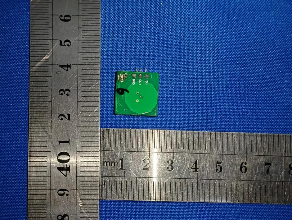
Click to zoom
Application Details
- Equipment Class
- DXX - Part 15 Low Power Communication Device Transmitter
- Date of Grant
- Jun 28, 2023
- Application Purpose
- Original Equipment
- Date of Application
- Jun 28, 2023
- Equipment Note
- 5.8GHz Microwave Motion sensor
- Frequency Range
- 5800.00000000 - 5800.00000000
- Company
- Fine Made Micro Co., Ltd.
- Country
- China
Documents & Files
Document Text
Text extracted from the exhibit documents filed with the FCC. Open a document above to read the original.
Users Manual
富满微电子集团股份有限公司 FINE MADE MICROELECTRONICS GROUP CO., LTD. FM5821-2020 User Guide 5.8GHz Microwave Motion sensor FM5821 User Guide Description FM5821-2020 is a miniaturized 5.8G radar sensor module made by FM, with a size of 20mm by 20mm. It is equipped with the FM5821 radar sensor chip, developed by FM, which integrates 5.8G RF microwave transmit and receive circuits and an IF amplifier circuit. The sensor also has a small, integrated antenna developed by FM, which makes it suitable for use in light fixture modules due to its small size and high performance. It is irreplaceable in detecting human movement and intelligent sensing scenarios and is therefore widely used in the smart home, Internet of Things, and intelligent lighting markets. Radar Sensor’s illustration 1 MCU AT5810 chip and microwave circuit LDO IN/OUTPUT IN/OUTPUT RX TX ANT LED 20mm 20mm Figure 1 FM5821-2020 Radar Sensor Input and Output Interface FM5821-2020 can be embedded in end product with three contact PINs, the PIN space is 2.54mm/2.00mm, below is the detail description about the interface Pin Name Function Note VCC Power supply LDO is not attached by default, VCC is 5V, the default power consumption of the module is 17mA GND Ground PIN s OUT Output control Output is 5V TTL by default, could be PWM if needed Specifications Parameters Min. Typical Max. Unit Note Frequency 5800MHz TX Power -6 dBm Input VCC 4.5 5 5.5 V Without external LDO Output High Level 5 V Output Low Level 0 V Current 17 18 mA Mounting Height 3 10 M Can be tuned if needed Detection Radius 5 10 M Related to mounting height Hold time 10 S Can be tuned if needed Daylight sensor 10 Lux Can be tuned if needed Operating TEMP -30 105 °C Radar signal processing The FM5820 radar sensor chip is mounted on the FM5821-2020. After completing the power-on operation, the MCU initializes the chip through the I2C interface, configuring parameters such as the transmission frequency and receiving gain. This allows the chip to collect and extract the intermediate frequency signal of the human body's motion through the antenna, and then the MCU acquires the intermediate frequency signal through the ADC, and outputs the GPIO signal according to the amplitude and frequency of the intermediate frequency signal. Detected distance The detection distance of the radar sensor module depends on the sensitivity of receiving mobile signals. This can be controlled by the MCU on the module. The maximum linear detection distance is 10m. The actual detection distance of the hoisting depends on the height of the hoisting and the angle of detection. In the case of extremely high sensitivity, self-excitation may occur, so the sensitivity needs to be configured according to the actual use requirements. The following figure is a schematic diagram of the detection range of the radar in the case of a straight line. The dark area is the high-sensitivity area. In this area It is easy to detect human movement in the interior, the lighter the color, the lower the receiving sensitivity Figure 2 FM5821-2020 Radar Sensor detection pattern Block Diagram & Description 5V LDO 3.3V MCU 3.3V 5821 SCL SDA IF TX RX 25M LED GPIO Figure 3 FM5821-2020 Radar Sensor Block Diagram The input 5V voltage is converted to a 3.3V voltage by the LDO, which powers both the MCU and the 5821. The 25M crystal oscillator provides a clock signal for the 5821 digital circuitry to function properly. The MCU configures the 5821's registers through the I2C protocol, and the 5821 receives sensing signals through its TX RX radio frequency channels, transmitted via the antenna. The output IF signal is then collected by the MCU's ADC module and, after being judged by the MCU, a GPIO signal is output to the LED. Installation Notes 1. Do not place any metal objects in front of the antenna. Thin plastic and glass are acceptable, but keep a gap of at least 2mm between the antenna and the cover. 2. When there are multiple radar sensors in the same space, position the antennas parallel to each other, with a minimum gap of 1m between the sensors. 3. Power frequency can interfere with radar signal, so keep the LED driver away from the antenna and do not place it directly in front of it. 4. The sensor has a power consumption of approximately 35mA. Ensure that the LED driver has a current-driving capability of at least 50mA. FCC WARNING FCC Caution: Any changes or modifications not expressly approved by the party responsible for compliance could void the user's authority to operate this equipment. This device complies with Part 15 of the FCC Rules. Operation is subject to the following two conditions: (1) This device may not cause harmful interference, and (2) this device must accept any interference received, including interference that may cause undesired operation. This device and its antenna(s) must not be co-located or operating in conjunction with any other antenna or transmitter. 15.105 Information to the user. (b) For a Class B digital device or peripheral, the instructions furnished the user shall include the following or similar statement, placed in a prominent location in the text of the manual: Note: This equipment has been tested and found to comply with the limits for a Class B digital device, pursuant to part 15 of the FCC Rules. These limits are designed to provide reasonable protection against harmful interference in a residential installation. This equipment generates, uses and can radiate radio frequency energy and, if not installed and used in accordance with the instructions, may cause harmful interference to radio communications. However, there is no guarantee that interference will not occur in a particular installation. If this equipment does cause harmful interference to radio or television reception, which can be determined by turning the equipment off and on, the user is encouraged to try to correct the interference by one or more of the following measures: —Reorient or relocate the receiving antenna. —Increase th…
Text truncated - open the document above for the full version.
Attestation Statements
(FineMadeMicroCo.,Ltd.) (Apr.27,2023) EurofinsElectricalandElectronicTestingNA,Inc. 914WestPatapscoAvenue Baltimore,MD21230 RE:AttestationStatementsPart2.911(d)(5)(i)requestfor(2BAY5FM5831-1919) [FineMadeMicroCo.,Ltd.](“theapplicant”)certifiesthattheequipmentforwhich authorizationissoughtisnot“covered”equipmentprohibitedfromreceivingan equipmentauthorizationpursuanttosection2.903oftheFCCrules. Sincerely, (Applicantsignature) (Applicantprintedname)ShaoChangGang (FineMadeMicroCo.,Ltd.) (Apr.27,2023) EurofinsElectricalandElectronicTestingNA,Inc. 914WestPatapscoAvenue Baltimore,MD21230 RE:AttestationStatementsPart2.911(d)(5)(ii)requestfor(2BAY5FM5831-1919) [FineMadeMicroCo.,Ltd.](“theapplicant”)certifiesthat,asofthedateofthefilingof theapplication,theapplicantisnotidentifiedontheCoveredListasanentityproducing “covered”equipment. Sincerely, (Applicantsignature) (Applicantprintedname) ShaoChangGang
Cover Letter(s)
< Fine Made Micro Co., Ltd.> Eurofins Electrical and Electronic Testing NA, Inc. 914 West Patapsco Avenue Baltimore, MD 21230 Company name: Fine Made Micro Co., Ltd. FCC ID: 2BAY5FM5831-1919 Gentlemen, In accordance with 47CFR 15.212 Modular Transmitters and KDB 996369 D01 ‘Module Certification Guide v02’. FCC ID: 2BAY5FM5831-1919 has been examined against the following requirements. Items to be covered by Single modular transmitters. Requirement per 15.212 and KDB 996369 D01 ‘Modular Certification Guide v02 Explanation from Grantee (do not write yes/no, but explain why product complies/how it is achieved) 1.The radio elements must have the radio frequency circuitry shielded. Physical components and tuning capacitor(s) may be located external to the shield, but must be on the module assembly The modular have the radio frequency circuitry shielded 2.The module must have buffered modulation/data inputs to ensure that the device will comply with Part 15 requirements with any type of input signal All modulation and data inputs are buffered by circuitry on the transmitter chip FM5821 as is shown in the schematic. 3.The module must contain power supply regulation on the module Power supply regulation is provided by circuitry on the transmitter chip FM5821, as is shown in the schematic. 4.The module must contain a permanently attached antenna, or contain a unique antenna connector, and be marketed and operated only with specific antenna(s), per Sections 15.203, 15.204(b), 15.204(c), 15.212(a), 2.929(b) EUT module contain a permanently attached antenna. Please reference the exhibition Test Report. 5.The module must demonstrate compliance in a stand- alone configuration Please reference exhibition Test Configuration Photo for the stand-alone test configuration. 6.The module must be labelled with its permanently affixed FCC ID label, or use an electronic display (See KDB Publication 784748 about labelling requirements) The instruction on the labelling rule of the end product has been stated in the Users manual of this module. Please also see the exhibition Label Sample. 7.The module must comply with all specific rules applicable to the transmitter including all the conditions provided in the integration instructions by the grantee The required FCC rule has been fulfilled and all the instructions for maintaining compliance has been clearly stated in the Users Manual. 8.The module must comply with RF exposure requirements Please refer exhibition RF Exposure for the compliance of MPE RF exposure rule. Name: Shao Chang Gang Title: Engineer Signature of applicant Date: 2023.05.09
Cover Letter(s)
Fine Made Micro Co., Ltd. (2023.05.09) Eurofins Electrical and Electronic Testing NA, Inc. 914 West Patapsco Avenue Baltimore, MD 21230 RE: CONFIDENTIALITY REQUEST FOR (5.8GHz Microwave Motion sensor / FM5831-1919 / FCC ID: 2BAY5FM5831-1919 ) To Whom It May Concern: This letter serves as an official request for confidentiality under sections 0.457 and 0.459 of CFR 47. We have requested that the Exhibits Long-Term Confidentiality Short-Term Confidentiality NOTE 2 ID Label/Location No No Attestation Statement No No External Photos No ☒ Block Diagram ☒ ☐ Schematics ☒ ☐ Test Report No No Test Setup Photos No ☒ User’s Manual ☐ NOTE 1 ☒ Internal Photos ☐ NOTE 1 ☒ Parts List / Tune Up ☐ ☐ RF Exposure Info No No Operational Description ☒ ☐ Cover Letter(s) No No SDR Software / Security Info ☐ No required to be submitted with this application be permanently withheld from public review. Above mentioned document contains detailed system and equipment description are considered as proprietary information in operation of the equipment. The public disclosure of above documents might be harmful to our company and would give competitor an unfair advantage in the market. Please contact me if there is any information you may need. Sincerely, Signature: Name: Shao Chang Gang Title: Engineer
Cover Letter(s)
Fine Made Micro Co., Ltd. (2023.05.09) Eurofins Electrical and Electronic Testing NA, Inc. 914 West Patapsco Avenue Baltimore, MD 21230 RE: LETTER OF AGENT AUTHORIZATION To Whom It May Concern: We, the undersigned, hereby authorize (Shenzhen CTB Testing Technology Co., Ltd.) to act on our behalf in all matters relating to application for equipment authorization, including the signing of all documents relating to these matters. We also hereby certify that no party to the application authorized hereunder is subject to the denial of benefits, including FCC benefits, pursuant to Section 5301 of the Anti-Drug Abuse Act of 1988, 21 U.S.C.853(a). This agreement expires one year from the current date. Sincerely, Signature: Name: Shao Chang Gang Title: Engineer
External Photos
External Photos ANT
ID Label/Location Info
FCC ID LABEL: Label Location: FCC ID: 2BAY5FM5831-1919
Internal Photos
Internal Photos
RF Exposure Info
FCC §15.247 (i), §2.1091 – RF Exposure FCC ID: 2BAY5FM5831-1919 Applied procedures / limit According to FCC §15.247(i) and §1.1307(b)(1), systems operating under the provisions of this section shall be operated in a manner that ensures that the public is not exposed to radio frequency energy level in excess of the Commission’s guidelines. Limits for Occupational / Controlled Exposure Frequency Range (MHz) Electric Field Strength (E) (V/m) Magnetic Field Strength (H) (A/m) Power Density (S) (mW/ cm 2 ) Averaging Time |E| 2 ,|H| 2 or S (minutes) 0.3-3.0 614 1.63 (100)* 6 3.0-30 1842 / f 4.89 / f (900 / f)* 6 30-300 61.4 0.163 1.0 6 300-1500 F/300 6 1500-100,000 5 6 Note: ƒ is frequency in MHz * = Power density limit is applicable at frequencies greater than 100 MHz Limits for General Population / Uncontrolled Exposure Frequency Range (MHz) Electric Field Strength (E) (V/m) Magnetic Field Strength (H) (A/m) Power Density (S) (mW/ cm 2 ) Averaging Time |E| 2 ,|H| 2 or S (minutes) 0.3-1.34 614 1.63 (100)* 30 1.34-30 824/f 2.19/f (180/f)* 30 30-300 27.5 0.073 0.2 30 300-1500 F/1500 30 1500-100,000 1.0 30 Note: f = frequency in MHz * = Plane-wave equivalent power density MPE PREDICTION Predication of MPE limit at a given distance, Equation from OET Bulletin 65, Edition 97-01 Where: S = power density P = power input to antenna G = power gain of the antenna in the direction of interest relative to an isotropic radiator R = distance to the center of radiation of the antenna,R=20cm Test Result of RF Exposure Evaluation Note:dbm=dbuv/m-95.2=83.79-95.2=-11.41dBm(EIRP), so the conduct peak power=-11.41- 4.87=-16.28dBm Modes& Channel Freq. (MHz) Tune up Produce power Maximu m peak output power (dBm) Output power to antenna (mW) Antenna Gain (numeric) Power Density (S) (mW/ cm2) Limit (mW / cm2 ) Result 5.8GHz 5800 -17±1 -16 0.0251 3.069 (4.87dBi) 0.000015 1 Pass
Test Report
Antenna manufacturer: Shanghai Yingsi Microelectronics Co., LTD. Antenna type: microstrip patch antenna Dimensions: Regular decagon with a radius of 6.69mm 增益: 频率:
Test Report
TEST REPORT Compiled by: Reviewed by: Approved by: Chen Zheng Arron Liu Bin Mei / Director Note: If there is any objection to the inspection results in this report, please submit a written report to the company within 15 days from the date of receiving the report. The test report is effective only with both signature and specialized stamp. This result(s) shown in this report refer only to the sample(s) tested. Without written approval of Shenzhen CTB Testing Technology Co., Ltd. this report can’t be reproduced except in full. The tested sample(s) and the sample information are provided by the client. “*” indicates the testing items were fulfilled by subcontracted lab. “#” indicates the items are not in CNAS accreditation scope. Product Name: 5.8GHz Microwave Motion sensor FCC ID: 2BAY5FM5831-1919 Trademark: N/A Model Number: FM5831-1919 Prepared For: Fine Made Micro Co., Ltd. Address: 11th Floor, Building A, Jindi Century Building, Qiaoxiang Road, Nanshan District, Shenzhen City, Guangdong Province Manufacturer: Fine Made Micro Co., Ltd. Address: 11th Floor, Building A, Jindi Century Building, Qiaoxiang Road, Nanshan District, Shenzhen City, Guangdong Province Prepared By: Shenzhen CTB Testing Technology Co., Ltd. Address: 1&2/F., Building A, No.26, Xinhe Road, Xinqiao, Xinqiao Street, Bao'an District, Shenzhen, Guangdong, China Sample Received Date: Feb. 15, 2023 Sample tested Date: Feb. 15, 2023 to Jun. 26, 2023 Issue Date: Jun. 26, 2023 Report No.: CTB230425027RFX Test Standards FCC Part15.249 ANSI C63.10:2013 Test Results PASS Remark: This is 2.4GHz radio test report. TABLE OF CONTENT Test Report Declaration Page 1. VERSION .......................................................................... 3 2. TEST SUMMARY ................................................................... 4 3. MEASUREMENT UNCERTAINTY ..................................................... 5 4. PRODUCT INFORMATION AND TEST SETUP .......................................... 6 4.1 Product Information .................................................................... 6 4.2 Test Setup Configuration ............................................................... 6 4.3 Support Equipment .................................................................... 6 4.4 Channel List .......................................................................... 7 4.5 Test Mode ............................................................................ 7 4.6 Test Environment ...................................................................... 7 5. TEST FACILITY AND TEST INSTRUMENT USED ....................................... 8 5.1 Test Facility ........................................................................... 8 5.2 Test Instrument Used .................................................................. 8 6. AC POWER LINE CONDUCTED EMISSION ............................................ 10 6.1 Block Diagram Of Test Setup .......................................................... 10 6.2 Limit ................................................................................ 10 6.3 Test procedure ....................................................................... 10 6.4 Test Result .......................................................................... 12 7. RADIATED SPURIOUS EMISSION ................................................... 14 7.1 Block Diagram Of Test Setup .......................................................... 14 7.2 Limit ................................................................................ 14 7.3 Test procedure ....................................................................... 15 7.4 Test Result .......................................................................... 16 8. BAND EDGE AND RF COUNDUCTED SPURIOUS EMISSIONS .......................... 19 8.1 Block Diagram Of Test Setup .......................................................... 19 8.2 Limit ................................................................................ 19 8.3 Test procedure ....................................................................... 20 8.4 Test Result .......................................................................... 21 9. BANDWIDTH TEST ................................................................ 23 9.1 Block Diagram Of Test Setup .......................................................... 23 9.2 Limit ................................................................................ 23 9.3 Test procedure ....................................................................... 23 9.4 Test Result .......................................................................... 23 10. ANTENNA REQUIREMENT ......................................................... 25 11. EUT TEST SETUP PHOTOGRAPHS .................................................. 27 (Note: N/A means not applicable) 1. VERSION Report No. Issue Date Description Approved CTB230425027RFX Jun. 26, 2023 Original Valid 2. TEST SUMMARY The Product has been tested according to the following specifications: Standard Section Test Item Judgment Remark 15.207 Conducted Emission PASS 15.215 20dB Bandwidth PASS 15.249 Fundamental &Radiated Spurious Emission Measurement PASS 15.205 Band Edge Emission PASS 15.203 Antenna Requirement PASS Remark: Test according to ANSI C63.10-2013. 3. MEASUREMENT UNCERTAINTY Where relevant, the following measurement uncertainty levels have been estimated for tests performed on the Product as specified in CISPR 16-4-2. This uncertainty represents an expanded uncertainty expressed at approximately the 95% confidence level using a coverage factor of k=2. Item Uncertainty Occupancy bandwidth 54.3kHz Conducted output power Above 1G 0.9dB Conducted output power below 1G 0.9dB Power Spectral Density , Conduction 0.9dB Conduction spurious emissions 2.0dB Out of band emission 2.0dB 3m camber Radiated spurious emission(9KHz-30MHz) 4.8dB 3m camber Radiated spurious emission(30MHz-1GHz) 4.6dB 3m chamber Radiated spurious emi…
Text truncated - open the document above for the full version.
Test Setup Photos
Radiated Emission Below 1G Above 1G Conducted emissions
Contact Information
Applicant
Shao Chang Gang
Test Firm
Shenzhen CTB Testing Technology Co., Ltd.Rita Xiao
[email protected]86-13538218145
Technical Specifications
| # | Rule Parts | Frequency Range | Power Output |
|---|---|---|---|
| 1 | 15C | 5.80 GHz - 5.80 GHz | - |