2BBZMLECOO-C8Smart sunglasses
Shenzhen Yuan Xin Chuang Zhan Supply Chain Co.,Ltd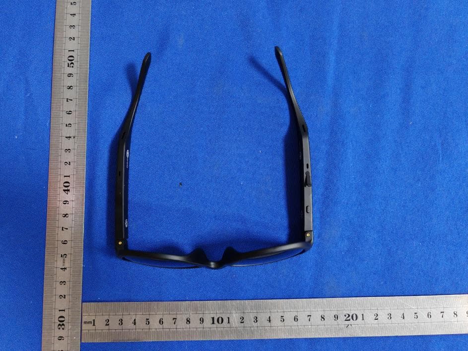
Click to zoom
Application Details
- Equipment Class
- DSS - Part 15 Spread Spectrum Transmitter
- Date of Grant
- Jul 16, 2023
- Application Purpose
- Original Equipment
- Date of Application
- Jul 16, 2023
- Equipment Note
- Smart sunglasses
- Frequency Range
- 2402.00000000 - 2480.00000000
- Country
- China
Documents & Files
Document Text
Text extracted from the exhibit documents filed with the FCC. Open a document above to read the original.
Users Manual
真无线蓝牙眼镜 C8 说明书 开关机及蓝牙配对 操作说明 Instructions 长按2秒MFB键开/关机,开机时蓝色LED闪烁,语 音提示“power on”;关机时红色LED闪烁,语音 提示“power off” 开关机 标准配置 产品外观 Smart Glasses x1 单击触控区域为音量+,调节到最大音量时有提示声 音量设置 长按触控区域为音量- 语音助手/Siri:双击MFB键 接听电话:单击MFB键 拒接电话:单击触控区域 挂断电话:单击MFB键 调用语音助手 通话设置 充电时间约1.5小时,低电报警语音提示 “battery low” 低电报警间隔60秒,红灯闪烁,充电时红色LED灯 亮,充满后蓝色LED灯亮 充电过程中不能开机 开机后进入配对模式,打开需连接设备蓝牙,搜索 Lecoo-C8进行配对,配对成功后(语音提示“联 机成功”)蓝灯3秒闪一次,断开蓝牙连接,重新 进入配对模式。 配对模式 开机后自动回连最后连接过的蓝牙设备,5分钟无蓝 牙连接自动关机。 1 音频模式 2 充电模式 Power on/off & Bluetooth pairing Warning message Long press the MFB button for 2 seconds to turn on/o , the blue LED ashes when turning on, and the voice prompt “power on” ,the red light ashes when turning o , and the voice prompt “power o ” Power on/o 3 保修说明 Power on ,enter the pairing mode,and turn on the Bluetooth of the device to be connected, search for “Lecoo-C8” for pairing, and the blue light will ash per 3 seconds after the pairing is successful. (voice prompt “Lian ji cheng gong”) It will automatically enter the pairing mode after disconnecting Automatically connect back to the last connected Bluetooth device after power on, Automatic shutdown without Bluetooth connection in 5 minutes One click the touch area to be volume +, there will be a prompt sound when the volume is adjusted to the maximum Long press the touch area for volume - One click the MFB button to answer phone call One click the touch area to reject phone call One click the MFB button to hang up the current call Double-click the MFB button Charging time about 1.5 hours, low battery alarm voice prompt “battery low” Unable turning on while charging Low battery alarm interval is 60 seconds, red light ashes, The red LED is on when charging, and the blue LED is on when it is full Bluetooth pairing 1 Audio mode Volume setting 2 Call mode Voice assistant Charging mode 3 Standard con guration Appearance 触控区域 出声孔 USB充电孔 MFB键 TAC偏光镜片 Touch area Speaker Charging port MFB TAC Polarized lenses Charging Cable x1 性别年龄用户姓名 来酷产品保修卡 联系电话 邮政编码 电子邮箱 联系地址 销售日期 产品序列号 销售单位名称 销售发票号码 非维修范围 眼镜x1USB充电线x1 眼镜布x1 Glasses cloth x1 就本文件附随的产品做如下保证:如产品在您购买日 起十二(12)个月(“保修期”)内,在正常使用情 况下因质量瑕疵发生损坏,免费修理;维修后的产品, 在剩余保修期内继续享有保修。购买日以销售发票日 期为准;如无法确定购买日,则保修期自产品生产日 期起按十三(13)个月计算。 1.涂改保修卡、产品编码与产品本体 不符; 2.因误用、滥用或不适当的运输、使 用、维护或保管而导致的故障或损 坏; 3.因不可抗力(如地震、战争、火灾 等)或意外导致的故障或损坏; 4.任何因尖锐物体造成的损坏 5.有烧损或水浸迹象的产品 6.因擅自拆改导致的损坏 7.产品正常使用过程中发生的老化、 脱色、磨损、破裂和其他损耗 4 想要更详细的了解真无线蓝牙眼镜请登录 服务监督热线:400-0100-800 邮箱 : [email protected] This device complies with part 15 of the FCC Rules. Operation is subject to the following two conditions: (1) this device may not cause harmful interference, and (2) this device must accept any interference received, including interference that may cause undesired operation. Any changes or modi cations not expressly approved by the party responsible for compliance could void the user's authority to operate the equipment. NOTE: This equipment has been tested and found to comply with the limits for a Class B digital device, pursuant to Part 15 of the FCC Rules. These limits are designed to provide reasonable protection against harmful interference in a residential installation. This equipment generates, uses and can radiate radio frequency energy and, if not installed and used in accordance with the instructions, may cause harmful interference to radio communications. However, there is no guarantee that interference will not occur in a particular installation. If this equipment does cause harmful interference to radio or television reception, which can be determined by turning the equipment o and on, the user is encouraged to try to correct the interference by one or more of the following measures: -- Reorient or relocate the receiving antenna. -- Increase the separation between the equipment and receiver. -- Connect the equipment into an outlet on a circuit di erent from that to which the receiver is connected. -- Consult the dealer or an experienced radio/TV technician for help. The device has been evaluated to meet general RF exposure requirement. The device can be u sed in portable exposure condition without restriction.
Attestation Statements
(Shenzhen Yuan Xin Chuang Zhan Supply Chain Co.,Ltd) (July 12, 2023) Eurofins Electrical and Electronic Testing NA, Inc. 914 West Patapsco Avenue Baltimore, MD 21230 RE: Attestation Statements Part 2.911(d)(5)(i) request for (FCC ID:2BBZMLECOO-C8) [Shenzhen Yuan Xin Chuang Zhan Supply Chain Co.,Ltd] (“the applicant”) certifies that the equipment for which authorization is sought is not “covered” equipment prohibited from receiving an equipment authorization pursuant to section 2.903 of the FCC rules. Sincerely, (Applicant signature) (Applicant printed name) Rong Zhang (Shenzhen Yuan Xin Chuang Zhan Supply Chain Co.,Ltd) (July 12, 2023) Eurofins Electrical and Electronic Testing NA, Inc. 914 West Patapsco Avenue Baltimore, MD 21230 RE: Attestation Statements Part 2.911(d)(5)(ii) request for (FCC ID:2BBZMLECOO-C8) [Shenzhen Yuan Xin Chuang Zhan Supply Chain Co.,Ltd] (“the applicant”) certifies that, as of the date of the filing of the application, the applicant is not identified on the Covered List as an entity producing “covered” equipment. Sincerely, (Applicant signature) (Applicant printed name) Rong Zhang
Cover Letter(s)
Shenzhen Yuan Xin Chuang Zhan Supply Chain Co.,Ltd (2023.07.10) Eurofins Electrical and Electronic Testing NA, Inc. 914 West Patapsco Avenue Baltimore, MD 21230 RE: CONFIDENTIALITY REQUEST FOR (Smart sunglasses / LECOO-C8 / FCC ID: 2BBZMLECOO-C8) To Whom It May Concern: This letter serves as an official request for confidentiality under sections 0.457 and 0.459 of CFR 47. We have requested that the Exhibits Long-Term Confidentiality Short-Term Confidentiality NOTE 2 ID Label/Location No No Attestation Statement No No External Photos No ☐ Block Diagram ☒ ☐ Schematics ☒ ☐ Test Report No No Test Setup Photos No ☐ User’s Manual ☐ NOTE 1 ☒ Internal Photos ☐ NOTE 1 ☒ Parts List / Tune Up ☐ ☐ RF Exposure Info No No Operational Description ☒ ☐ Cover Letter(s) No No SDR Software / Security Info ☐ No required to be submitted with this application be permanently withheld from public review. Above mentioned document contains detailed system and equipment description are considered as proprietary information in operation of the equipment. The public disclosure of above documents might be harmful to our company and would give competitor an unfair advantage in the market. Please contact me if there is any information you may need. Sincerely, Signature: Name: Rong Zhang Title: project manager
Cover Letter(s)
Shenzhen Yuan Xin Chuang Zhan Supply Chain Co.,Ltd (2023.07.10) Eurofins Electrical and Electronic Testing NA, Inc. 914 West Patapsco Avenue Baltimore, MD 21230 RE: LETTER OF AGENT AUTHORIZATION To Whom It May Concern: We, the undersigned, hereby authorize (Shenzhen CTB Testing Technology Co., Ltd.) to act on our behalf in all matters relating to application for equipment authorization, including the signing of all documents relating to these matters. We also hereby certify that no party to the application authorized hereunder is subject to the denial of benefits, including FCC benefits, pursuant to Section 5301 of the Anti-Drug Abuse Act of 1988, 21 U.S.C.853(a). This agreement expires one year from the current date. Sincerely, Signature: Name: Rong Zhang Title: project manager
External Photos
External Photos
ID Label/Location Info
FCC ID LABEL: Label Location: FCC ID: 2BBZMLECOO-C8 Model No.: LECOO-C8
Internal Photos
Internal Photos ANT
RF Exposure Info
Shenzhen CTB Testing Co., Ltd. FCC ID: 2BBZMLECOO-C8 Portable device According to §15.247(e)(i) and §1.1307(b)(1), systems operating under the provisions of this section shall be operated in a manner that ensures that the public is not exposed to radio frequency energy level in excess of the Commission’s guidelines. According to KDB447498 D01 General RF Exposure Guidance V06 The 1-g SAR and 10-g SAR test exclusion thresholds for 100 MHz to 6 GHz at test separation distances ≤ 50 mm are determined by: [(max. power of channel, including tune-up tolerance, mW)/(min. test separation distance, mm)]·[√f(GHZ)] ≤ 3.0 for 1-g SAR and ≤ 7.5 for 10-g extremity SAR, where: • f(GHZ) is the RF channel transmit frequency in GHz • Power and distance are rounded to the nearest mW and mm before calculation • The result is rounded to one decimal place for comparison When the minimum test separation distance is < 5 mm, a distance of 5 mm is applied to determine SAR test exclusion. EDR: Modulation Channel Freq. (GHz) Conduct ed power (dBm) Conducte d power (mW) Tune-up power (dBm) Max tune-up power (dBm) Max tune-up power (mW) Distance (mm) Result calculatio n SAR Exclusion threshold SAR test exclusion 2.402 -0.544 0.88 0±1 1.00 1.26 <5 0.39023 3.00 YES 2.441 -0.734 0.84 0±1 1.00 1.26 <5 0.39338 3.00 YES 2.480 -0.143 0.97 0±1 1.00 1.26 <5 0.39651 3.00 YES 2.402 0.247 1.06 0±1 1.00 1.26 <5 0.39023 3.00 YES 2.441 0.097 1.02 0±1 1.00 1.26 <5 0.39338 3.00 YES 2.480 0.671 1.17 0±1 1.00 1.26 <5 0.39651 3.00 YES 2.402 0.604 1.15 0±1 1.00 1.26 <5 0.39023 3.00 YES 2.441 0.515 1.13 0±1 1.00 1.26 <5 0.39338 3.00 YES 2.480 1.075 1.28 1±1 2.00 1.58 <5 0.49918 3.00 YES GFSK π /4DQPSK 8DQPSK Conclusion: For the max result : 0.49918≤ FCC Limit 3.0 for 1g SAR.
Test Report
Sunlord Specifications for Chip AntennaPage 1 of 8 Preliminary [New Released,Revised]SPEC No.: ES010-01 Shenzhen Sunlord Electronics Co., Ltd. 【 For Customer approval Only 】 Date: Qualification Status:FullRestrictedRejected Approved ByVerified ByRe-checked ByChecked By Comments: Customer Product Name Chip Antenna Sunlord Part Number SLDA31-2R400G-S2TF Customer Part Number Approved By Checked ByIssued By 【 This SPEC is total 8 pages including specifications and appendix. 】 【 ROHS Compliant Parts 】 Address: Sunlord Industrial Park, Dafuyuan Industrial Zone, Baoan, Shenzhen, China 518110 Tel: 0086-755-29832660 Fax: 0086-755-82269029 E-Mail: [email protected] SPECIFICATIONS Sunlord Specifications for Chip AntennaPage 2 of 8 【 Version change history 】 Rev.Effective DateChanged ContentsChange reasonsApproved By 01Nov.15,2017New Release/Hai Guo Sunlord Specifications for Chip AntennaPage 3 of 8 1. Scope This specification applies to SLDA31-2R400G-S2TF of Multi-layer Chip Antenna. 2. Product Description and Identification (Part Number) 1) Description :Multi-layer Chip Antenna 2) Product Identification (Part Number) SLDA31-2R400G-S2TF ① ② ③④ ⑤ ⑥ 3. Electrical Characteristics Part Number Band WidthPeak GainAverage GainVSWRImpedance Power Capacity MHz 2.5 dBi @( XZ-total) 0.5 dBi @( XZ-total) In BWΩW SLDA31-2R400G-S2TF≥100< 2502 W max 1) Operating and storage temperature range (individual chip without packing): -40 °C ~ +85 °C . 2) Storage temperature range (packaging conditions): -10 °C ~ +40 °C and RH 70% (Max.). 3) Test equipment: Network Analyzer: E5071C. 4) Measuring diagram. 4. Shape and Dimensions Dimensions and recommended PCB pattern for reflow soldering: A B D C (1) (2) Unit: mm Item ABCD. SLDA31 3.2±0.2 1.6±0.2 0.5±0.1 0.5±0.2 ① Type SLDAMultilayer Chip Antenna ④ Series Code S2 ② External Dimensions (L×W) (mm) 313.2×1.6 ③ Center Frequency 2R400G2400.0MHz ⑤ Packing TTape Carrier Package 6 Hazardous Substance Free Products F Sunlord Specifications for Chip AntennaPage 4 of 8 Demo-board: Topview Detailview Bottomview 1) Terminal Configuration: 5. Test and Measurement Procedures 5.1 Test Conditions No.Terminal NameNo.Terminal Name (1)Feeding Point(2)Soldering terminal (2)(1) 50Ω trace GND via Unit: mm Sunlord Specifications for Chip AntennaPage 5 of 8 Unless otherwise specified, the standard atmospheric conditions for measurement/test as: a. Ambient Temperature: 20±15 °C b. Relative Humidity: 65±20% c. Air Pressure: 86 Pa to 106KPa If any doubt on the results, measurements/tests should be made within the following limits: a. Ambient Temperature: 20±2 °C b. Relative Humidity: 65±5% c. Air Pressure: 86KPa to 106KPa 5.2 Visual Examination a. Inspection Equipment: 20 X magnifier 5.3 Reliability Test ItemsRequirementsTest Methods and Remarks 5.3.1 Terminal Strength No visible mechanical damage. 1 Solder the Antenna to the testing jig (glass epoxy board shown as the following figure) using leadfree solder. Then apply a force in the direction of the arrow. 2 10N force for 3216 series. 3 Keep time: 10±1sec. 5.3.2 Resistance to Flexure No visible mechanical damage. 1 Solder the chip to the test jig (glass epoxy board) using a leadfree solder. Then apply a force in the direction shown as the following figure. Solder the chip to the test jig (glass epoxy board) using leadfree solder. Then apply a force in the direction. 2 Flexure: 2mm 3 Pressurizing Speed: 0.5mm/sec 4 Keep time: ≥30 sec 5.3.3 Dropping No visible mechanical damage. SLDA series: Drop the chip 5 times on a wood floor from a height of 50 cm. 5.3.4 Solderability 1 No visible mechanical damage. 2 Wetting shall be exceeded 75% coverage. 1 Solder temperature: 240±2 °C 2 Duration: 3sec 3 Solder: Sn/3.0Ag/0.5Cu 4 Flux: 25% Resin and 75% ethanol in weight 5.3.5 Resistance to Soldering Heat No visible mechanical damage. 1 Solder temperature: 260±5 °C 2 Duration: 5 sec 3 Solder: Sn/3.0Ag/0.5Cu 4 Flux: 25% Resin and 75% ethanol in weight 5 The chip shall be stabilized at normal condition for 1~2 hours before measuring. 5.3.6 Thermal Shock 1 No visible mechanical damage. 2 Satisfy electrical Characteristic. 1 Temperature and time: -40 °C for 30±3 min→85 °C for 30±3min 2 Transforming interval: Max. 20 sec. 3 Tested cycle: 10 cycles 4 The chip shall be stabilized at normal condition for 1~2 hours before measuring. 20 45 45 R10 Flexure:2 10 Unit: mm 10N/10±1s Speed: 1.0mm/s Glass Epoxy Board Chip Mounting Pad Sunlord Specifications for Chip AntennaPage 6 of 8 5.3.7 Damp Heat (Steady States) 1 No visible mechanical damage. 2 Satisfy electrical Characteristic. 1 Temperature: 60±2 °C 2 Humidity: 90% to 95% RH 3 Duration: 96 +24 hours 4 The chip shall be stabilized at normal condition for 1~2 hours before measuring. 5.3.8 Resistance to High temperature 1 No visible mechanical damage. 2 Satisfy electrical Characteristic. 1 Temperature: 85±2 °C 2 Duration: 96 +24 hours 3 The chip shall be stabilized at normal condition for 1~2 hours before measuring. 6. Packaging and Storage 6.1 Packaging There is one type of packaging for the Multi-layer Chip Antennas. Please specify the packing code when ordering. 6.1.1 Tape Carrier Packaging: Packaging code: T a. Tape carrier packaging are specified in attached figureFig. 6.1-1~3 b. Tape carrier packaging quantity please see the following table: (1) Taping Drawings (Unit: mm) (2) Taping Dimensions (Unit: mm) Type3216[1206] TapePaper Tape Quantity3K -40 °C Ambient Temperature 85 °C 30 min. 30 min. 30 min. 20sec. (max.) Remark:The sprocket holes are to the right as the tape is pulled toward the user. Fig. 6.1-1 Sprocket Hole Chip Cavity Bottom Tape Paper Tape TopTape Paper Tape 1.75±0.1 4.0±0.1 A B P 3.5±0.058.0 ± 0.3 Chip Cavity SprocketHole Φ1.5 (+0.1,0) DirectionofFeed T 2.0±0.05 Sunlord Specifications for Chip AntennaPage 7 of 8 (3)Reel Dimensions (Unit: mm) 6.2 Storage a. The solderability of the external electrode may be deteriorated if packages are stored where they are exposed to high humidity. Package must be s…
Text truncated - open the document above for the full version.
Test Report
Shenzhen CTB Testing Technology Co., Ltd. Report No.:CTB230628030RFX Report Tel: 4008-707-283 Web: http://www.ctb-lab.net Page 1 of 58 TEST REPORT Compiled by: Reviewed by: Approved by: Chen Zheng Arron Liu Bin Mei / Director Note: If there is any objection to the inspection results in this report, please submit a written report to the company within 15 days from the date of receiving the report. The test report is effective only with both signature and specialized stamp. This result(s) shown in this report refer only to the sample(s) tested. Without written approval of Shenzhen CTB Testing Technology Co., Ltd. this report can’t be reproduced except in full. The tested sample(s) and the sample information are provided by the client. “*” indicates the testing items were fulfilled by subcontracted lab. “#” indicates the items are not in CNAS accreditation scope. Product Name: Smart sunglasses FCC ID: 2BBZMLECOO-C8 Trademark: LECOO Model Number: LECOO-C8 Prepared For: Shenzhen Yuan Xin Chuang Zhan Supply Chain Co.,Ltd Address: RM702, Building A of Rongchuangzhihui, Block of Road longsheng&Jinglong construction, Shangfen community, Mingzhi street, Longhua district, Shenzhen City. Manufacturer: Shenzhen Gonbes Technology Co.,Ltd Address: RM201, Building E, NO.9, Shangxue Industrial Part, Longgang District, Shenzhen City Prepared By: Shenzhen CTB Testing Technology Co., Ltd. Address: 1&2/F., Building A, No.26, Xinhe Road, Xinqiao, Xinqiao Street, Bao'an District, Shenzhen, Guangdong, China Sample Received Date: Jun. 25, 2023 Sample tested Date: Jun. 25, 2023 to Jun. 28, 2023 Issue Date: Jun. 28, 2023 Report No.: CTB230628030RFX Test Standards FCC Part15.247 ANSI C63.10:2013 Test Results PASS Remark: This is Bluetooth radio test report. Shenzhen CTB Testing Technology Co., Ltd. Report No.:CTB230628030RFX Report Tel: 4008-707-283 Web: http://www.ctb-lab.net Page 2 of 58 TABLE OF CONTENT Test Report Declaration Page 1. VERSION .......................................................................... 4 2. TEST SUMMARY ................................................................... 5 3. MEASUREMENT UNCERTAINTY ..................................................... 6 4. PRODUCT INFORMATION AND TEST SETUP .......................................... 7 4.1 Product Information .................................................................... 7 4.2 Test Setup Configuration ............................................................... 7 4.3 Support Equipment .................................................................... 7 4.4 Channel List .......................................................................... 8 4.5 Test Mode ............................................................................ 8 4.6 Test Environment ...................................................................... 8 5. TEST FACILITY AND TEST INSTRUMENT USED ....................................... 9 5.1 Test Facility ........................................................................... 9 5.2 Test Instrument Used .................................................................. 9 6. AC POWER LINE CONDUCTED EMISSION ............................................ 11 6.1 Block Diagram Of Test Setup .......................................................... 11 6.2 Limit ................................................................................ 11 6.3 Test procedure ....................................................................... 11 6.4 Test Result .......................................................................... 13 7. RADIATED SPURIOUS EMISSION ................................................... 15 7.1 Block Diagram Of Test Setup .......................................................... 15 7.2 Limit ................................................................................ 15 7.3 Test procedure ....................................................................... 16 7.4 Test Result .......................................................................... 17 8. BAND EDGE AND RF COUNDUCTED SPURIOUS EMISSIONS .......................... 26 8.1 Block Diagram Of Test Setup .......................................................... 26 8.2 Limit ................................................................................ 26 8.3 Test procedure ....................................................................... 26 8.4 Test Result .......................................................................... 27 9. COUDUCTED PEAK OUTPUT POWER ............................................... 34 9.1 Block Diagram Of Test Setup .......................................................... 34 9.2 Limit ................................................................................ 34 9.3 Test procedure ....................................................................... 34 9.4 Test Result .......................................................................... 35 10. 20DB OCCUPIED BANDWIDTH...................................................... 39 10.1 Block Diagram Of Test Setup ......................................................... 39 10.2 Limit ............................................................................... 39 10.3 Test procedure ...................................................................... 39 10.4 Test Result ......................................................................... 39 11. CARRIERFREQUENCIES SEPARATION .............................................. 43 11.1 Block Diagram Of Test Setup ......................................................... 43 11.2 Limit ............................................................................... 43 11.3 Test procedure ...................................................................... 43 11.4 Test Result ......................................................................... 43 12. HOPPING CHANNEL NUMBER ...................................................... 47 12.1 Block Diagram Of Test Setup .......…
Text truncated - open the document above for the full version.
Test Setup Photos
Radiated Emission Below 1G Above 1G Conducted emissions
Contact Information
Applicant
Rong Zhang
Test Firm
Shenzhen CTB Testing Technology Co., Ltd.Rita Xiao
[email protected]86-13538218145
Technical Specifications
| # | Rule Parts | Frequency Range | Power Output |
|---|---|---|---|
| 1 | 15C | 2.40 GHz - 2.48 GHz | 1.28 mW |