2BC43-IPISS202310Smart Diaper Cover
MEMSChip Co., Ltd.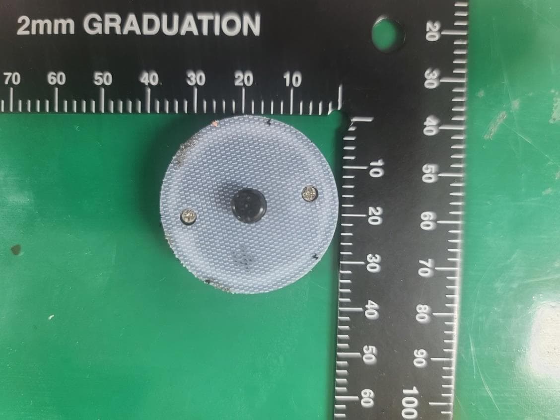
Click to zoom
Application Details
- Equipment Class
- DTS - Digital Transmission System
- Date of Grant
- Oct 30, 2023
- Application Purpose
- Original Equipment
- Date of Application
- Oct 30, 2023
- Equipment Note
- Smart Diaper Cover
- Frequency Range
- 2402.00000000 - 2480.00000000
- Company
- MEMSChip Co., Ltd.
- Country
- South Korea
Documents & Files
Document Text
Text extracted from the exhibit documents filed with the FCC. Open a document above to read the original.
Users Manual
T Model : IPISS Instruction Manual MEMSChip Co., Ltd. MEMS Sensor Leader 112 KETI, 25, Senari-ro, Bundang-gu Seongnum-Si, Gyeonggi-Do, KOREA, 13509 E-mail :[email protected] www.memschip.kr TEL : +80-70-4146-6259, Fax : +82-31-703-6259 Serial Bluetooth Terminal Setting l Serial Bluetooth Terminal is available for download in the Google Play store online. 1. Install Serial Bluetooth Terminal at smart phone. 2. Run the program (Serial bluetooth terminal) 3. Power on temperature-humidity module (power switch button) 4. Push the left icon(1) and then push the Devices button(2) % Execute Bluetooth pairing 5. Push the Scan button(3), Scanning ....(4) 6. Select FUS-****(device model name) and run the Edit button(5) 7. Select Custom mode and set like the picture First : 331a36f5-2459-45ea-9d956142foc4b307 Second : a73e9a10-628f-4494-a099-12efaf72258f Third : a9da6040-0823-4995-94ec-9ce41ca28833 8. Push the (√) icon, and then select the model name(FUS-****) Temperature and humidity values are displayed on the screen of smart phone English This device complies with Part 15 of the FCC Rules/Innovation Science and Economic Development Canada's licence-exempt RSS standard(s). Operation is subject to the following two conditions: (1) this device may not cause harmful interference, and (2) this device must accept any interference received, including interference that may cause undesired operation of the device. WARNING: Any changes or modifications to this unit not expressly approved by the party responsible for compliance could void the user’s authority to operate the equipment. This equipment has been tested and found to comply with the limits for a Class B digital device, pursuant to part 15 of the FCC Rules. These limits are designed to provide reasonable protection against harmful interference in a residential installation. This equipment generates, uses and can radiate radio frequency energy and, if not installed and used in accordance with the instructions, may cause harmful interference to radio communications. However, there is no guarantee that interference will not occur in a particular installation. If this equipment does cause harmful interference to radio or television reception, which can be determined by turning the equipment off and on, the user is encouraged to try to correct the interference by one or more of the following measures: • Reorient or relocate the receiving antenna. • Increase the separation between the equipment and receiver. • Connect the equipment into an outlet on a circuit different from that to which the receiver is connected. • Consult the dealer or an experienced radio/TV technician for help. FCCPart15.105statement
Attestation Statements
Rev 1/26/2023 MEMSChip Co., Ltd. BIZ-403, SKn Technopark 124, Saglmakgol-ro, Jungwon-gu, Seongnam-si, Gyeonggi-do, 13207, Republic of KOREA Federal Communications Commission Authorization and Evaluation Division 7435 Oakland Mills Road Columbia, MD 21046 USA Date: 2023-10-24 Ref: Attestation Statements Part 2.911(d)(5)(i) Filing FCC ID: 2BC43-IPISS202310 MEMSChip Co., Ltd. (“the applicant”) certifies that the equipment for which authorization is sought is not “covered” equipment prohibited from receiving an equipment authorization pursuant to section 2.903 of the FCC rules. Sincerely, YOUNG MIN KIM / CEO MEMSChip Co., Ltd. Rev 1/26/2023 MEMSChip Co., Ltd. BIZ-403, SKn Technopark 124, Saglmakgol-ro, Jungwon-gu, Seongnam-si, Gyeonggi-do, 13207, Republic of KOREA Federal Communications Commission Authorization and Evaluation Division 7435 Oakland Mills Road Columbia, MD 21046 USA Date: 2023-10-24 Ref: Attestation Statements Part 2.911(d)(5)(ii) Filing FCC ID: 2BC43-IPISS202310 MEMSChip Co., Ltd. (“the applicant”) certifies that, as of the date of the filing of the application, the applicant is not identified on the Covered List (as a specifically named entity or any of its subsidiaries or affiliates) as an entity producing “covered” equipment. Sincerely, YOUNG MIN KIM / CEO MEMSChip Co., Ltd.
Attestation Statements
Certification designating a U.S. Agent for service of process: As required by section 2.911(d)(7), the applicant must designate a contact located in the United States for purposes of acting as the applicant’s agent for service of process, regardless of whether the applicant is a domestic or foreign entity. An applicant located in the United States may designate itself as the agent for service of process. In either scenario, the designation of the U.S. agent for service of process should be provided as an attachment to the equipment authorization application. The applicant must provide a written certification, which must: i. Be signed by both the applicant and designated agent for service of process, if the agent is different from the applicant. ii. Acknowledge the applicant’s consent and the designated agent’s obligation to accept service of process. iii. Provide a physical U.S. address and email for the designated agent. iv. Acknowledge the applicant’s acceptance to maintain an agent for no less than one year after the grantee has terminated all marketing and importation or the conclusion of any Commission-related proceeding involving the equipment. Unofficial information provided by FCC personnel on February 14, 2023, via the monthly call with the TCB Council: The Agent for Process of Service: • cannot be a TCB or affiliated with a TCB (e.g. could not be a person who works for a TCB or a company that owns or is owned by the TCB) • cannot be a [FCC recognised] Lab or affiliated with a test lab (e.g. could not be a person who works for a Lab or a company that owns or is owned by the Lab) • Agent can be Individual Entity or a Company Entity • Agent Entity must be located in US, US address/phone • Entity acting as Agent must have FRN (best practice, put FRN on Agent Letter) • Agent letter does not have to be FCC ID specific, can be general Agent for Grantee For devices being marketed or for which marketing has ceased for less than 1 year, if the Agent for Process of Service changes, then for every TC Number the TCB must request the FCC to put application into Audit Mode and Agent Letter needs to be updated (superseded). NOTE: The U.S. Agent for Service of Process should not be confused with the authorized agent used for signing the 731 form, other cover letters within the application, and/or the agent who may interface with the TCB. MEMSChip Co., Ltd. U.S. Agent Designation for Service of Process ATTENTION: Federal Communications Commission Authorization and Evaluation Division 7435 Oakland Mills Road Columbia, MD 21046 USA REGARDING: FCC Certification – Section 2.911(d)(7) Information Designated U.S. Agent Company Name: Approve-IT, Inc. Contact Name: Nathan Grinager Street Address: 8011 34 th Ave South, Suite 342 City/Province/Zip: Bloomington, MN 55425 Telephone No: 651-247-1678 Email: [email protected] FRN #: 0027533835 This letter is to confirm that we (“the Designated U.S. Agent) have accepted the responsibility to act as the Designated U.S. Agent for Service of Process as required by section 47 CFR 2.911(d)(7) on behalf of the Applicant noted below. U.S. Agent Signature: Date: October 19, 2023 Signed by (Printed Name/Title): Nathan Grinager / Co-President *This letter is valid indefinitely for all applications submitted within the period of 10/19/2023 – 10/18/2024 The Applicant confirms its explicit consent and acknowledges that they must maintain an agent for no less than one year after terminating all marketing and importation OR the conclusion of any Commission-related proceeding involving the equipment. The applicant further acknowledges their responsibility to inform the FCC whenever the Designated U.S. Agent information above changes. Applicant Company name: MEMSChip Co., Ltd. Grantee FRN: 0034336750 FCC ID: 2BC43-IPISS202310 Contact Name: YOUNG MIN KIM Street Address: BIZ-403, SKn Technopark 124, Saglmakgol-ro City/Province/Zip: Jungwon-gu, Seongnam-si, Gyeonggi-do, 13207, Republic of KOREA Telephone No:+82-10-2690-6259 Email: [email protected] MEMSChip Co., Ltd. Applicant Signature: Date: 19/10/2023 Signed by (Printed Name/Title): YOUNG MIN KIM / CEO
Cover Letter(s)
RE: New Family Listing Declaration Model Name Differences Tested V Sincerely, MEMSChipCo.,Ltd. Date: Oct 19, 2023 Office of Engineering Technology Federal Communications Commission 7435 Oakland Mills Road Columbia, MD 21046 BIZ-403,SKnTechnopark124,Saglmakgol-ro,Jungwon-gu,Seongnam-si,Gyeonggi-do,13207,Republicof KOREA IPISSBasic model (Color: White or Black) For marketingmanagement (Color: White or Black) Temperature-HumidityModule Tmeperature-Humidity MeasurementDevice Please review the attached exhibits supporting our request for applying New Family Listing to the FCC ID:2BC43-IPISS202310for Company Name: MEMSChipCo., Ltd. Product Description: SmartDiaperSensor Base model: IPISS Additional model(s): Refer to the Following table The only difference between the base model IPISS and the additional model(s) are as follows: YOUNGMIN KIM/ CEO MEMSChipCo., Ltd.
Cover Letter(s)
PERMANENT Exhibit Type File Name PCBLayout Schematics Block diagram Operation description Andtheabovematerialscontaintradesecrets andproprietary informationnot customarily released tothepublic.The publicdisclosure ofthese materials may beharmfultothe applicant andprovideunjustifiedbenefits to its competitors. Theapplicant understands that pursuant toSection0.457oftheRules, disclosureofthis application andall accompanying documentation willnotbemade before the date ofthe Grant forthis application. Sincerely, Pursuant toSections0.457and0.459oftheCommission’sRules, weherebyrequest confidential treatment ofinformation accompanying this application asoutlinedbelow: Partlist Partlist.pdf MEMSChipCo., Ltd. BIZ-403,SKn Technopark124, Saglmakgol-ro,Jungwon-gu,Seongnam-si,Gyeonggi-do,13207,Republicof KOREA Date: Oct. 19, 2023 FederalCommunications Commission Authorization and Evaluation Division ConfidentialityRequest regarding application for certification ofFCC ID: 2BC43-IPISS202310 Bom.pdf Schemiatics.pdf BlockDiagram.pdf Operationdescription.pdf MEMSChipCo.,Ltd. YOUNGMIN KIM / CEO
Cover Letter(s)
MEMSChip Co., Ltd. BIZ-403, SKn Technopark 124, Saglmakgol-ro, Jungwon-gu, Seongnam-si, Gyeonggi-do, 13207, Republic of KOREA Date: Oct. 19, 2023 Federal Communications Commission 7435 Oakland Mills Road Columbia MD 21046 c.c. Timco Engineering Inc. 849 N.W. State Road 45 PO Box 370 Newberry, FL 32669 To whom it may concern: I, the undersigned, hereby authorize Mr. Sung-Ryul Kim / Senior Researcher of Korea Testing Certification. and hereafter referred to as Korea Testing Certification to act on our behalf in all manners relating to application for equipment authorization, including signing of all documents relating to these matters. Any and all acts carried out by Ms. Sung-Ryul Kim / Senior Researcher of Korea Testing Certification. on our behalf shall have the same effect as acts of our own. I, the undersigned, hereby certify that we are not subject to a denial of federal benefits, that includes FCC benefits, pursuant to Section 5301 of the Anti-Drug Abuse Act of 1988, 21 U.S.C. 853(a). In authorizing Korea Testing Certification as our agent, we still recognize that we are responsible to: a) comply with the relevant provisions of the certification program; b) make all necessary arrangements for the conduct of the evaluation, including provision for examining documentation and access to all areas, records (including internal audit reports) and personnel for the purposes of evaluation (e.g. testing, inspection, assessment, surveillance, reassessment) and resolution of complaints; c) make claims regarding certification only in respect of the scope for which certification has been granted; d) do not use our product certification in such a manner as to bring the Certification Division into disrepute and not make any statement regarding our product certification which the Certification Division may consider misleading or unauthorized; e) upon suspension or cancellation of certification, discontinue use of all advertising matter that contains any reference thereto and return any certification documents as required by the Certification Division; f) use certification only to indicate the products are certified as being in conformity with specified standards; g) endeavor to ensure that no certificate or report nor any part thereof is used in a misleading manner; h) ensure that any reference to our product certification in communication media such as documents, brochures or advertising, complies with the requirements of the Certification Division; i) keep a record of all complaints made known to the us relating to the product’s compliance with requirements of the relevant standard and to make these records available to the Certification Division when requested; j) take appropriate action with respect to such complaints and any deficiencies found in products or services that affect compliance with the requirements for certification; k) document the actions taken. This authorization is valid until further written notice from the applicant. Sincerely Yours, YOUNG MIN KIM / CEO MEMSChip Co., Ltd.
External Photos
<Top View> <Bottom View> <Side View> <Side View> <Side View> <Side View>
ID Label/Location Info
Product Box Label location & Label info FCC ID : 2BC43-IPISS202310
Internal Photos
<Main PCB front View> <Main PCB Rear View> BLE Chip (EFR32BG22C112) <Antenna View> Chip Antenna
RF Exposure Info
RF EXPOSURE EVALUATION According to FCC 1.1310: The criteria listed in the following table shall be used to evaluate the environment impact of human exposure to radio frequency(RF) Radiation as specified in §1.1307(b): FCC ID: 2BC43-IPISS202310 This is a Portable device with its physical nature to be used nearby, the distance between radiating structure and human is less than 20 cm. As per KDB 447498 D01, The 1-g and 10-g SAR test exclusion thresholds for 100 MHz to 6 GHz at test separation distances ≤ 50 mm are determined by: [(Max. Power of channel, including tune-up tolerance, mW)/(Min. test separation distance, mm)] x [√f(GHz)] < 3.0 for 1-g SAR and ≤ 7.5 for 10-g extremity SAR, where F(GHz) is the RF channel transmit frequency in GHz Power and distance are rounded to the nearest mW and mm before calculation The result is rounded to one decimal place for comparison. [(Max. Power of channel, including tune-up tolerance, mW)/(Min. test separation distance, mm)] x [√f(GHz)] = (0.65/5) x √ 2.440=0.203 Operating Mode Frequency (MHz) Target Power W/tolerance(dBm) Max Target Power (dBm) Antenna Gain(dBi) Max tune up power(dBm) Max tune up power (mW) Separation distance(mm) RF Exposure Bluetooth LE 2440 -4.50 ± 1 -3.50 1.62 -1.88 0.65 5 0.203 Result: No Standalone SAR test is required.
Test Report
Test Report Report No. : CE2023-00045 Form P708-07 (Rev.5)page 1 / 61 Company : MEMSChip Co., Ltd. Representative : YOUNG-MIN, KIM Address : BIZ-403, SKn Technopark 124, Saglmakgol-ro, Jungwon-gu, Seongnam-si, Gyeonggi-do, 13207, Republic of KOREA 1. Product Name : Smart Diaper Cover -Model Name: IPISS 2. FCC ID : 2BC43-IPISS202310 3. Date of Receipt : 2023-05-15 4. Date of test : 2023-10-02 ~ 2023-10-13 5. Test Method : 47CFR Part15 Subpart C §15.247 6. Test Result : PASS Tested by : Chang Min, BaeApproved by : Sung Ryul, Kim 1. This result of the above report are unrelated to KS Q ISO/IEC 17025 and KOLAS recognitionand the result of testing with samples and sample names suggested by the client does not guarantee the quality of entire products 2. This report should not be used for advertising, lawsuit, etc. without any official permission of KTC. It is only used for the purpose of the quality test. 3. The authenticity of the report is available on the website (www.ktc.re.kr) 2023. 10. 19. www.ktc.re.kr [15809] 22 Heungan-daero27beon-gil, Gunpo-si, Gyeonggi-Do, Korea TEL : +82-1899-7654, FAX : +82-31-428-2926TEL : +82-1899-7654, FAX : +82-31-428-3736 Test Result Report No. : CE2023-00045 Form P708-08 (Rev.2)page 2 / 61 Contents 1.GENERAL INFORMATION........................................................................................................3 2.ANTENNA REQUIREMENT......................................................................................................10 3.SPURIOUS EMISSIONS, RESTRICED BAND EDGES...........................................................11 4.6㏈CHANNEL BANDWIDTH & 99% BANDWIDTH.............................................................49 5.MAXIMUM PEAK OUTPUT POWER......................................................................................55 6.POWER SPECTRAL DENSITY.................................................................................................57 Test Result Report No. : CE2023-00045 Form P708-08 (Rev.2)page 3 / 61 1.General Information 1.1.Summary Testing LaboratoryKorea Testing Certification Testing location / address 22 Heungan-daero 27 beon-gil, Gunpo-si, Gyeonggi-Do, 15809, Republic of Korea ApplicantMEMSChip Co., Ltd. Address of Applicant BIZ-403, SKn Technopark 124, Saglmakgol-ro, Jungwon-gu, Seongnam-si, Gyeonggi-do, 13207, Republic of Korea Contact Person of ApplicantYOUNG-MIN, KIM Phone Number of Applicant+82 10-2690-6259 ManufacturerMEMSChip Co., Ltd. Address of Manufacture BIZ-403, SKn Technopark 124, Saglmakgol-ro, Jungwon-gu, Seongnam-si, Gyeonggi-do, 13207, Republic of Korea Product NameSmart Diaper Cover Model NameIPISS Variants Model Temperature-Humidity Module, Temperature-Humidity Measurement Device Power SupplyDC 3.0 V Frequency Range2 402 MHz ~ 2480 MHz (BLE PHY 1M, PHY 2M) ModulationGFSK Number of Channels40 channels Operation Temperature 0 °C~ 40°C Antenna Type / Antenna Gain1.62 dBi Hardware VersionV03 Software Version1.0.0 Test Result Report No. : CE2023-00045 Form P708-08 (Rev.2)page 4 / 61 1.2.Test Information 1.2.1Supporting Equipment Used During Test UseManufacturerModelComments EUTMEMSChip Co., Ltd.IPISS- AELG Electronics Inc.14ZD960Laptop Supplementary information EUT = Equipment Under Test, AE = Auxiliary / Associated Equipment, SIM = Simulator (Not Subjected to Test) 1.2.2Report revision History Issue dateReport No.Reason for issue 2023-10-19CE2023-00045First issued. Test Result Report No. : CE2023-00045 Form P708-08 (Rev.2)page 5 / 61 1.3.Result Summary Standard Section Requirement – Test Standard : FCC Part 15 Subpart C Result / Comments 15.205(a) 15.209 15.247(d) Transmitter Radiated Spurious Emissions and Conducted Spurious Emission Complied with requirement 15.247(a)(2) 6㏈Bandwidth Complied with requirement 15.247(b)(3) Maxnimum Peak Conducted Output Power Complied with requirement 15.247(e)Peak Power Spectral DensityComplied with requirement 15.207AC Power Line Conducted EmissionN/A 1) Note; 1) Please refer to FCC 15.207 which states, “Measurements to demonstrate compliance with the conducted limits are not required for devices employ Battery for operation and which do not operate from the AC power lines or contain provisions for operation while connected to the AC power lines”. Therefore, for this device, AC Power Line Conducted Emissions investigation is not required. - All measurements contained in this report were conducted with ANSI C63.10-2013, American National Standard of Procedures for Compliance Testing of Unlicensed Wireless Devices and KDB 558074 D01 15.247 Meas Guidance V05r02. Test Result Report No. : CE2023-00045 Form P708-08 (Rev.2)page 6 / 61 1.4.List of Test Equipment Test Equipment Used EquipmentModelManufacturerSerial NumberLast Cal. Date Cal. Due Date EMI Test Receiver N9030AAgilentMY5417051824/05/202324/05/2024 Turn TableDT3000-3tInnco Systems--- Antenna Mast MA4640-XP- ET-0800 Innco Systems--- Loop AntennaHFH2-Z2EROHDE & SCHWARZ10098218/07/202218/07/2024 Bilog AntennaVULB9168Schwarzbeck0104414/07/202214/07/2024 Horn AntennaHF907ROHDE & SCHWARZ10264117/03/202317/03/2024 Horn Antenna QSH-SL-18- 26-s-20 STEATITE ANTENNA1787124/03/202324/03/2024 Pre Amplifier310SONOMA340215(4417)04/01/202304/01/2024 Pre AmplifierSCU-18FROHDE & SCHWARZ 180039(5872- 13) 16/03/202316/03/2024 Pre AmplifierSCU-26DROHDE & SCHWARZ203082621/03/202321/03/2024 P-Series dual channel power meter N1912AKeysightMY4510076405/01/202305/01/2024 power sensorN1921AKeysightMA4524118104/01/202304/01/2024 Spectrum Analyzer FSV30ROHDE & SCHWARZ10392428/04/202328/04/2024 DC Power SupplyE3634AAgilentMY5305005813/07/202313/07/2024 Test Result Report No. : CE2023-00045 Form P708-08 (Rev.2)page 7 / 61 1.5.Measurement uncertainty ParameterUncertainty RF Output Power ± 0.39㏈ Power Spectral Density ± 0.41㏈ Conducted Spurious Emission ± 1.16㏈ Radiated Emission, 9 ㎑to 30 ㎒ H ± 3.58㏈ V ± 3.58㏈ Radiated Emission, below 1 ㎓ H ± 3.94 ㏈ V ± 3.72㏈ Radiated Emission, above 1 ㎓ H ± 4.78㏈ V ± 4.72 ㏈ Note; -This uncertainly…
Text truncated - open the document above for the full version.
Test Report
Dielectric Chip Antenna - Application Frequency Band[MHz] Bluetooth2400 ~ 2485 WiFi / Zigbee2400 ~ 2485 S-DMB2630 ~ 2655 Wibro 2300 ~ 2390 band1 : 2300 ~ 2327 band2 : 2331.5 ~ 2358.5 bnad3 : 2363 ~ 2390 Original Design Chip Antenna Data Sheet - P/N : ODBTPTR3015 - Dielectric Chip Antenna ■ ODBTPTR3015 Dimension ParameterLWTABCDE Value[mm] 3.0 ±0.1 1.5 ±0.1 1.2 ±0.1 1.00.550.41.10.65 Unless Specified tolerances are ± 0.05 mm Dielectric Chip Antenna ■ AutoCAD Drawing of Reference PCB Design for ODBTPTR3015 Product 41 2 3 Dielectric Chip Antenna ■ PCB Drawing Top View Case #1 <Default> 12 3 4 Case #2 12 3 4 Case #3 12 3 4 Case #4 12 3 4 Bottom View <Equivalent Circuit> Dielectric Chip Antenna ■ Matching Value Band (MHz) Matching Value (Default) Bluetooth / WiFi / Zigbee (2400 ~ 2485) Connector N/C Ant. 100pF 1.8pF 100 pF N/C S-DMB ( 2630 ~ 2655) Connector N/C Ant. 100pF 1.0nH 100 pF N/C Wibro (2300 ~ 2390) band1:2300~2327 band2:2331.5~2358.5 bnad3:2363~2390 Connector N/C Ant. 100pF 2.0pF 100 pF N/C Dielectric Chip Antenna - 3D Passive Gain For Bluetooth / WiFi / Zigbee ■ Test Result for Ver 0.0 SWR & Smith chart3D Peak [dBi] Average [dBi] Efficiency [%] 2400MHz1.96-0.9780.18 2425MHz1.99-0.6685.92 2445MHz1.74-0.8582.42 2465MHz1.27-1.2575.12 2485MHz0.86-1.6468.59 ■ Radiation PatternVer 0.0 3D Passive Dielectric Chip Antenna - 3D Passive Gain For S-DMB ■ Test Result for Ver 0.0 SWR & Smith chart3D Peak [dBi] Average [dBi] Efficiency [%] 2627MHz4.33-0.3891.80 2642MHz4.67-0.3692.06 2657MHz4.71-0.5688.02 ■ Radiation PatternVer 0.0 3D Passive Dielectric Chip Antenna - 3D Passive Gain For Wibro ■ Test Result for Ver 0.0 SWR & Smith chart3D Peak [dBi] Average [dBi] Efficiency [%] 2300MHz2.51-0.8482.52 2322.5MHz2.68-0.7883.71 2345MHz3.15-0.4590.20 2367.5MHz3.02-0.7883.76 2390MHz3.09-0.8682.12 ■ Radiation PatternVer 0.0 3D Passive
Test Setup Photos
Test setup photos of EUT Photo of Radiated Spurious Emission Test (Below 1㎓) 3. Photo of Radiated Spurious Emission Test (Above 1㎓) -1㎓ ~ 18 ㎓ -18㎓ ~ 25 ㎓
Contact Information
Applicant
YOUNG MIN KIM
Test Firm
Korea Testing CertificationYoung-Sik Kim
Technical Specifications
| # | Rule Parts | Frequency Range | Power Output |
|---|---|---|---|
| 1 | 15C | 2.40 GHz - 2.48 GHz | 300.00 µW |