2BCAM-NANO2Colorcatch Nano 2
Colorix SA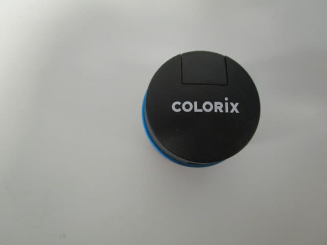
Click to zoom
Application Details
- Equipment Class
- DTS - Digital Transmission System
- Date of Grant
- Aug 30, 2023
- Application Purpose
- Original Equipment
- Date of Application
- Aug 30, 2023
- Equipment Note
- Colorcatch Nano 2
- Frequency Range
- 2402.00000000 - 2480.00000000
- Company
- Colorix SA
- Country
- Switzerland
Documents & Files
Document Text
Text extracted from the exhibit documents filed with the FCC. Open a document above to read the original.
Users Manual
USER GUIDE Start the App that is compatible with your NANO 2 and go to the NANO menu. Now switch on the NANO 2 by pressing its button for 3 seconds. Then simply follow the instructions in the App. To charge the NANO 2's battery connect the USB-C cable to a USB-C or USB charger. The NANO 2 is fully charged when the light around the connector turns from red to green. A full charge can last up to 6 hours. GUIDE D’UTILISATION Lancez l'app compatible avec votre NANO 2 et allez dans le menu NANO. Allumez ensuite le NANO 2 en appuyant sur son bouton pendant 3 secondes. Ensuite, suivez simplement les instructions dans l'app. Pour recharger la batterie du NANO 2 connectez le câble USB-C à un chargeur USB-C ou USB. Le NANO 2 est complètement chargé lorsque la lumière autour du connecteur passe du rouge au vert. Une recharge complète peut durer jusqu’à 6 heures de temps. BENUTZERHANDBUCH Starten Sie die mit Ihrem NANO 2 kompatible App und gehen Sie in das NANO-Menü. Schalten Sie dann den NANO 2 ein, indem Sie seine Taste 3 Sekunden lang gedrückt halten. Folgen Sie dann einfach den Anweisungen der App. Um den Akku des NANO 2 aufzuladen, schließen Sie das USB-C-Kabel an ein USB-C- oder USB-Ladegerät an. Der NANO 2 ist vollständig aufgeladen, wenn das Licht um den Anschluss herum von rot auf grün wechselt. Eine komplette Aufladung kann bis zu 6 Stunden dauern. COLORCATCH NANO 2 is Made for: Apple devices running iOS 15 or later | Android devices running Marshmallow (6.0) or later | Bluetooth ® 5.0 or later Includes: NANO 2, a protective case, a USB-C to USB-C cable and a USB-C to USB adapter for battery charging. COLORCATCH NANO 2 Designed by Colorix SA in Neuchâtel. Assembled in Switzerland. © 2023 Colorix SA. All rights reserved. To comply with ISED and FCC RF Exposure compliance requirements, this device must be used in such a manner to allow all persons to maintain a minimum separation distance of 20 cm from the device and its internal antenna while in operation.
Attestation Statements
Federal Communications Commission Authorization and Evaluation Division 7435 Oakland Mills Road Columbia, MD 21046 USA Neuchâtel, August 9 th 2023 Ref: Attestation Statements Part 2.911(d)(7) Filing FCC ID: 2BCAM-NANO2 FRN: 0034061853 Colorix SA (“the applicant”) certifies that, as of the date of the filing of the application, DXL Enterprises, Inc. is our designated U.S. agent for service of process for the above referenced FCC ID. Colorix SA accepts to maintain an agent for no less than one year after the grantee has terminated all marketing and importation or the conclusion of any Commission-related proceeding involving the equipment. DXL Enterprises, Inc. accepts, as of the date of the filing of the application, the obligation of the designated U.S. agent for service of process for the above referenced FCC ID. Designated U.S. Agent Information: Name: DXL Enterprises, Inc. FRN: 0034151225 Address: 575 Corporate Drive, Lobby 4, S uite 4200, Mahwah, NJ 07430 Contact Person: Cyrill Villemin Tel.: +1 201 574 5403 Email: [email protected] Sincerely, Colorix SA DXL Enterprises, Inc. David Maurer Cyrill Villemin
Attestation Statements
Federal Communications Commission Authorization and Evaluation Division 7435 Oakland Mills Road Columbia, MD 21046 USA Neuchâtel, August 9 th 2023 Ref: Attestation Statements Part 2.911(d)(5)(ii) Filing FCC ID: 2BCAM-NANO2 Colorix SA (“the applicant”) certifies that, as of the date of the filing of the application, the applicant is not identified on the Covered List (as a specifically named entity or any of its subsidiaries or affiliates) as an entity producing “covered” equipment. Best regards, David Maurer CEO & Founder
Attestation Statements
Federal Communications Commission Authorization and Evaluation Division 7435 Oakland Mills Road Columbia, MD 21046 USA Neuchâtel, August 9 th 2023 Ref: Attestation Statements Part 2.911(d)(5)(i) Filing FCC ID: 2BCAM-NANO2 Colorix SA (“the applicant”) certifies that the equipment for which authorization is sought is not "covered" equipment prohibited from receiving an equipment authorization pursuant to section 2.903 of the FCC Rules.d Best regards, David Maurer CEO & Founder
Cover Letter(s)
Timco Engineering, Inc. 849 N.W. State Road 45 P.O. Box 370 Newberry, FL 32669 U.S.A Neuchâtel, August 7 th 2023 SUBJECT: Application(s) for Certification for FCC ID: 2BCAM-NANO2 IC: 31069-NANO2 Device: COLORCATCH NANO 2 To Whom It May Concern: We, the undersigned, hereby authorize Sharon Hoffman at TIMCO ENGINEERING, INC. on our behalf, to apply for certification on our equipment referenced above. Any and all acts carried out by TIMCO ENGINEERING, INC. on our behalf shall have the same effect as acts of our own. This is to advise that we are in full compliance with the Anti- Drug Abuse Act. We, the applicant, are not subject to a denial of federal benefits pursuant to Section 5301 of the Anti-Drug Act of 1988, 21 USC853a, and no party to the application is subject to a denial of federal benefits pursuant to that section. Best regards, David Maurer CEO & Founder
Cover Letter(s)
Federal Communications Commission Authorization and Evaluation Division 7435 Oakland Mills Road Columbia, MD 21046 USA Neuchâtel, August 7 th 2023 Confidentiality Request regarding application for certification of FCC ID: 2BCAM- NANO2 and IC: 31069-NANO2 Pursuant to Sections 0.457 and 0.459 of the Commission’s Rules, we hereby request confidential treatment of information accompanying this application as outlined below: Exhibit Type Schematics Block Diagram Circuit Description The above materials contain trade secrets an d proprietary information not customarily released to t he public. The public disclosure of these materials may be harmful to t he applicant and provide unjustified benefits to its competitors. The applicant understands that pursuant to Section 0.457 of the Rules, disclosure of this application and all accompanying documentation will not be made before the date of the Grant for this application. Pursuant to DA04-1705 June 15, 2004 of t he Commission’s public notice, we also request temporary confidential tr eatment of information accompanying this application as outlined below for 180 days: Exhibit Type External Photos Internal Photos Test set up Photos User manual Best regards, David Maurer CEO & Founder
Cover Letter(s)
COLORIX SA FCC ID: 2BCAM-NANO2 IC: 31069-NANO2 The user guide for this product is located on the Box Botom of the box that the device comes in. The warning statements will be inside of the box as an insert (see example below).
ID Label/Location Info
COLORIX SA FCC ID: 2BCAM-NANO2 IC: 31069-NANO2 LABEL SAMPLE AND LOCATION LABEL SAMPLE: LABEL LOCATION (Botom of Device) FCC ID: 2BCAM-NANO2 IC: 31069-NANO2 NANO 2
Internal Photos
Internal Photos: Best regards, David Maurer CEO & Founder Internal photo with antenna loca�on marked
RF Exposure Info
Test Report# TR_9271-23_FCC 1.1310/ MPE_ Revision: 1 An IIA Company Te s t Report - FCC Par t 1.1310/ MPE Applicant: Colorix SA Approved for Release By: Signature: Name & Title: Bruno Clavier, General Manager Date of Signature 8/28/2023 This test report shall not be reproduced except in full without the written and signed permission of Timco Engineering Inc. (IIA). This test report relates only to the items tested as identified and is not valid for any subsequent changes or modifications made to the equipment under test. Timco Engineering, Inc., an IIA Company 849 NW State Road 45, Newberry, Florida 32669 (352) 472-5500 / [email protected] Page 2 of 10 This test report shall not be reproduced except in full without the written and signed permission of Timco Engineering Inc. (IIA). Table of Contents 1. APPLICANT INFORMATION ........................................................................................................................................................................... 3 2. LOCATION OF TESTING ................................................................................................................................................................................. 3 2.1 TEST LABORATORY .................................................................................................................................................................................................... 3 2.2 TESTING WAS PERFORMED, REVIEWED BY ................................................................................................................................................................4 3. TEST SAMPLE(S) (EUT/DUT) ........................................................................................................................................................................... 5 3.1 DESCRIPTION OF THE EUT ........................................................................................................................................................................................ 5 4. TEST METHODS & APPLICABLE REGULATORY LIMITS ............................................................................................................................ 6 4.1 TEST METHODS/STANDARDS/GUIDANCE: ............................................................................................................................................................... 6 4.1.1 FCC Limits for Maximum Permissible Exposure (MPE) .................................................................................................................. 6 4.2 EQUATIONS................................................................................................................................................................................................................ 7 5. RF EXPOSURE RESULTS .................................................................................................................................................................................. 8 6. HISTORY OF TEST REPORT CHANGES ........................................................................................................................................................ 9 Timco Engineering, Inc., an IIA Company 849 NW State Road 45, Newberry, Florida 32669 (352) 472-5500 / [email protected] Page 3 of 10 This test report shall not be reproduced except in full without the written and signed permission of Timco Engineering Inc. (IIA). 1. Applicant Information Applicant: Colorix SA Address: Route des Falaises 140 Neuchatel, 2000, Switzerland 2. Location of Testing 2.1 Test Laboratory Timco Engineering Inc. is a subsidiary of Industrial Inspection & Analysis, Inc. (“IIA”). Testing was performed at Timco’s permanent laboratory located at 849 NW State Road 45, Newberry, Florida 32669 FCC test firm # 578780 FCC Designation # US1070 FCC site registration is under A2LA certificate # 0955.01 ISED Canada test site registration # 2056A EU Notified Body # 1177 For all designations see A2LA scope # 0955.01 Timco Engineering, Inc., an IIA Company 849 NW State Road 45, Newberry, Florida 32669 (352) 472-5500 / [email protected] Page 4 of 10 This test report shall not be reproduced except in full without the written and signed permission of Timco Engineering Inc. (IIA). 2.2 Testing was performed, reviewed by Dates of Testing: 7/28/2023 – 8/3/2023 Signature: Name & Title: Tim Royer, EMC Engineer Date of Signature 8/28/2023 Signature: Name & Title: Kristoffer Costa, EMC Technician Date of Signature 8/28/2023 Timco Engineering, Inc., an IIA Company 849 NW State Road 45, Newberry, Florida 32669 (352) 472-5500 / [email protected] Page 5 of 10 This test report shall not be reproduced except in full without the written and signed permission of Timco Engineering Inc. (IIA). 3. Test Sample(s) (EUT/DUT) The test sample was received: 7/28/2023 3.1 Description of the EUT A description as well as unambiguous identification of the EUT(s) tested. Where more than one sample is required for technical reasons (such as the use of connected units for the purpose of conducted output power testing where the product units will have integral antennas), each specific test shall identify which unit was tested. Identification FCC ID: 2BCAM-NANO2 Brief Description Colorcatch Nano 2 Model(s) # NANO 2 Firmware version 5.4.6 Hardware version and Stack 4.4.1 5.4.5 Serial Number 623XXXXXX Technical Characteristics Frequency Range 2400 MHz- 2483.5 MHz RF O/P Power (Max.) -17.80 dBm/ 0.0000166 W Modulation FM Bandwidth & Emission Class N/A Number of Channels N/A Duty Cycle 100% Antenna Connector N/A Voltage Rating (AC or Batt.) 5 VDC Antenna Characteristics Antenna Frequency Range Mode / BW Antenna Gain 1 n/a n/a 0 dBi - Note: Information such as antenna gain, firmware/software numbers are provided by manufacturer and cannot be validated by the test lab. Timco Engineering, Inc., an IIA Company 849 NW State Road 45, Newberry, Florida 32669 (352)…
Text truncated - open the document above for the full version.
Test Report
Test Report# TR_9271-23_FCC 15.247 DTS_ Revision: 1 An IIA Company Te s t Report - FCC Par t 15.247/ DTS Applicant: Colorix SA Approved for Release By: Signature: Name & Title: Bruno Clavier, General Manager Date of Signature 8/28/2023 This test report shall not be reproduced except in full without the written and signed permission of Timco Engineering Inc. (IIA). This test report relates only to the items tested as identified and is not valid for any subsequent changes or modifications made to the equipment under test. Timco Engineering, Inc., an IIA Company 849 NW State Road 45, Newberry, Florida 32669 (352) 472-5500 / [email protected] Page 2 of 38 This test report shall not be reproduced except in full without the written and signed permission of Timco Engineering Inc. (IIA). Table of Contents 1. APPLICANT INFORMATION ........................................................................................................................................................................... 4 1.1 TEST RESULT SUMMARY ............................................................................................................................................................................................4 2. LOCATION OF TESTING ................................................................................................................................................................................. 6 2.1 TEST LABORATORY .................................................................................................................................................................................................... 6 2.2 TESTING WAS PERFORMED, REVIEWED BY ................................................................................................................................................................ 6 3. TEST SAMPLE(S) (EUT/DUT) ........................................................................................................................................................................... 7 3.1 DESCRIPTION OF THE EUT ........................................................................................................................................................................................ 7 3.2 CONFIGURATION OF EUT ......................................................................................................................................................................................... 8 3.3 TEST SETUP OF EUT .................................................................................................................................................................................................. 8 4. TEST METHODS & APPLICABLE REGULATORY LIMITS ............................................................................................................................ 9 4.1 TEST METHODS/STANDARDS/GUIDANCE: ............................................................................................................................................................... 9 4.2 APPLIED LIMITS AND REGULATORY LIMITS: .............................................................................................................................................................. 9 5. MEASUREMENT UNCERTAINTY .................................................................................................................................................................... 9 6. ENVIRONMENTAL CONDITIONS ................................................................................................................................................................. 9 6.1 TEMPERATURE & HUMIDITY ...................................................................................................................................................................................... 9 7. LIST OF TEST EQUIPMENT AND TEST FACILITY ...................................................................................................................................... 10 7.1 LIST OF TEST EQUIPMENT ....................................................................................................................................................................................... 10 8. TEST RESULTS .................................................................................................................................................................................................. 11 8.1 DTS CONDUCTED OUTPUT POWER ........................................................................................................................................................................ 12 8.1.1 Conducted Output Power, 2402 MHz .............................................................................................................................................. 13 8.1.2 Conducted Output Power, 2426 MHz .............................................................................................................................................. 14 8.1.3 Conducted Output Power, 2480 MHz .............................................................................................................................................. 15 8.2 OCCUPIED BANDWIDTH .......................................................................................................................................................................................... 16 8.2.1 99% Bandwidth Plot, 2402 MHz ........................................................................................................................................................ 17 8.2.2 99% Bandwidth Plot, 2426 MHz ........................................................................................................................................................ 18 8.2.3 99% Bandwidth Plot, 2480 MHz ..................................................................................................................................…
Text truncated - open the document above for the full version.
Test Report
www.cypress.com Document No. 001-91445 Rev. *H 1 AN91445 Antenna Design and RF Layout Guidelines Authors: Tapan Pattnayak, Guhapriyan Thanikachalam Associated Part Family: CY8C4XXX-BL, CYBL1XXXX, CY8C6XXXXX-BL Related Application Notes: For the complete list, click here To get the latest version of this application note and the associated Gerber file, please visit http://www.cypress.com/go/AN91445 This application note is for informational purposes. Antenna design requires suitable test equipment and know-how for optimal performance. It is strongly advised that the professional services of firms specializing in the design and placement of antennas be sought out. Cypress can provide a list of suitable antenna design specialists, if requested. AN91445 explains antenna design in simple terms and provides guidelines for RF component selection, matching network design, and layout design. This application note also recommends two Cypress-tested PCB antennas that can be implemented at a very low cost for use with the Bluetooth Low Energy (BLE) solutions that are part of Cypress’s PSoC® and PRoC™ families. For information on WICED Smart BLE solutions, see the WICED community product guide page. The PRoC BLE, PSoC 4 BLE, and PSoC 6 MCU with Bluetooth Low Energy (BLE) Connectivity 2.4-GHz radio must be carefully matched to its antenna for optimum performance. Contents 1 Introduction .................................................................. 2 2 Antenna Basics ............................................................ 3 3 Antenna Types ............................................................ 4 4 Choosing an Antenna .................................................. 5 5 Antenna Parameters .................................................... 6 6 Antennas for Cypress PRoC/PSoC BLE ..................... 9 7 Cypress-Proprietary PCB Antennas ............................ 9 7.1 Meandered Inverted-F Antenna (MIFA) ............ 10 7.2 Antenna Feed Consideration ............................ 11 7.3 Antenna Length Considerations ........................ 14 7.4 Inverted-F Antenna (IFA) .................................. 15 8 Chip Antennas ........................................................... 17 9 Wire Antennas ........................................................... 19 10 Antenna Comparison ................................................. 20 11 Effect of Enclosure and Ground Plane on Antenna Performance ........................................... 21 11.1 Effect of Ground Plane ...................................... 21 11.2 Effect of Enclosure ............................................ 22 12 Guidelines for Antenna Placement, Enclosure, and Ground Plane.................................... 23 13 RF Concepts and Terminologies ............................... 24 13.1 Smith Chart ....................................................... 27 14 Impedance Matching ................................................. 29 14.1 Matching Network Topology .............................. 31 14.2 Tips for Matching Network ................................ 35 15 Antenna Tuning ......................................................... 35 15.1 Tuning Procedure ............................................. 36 16 RF Transmission Lines .............................................. 43 16.1 Microstrip Line .................................................. 43 16.2 CPWG (with Bottom Ground) ............................ 44 16.3 RF Trace Layout Considerations ...................... 44 17 PCB Stackup ............................................................. 46 17.1 Four-Layer PCB ................................................ 46 17.2 Two-Layer PCB ................................................ 46 18 Ground Plane ............................................................ 47 18.1 Ground Plane Considerations ........................... 47 19 Power Supply Decoupling ......................................... 47 19.1 Power Supply Decoupling Layout Considerations ...................................... 48 20 Vias .......................................................................... 48 21 Capacitors and Inductors........................................... 49 21.1 Capacitors ......................................................... 49 21.2 Inductors ........................................................... 51 22 Design for Testability ................................................. 52 23 Support for External Power Amplifier/ Low-Noise Amplifier/RF Front End ............................ 53 24 Support for Coexistence with Wi-Fi ........................... 53 24.1 Spatial Isolation ................................................ 53 24.2 Frequency Isolation .......................................... 54 24.3 Temporal Isolation ............................................ 55 25 Summary ................................................................... 55 26 Related Application Notes ......................................... 56 Appendix A. Checklist ............................................... 57 Appendix B. References ........................................... 58 Antenna Design and RF Layout Guidelines www.cypress.com Document No. 001-91445 Rev. *H 2 1 Introduction Antenna design and RF layout are critical in a wireless system that transmits and receives electromagnetic radiation in free space. The wireless range that an end-customer gets out of an RF product with a current-limited power source such as a coin-cell battery depends greatly on the antenna design, the enclosure, and a good PCB layout. It is not uncommon to have a wide variation in RF ranges for designs that use the same silicon and the same power but a different layout and antenna-design practice. This application note describes the best practices, layout guidelines, and an antenna-tuning procedure to get the widest range with a given amount of power. Other important general layout considerations for RF trace, power supply decoupling, via holes, PCB …
Text truncated - open the document above for the full version.
Test Setup Photos
ANNEX B – Test Setup Photograph Exhibit Colorix SA FCC ID: 2BCAM-NANO2 Conducted Test Setup Radiated Testing, Table Setup Radiated Testing, Above 1 GHz
Contact Information
Applicant
David Maurer(CEO)
Test Firm
Timco Engineering, Inc.Bruno Clavier
Technical Specifications
| # | Rule Parts | Frequency Range | Power Output |
|---|---|---|---|
| 1 | 15C | 2.40 GHz - 2.48 GHz | 16.60 µW |