2BCIH-K20KIDS WIRELESS OPEN-EAR HEADPHONES
Shenzhen Jiangbiao E-Commerce Co., Ltd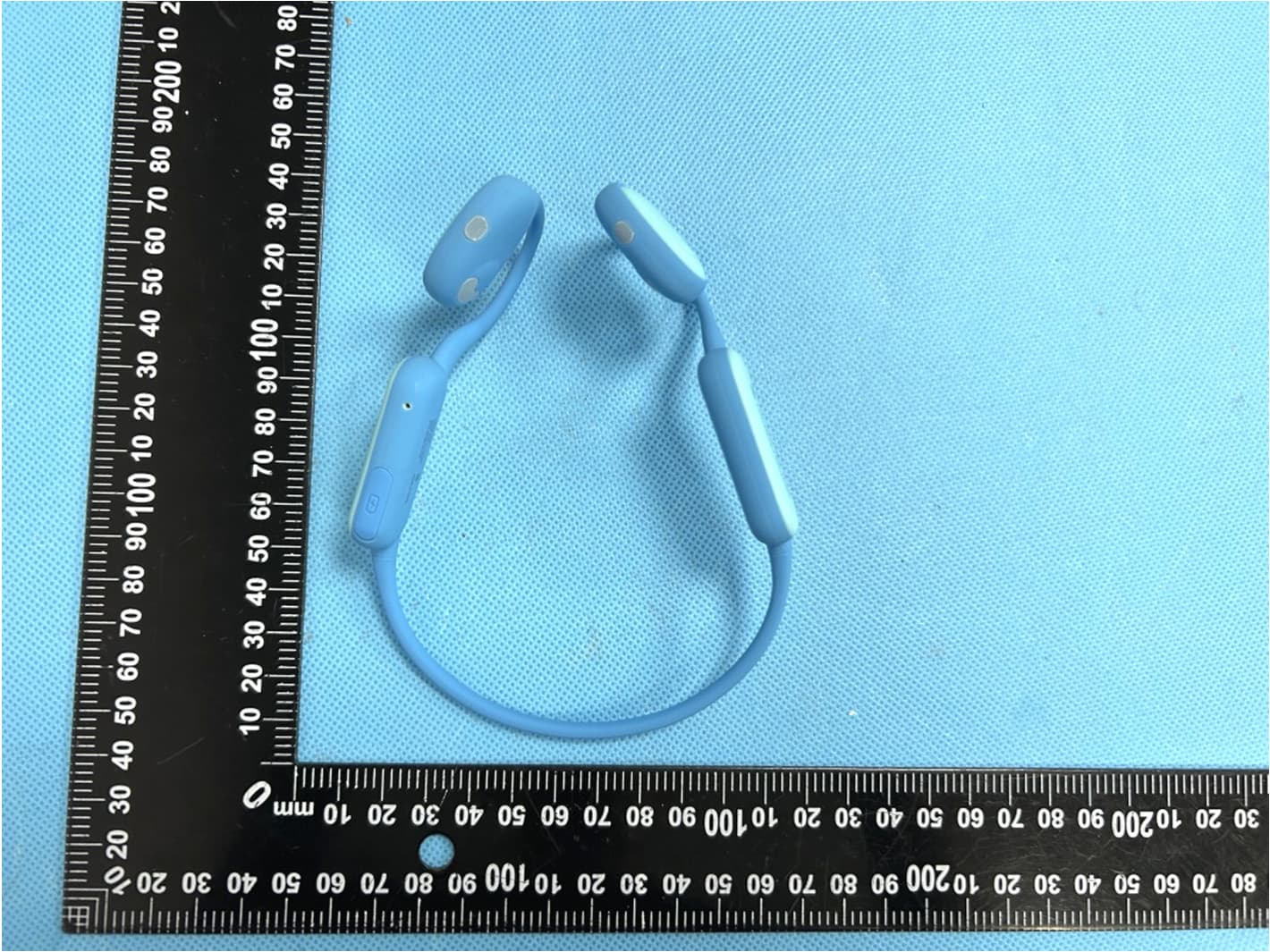
Click to zoom
Application Details
- Equipment Class
- DSS - Part 15 Spread Spectrum Transmitter
- Date of Grant
- Aug 30, 2023
- Application Purpose
- Original Equipment
- Date of Application
- Aug 30, 2023
- Equipment Note
- KIDS WIRELESS OPEN-EAR HEADPHONES
- Frequency Range
- 2402.00000000 - 2480.00000000
- Country
- China
Documents & Files
Document Text
Text extracted from the exhibit documents filed with the FCC. Open a document above to read the original.
Users Manual
Decr ease v olume: Short press " - " Previous Song: Long press " - " for 2 seconds. Incr ease v olume: Short press "+ " Next Song: Long press " + " for 2 seconds. Play/pause music: Short press power button. (Playing: No indicator light, Pausing: White indicator light) KIDS WIREL ESS OPEN-EAR HEADPHONES USER MANUAL V1.0 Wha t' s in the box : Ho w It Works 1 × User Manual1 × Soft P ouch1 × Charging Cable1 × K20 Headphones Description Of Part s Power Button Volume Up and Next Song Volume Down and Previous Song LED Indicator Type -C Charging Port Micr ophones Power On/Off Power On: Press and hold the power button f or 2 sec onds to turn on. Power Off: Press and hold the power button f or 2 sec onds to turn off. Auto Power Off: If not connected to a playback device after power on, the headphones will automatically power off after 3 minutes. Pr ess and hold for 2 seconds Blue too th P airing 2. Go to y our devic e' s Bluetoo th se ttings and connect t o " HINERSOUND K20", the indic ator light will stay white and promp t v oic e will say " Bluetoo th c onnected. " 3. To disconnect the Bluetooth: Pause the Bluetooth device's play, simultaneously press and hold the" + "and "- "buttons for 3 seconds to disconnect the Bluetooth connection. The indicator light will flash red and white alternately and prompt voice will say " Bluetooth disconnected." Volume Control / Music Control Answ er /End A Call: Short press power button. Rejec t A Call/Switch be tw een phone and earphone (during an ongoing call): Long press the power but ton f or 1.5 seconds. When the headphones have lo w batter y, the indicator light will flash red e ver y 10 seconds, ac comp anied by the promp t "Battery level low,Please recharge headset." U se a USB T ype -C char ging cable to charge the headphones . The red light will remain illuminated during charging and will turn white when fully charged. Call Func tions Char ging Instruc tions To switch be tw een sound modes: While the headphones are po wer ed on, double-click the power but ton t o alt erna te be tw een Outdoor Mode(94dB), Kids Mode(85dB) and Toddler Mode(70dB). Swit ching Sound Modes Steps1. Turn on the headphones . Connect the headphones to De vic e A. Steps2. Disconnect the headphones from Devic e A. The headphones will enter int o p airing mode. Steps3. Connect the headphones to De vic e B. Steps4. Manually rec onnect the headphones to De vic e A. Dual Devic e C onnection Func tion Specifications Pr emium 16.2MM Dynamic Driver * 2 Input :5 V 100mA Frequency R esponse: 20Hz-20KHz Blue too th V er sion : Support Bluetoo th V5.3 Blue too th T ransmitter F requency R ang e: 2400-2483.5MHZ Blue too th T ransmitter Modulation: -96dBm@GFSK, -95.5dBm@π/4 DQPSK, -88.5dBm@8DPSK modulation Ba tter y T ype: Lithium-ion Polymer (3.7V, 110mAH) Bluetooth range: 10 m/ 32.8 ft No te: Please r ead c ar efully the follo wing informa tion befor e using it. Usag e Environment: Ba tter y and Charging: Rep air s and Protec tion: Saf ety Inf orma tion Technical Support -Email: [email protected] -Website: www.hinersound.com @ Hinersound_official @ hinersound @ Hinersound @ hinersound_official 技术要求: 1. 工艺:风琴折纸; 2. 材质:128g双铜纸,单面过哑膜; 3. 印刷:四色印刷; 4. 尺寸:成型尺寸:432 * 145mm;单页尺寸:108 * 145mm; • This produc t and its ac cessories may cont ain smallpart s . Children under 14 year s old should use the pr oduc t under adult supervision. • All pack aging materials, such as tapes, trays, labels, etc., ar e no t p art of the produc t and are no t suit able for children' s play. Ple ase handle these pack aging materials properly. Warning: This equipment complies with the FCC r adia tion exposure limits se t f orth f or an uncontr olled envir onment. This transmitter must no t be c o-loc ated or operating in conjunction with any other ant enna or transmitter . RF e xpo sur e s tatement This device c omplies with Part 15 of the FCC Rules. Operation is subject t o the follo wing two conditions: (1) This devic e may not c ause harmful interf er enc e, and (2) this devic e must accept any interf er enc e rec eiv ed, including interf er enc e tha t may cause undesired operation. No te: This equipment has been tes ted and found to c omply with the limits f or a Class B digital devic e, pursuant to p art 15 of the FCC Rules. These limits ar e designed to pr ovide reasonable pr otec tion agains t harmful interf er enc e in a residential installa tion. This equipment gener ates, uses and c an r adia te r adio frequency energy and, if not ins talled and used in accor danc e with the ins truc tions, may cause harmful interf er enc e t o r adio communications. Howev er , ther e is no guar ant ee that int erf er enc e will not oc cur in a particular installa tion. If this equipment does cause harmful interf er enc e t o r adio or television rec ep tion, which can be determined by turning the equipment off and on, the user is encour ag ed t o tr y t o c orr ec t the interf er enc e b y one or more o f the follo wing measur es: —R eorient or reloc ate the rec eiving antenna. —Increase the separ ation betw een the equipment and rec eiv er . —Connect the equipment into an outlet on a circuit differ ent fr om that t o which the rec eiv er is connected. —Consult the dealer or an experienced r adio/TV technician for help. NO TE 2: Any changes or modifications to this unit not e xpr essly approved b y the party r esponsible for c ompliance c ould void the user's authority to operate the equipment. FCC W arning • T o av oid hearing damage, do not lis ten f or e xtended periods at high volume. • Do not turn the volume so high that y ou'r e unable to he ar y our surroundings. • Do not use earphones while driving. • Y ou should use caution or temporarily discontinue use in potentially hazar dous situations. He aring Safety Disclaimer: This manual is subject to update without notice. Electronic download address: www.hinersound.com KIDS WIRELESS OPEN-EAR HEADPHONES 1. When using for the first time, press and hold the power button unt…
Text truncated - open the document above for the full version.
External Photos
Reference No.: WTX23X08177568W001 Page 2 of 12 Waltek Testing Group (Shenzhen) Co., Ltd. Http://www.waltek.com.cn EXHIBIT 2 - EUT EXTERNAL PHOTOGRAPHS EUT View 1 EUT View 2 Reference No.: WTX23X08177568W001 Page 3 of 12 Waltek Testing Group (Shenzhen) Co., Ltd. Http://www.waltek.com.cn EUT View 3 EUT View 4 Reference No.: WTX23X08177568W001 Page 4 of 12 Waltek Testing Group (Shenzhen) Co., Ltd. Http://www.waltek.com.cn EUT View 5 EUT View 6 Reference No.: WTX23X08177568W001 Page 5 of 12 Waltek Testing Group (Shenzhen) Co., Ltd. Http://www.waltek.com.cn EUT View 7
ID Label/Location Info
Reference No.: WTX23X08177568W001 Page 1 of 12 Waltek Testing Group (Shenzhen) Co., Ltd. Http://www.waltek.com.cn ANNEX EXHIBIT 1 - PRODUCT LABELING Proposed FCC ID Label Format Specifications: The label shall be securely affixed to a permanently attached part of the device, in a location where it is visible or easily accessible to the user, and shall not be readily detachable. The label shall be sufficiently durable to remain fully legible and intact on the device in all normal conditions of use throughout the device’s expected lifetime. Proposed Label Location on EUT FCC ID Label Location
Internal Photos
Reference No.: WTX23X08177568W001 Page 6 of 12 Waltek Testing Group (Shenzhen) Co., Ltd. Http://www.waltek.com.cn EXHIBIT 3 - EUT INTERNAL PHOTOGRAPHS EUT Housing and Board View 1 Solder Board-Component View 1 Reference No.: WTX23X08177568W001 Page 7 of 12 Waltek Testing Group (Shenzhen) Co., Ltd. Http://www.waltek.com.cn Solder Board-Component View 2 Solder Board-Component View 3 Reference No.: WTX23X08177568W001 Page 8 of 12 Waltek Testing Group (Shenzhen) Co., Ltd. Http://www.waltek.com.cn Solder Board-Component View 4 Solder Board-Component View 5 Reference No.: WTX23X08177568W001 Page 9 of 12 Waltek Testing Group (Shenzhen) Co., Ltd. Http://www.waltek.com.cn Antenna View BT Antenna
RF Exposure Info
RF Exposure Requirements Product Description: KIDS WIRELESS OPEN-EAR HEADPHONES Model No.: K20 FCC ID: 2BCIH-K20 According to the KDB 447498 D01 v06 section 4.3.1, for 100 MHz to 6 GHz and test separation distances ≤ 50 mm, the 1-g and 10-g SAR test exclusion thresholds are determined by the following: [(max. power of channel, including tune-up tolerance, mW)/(min. test separation distance, mm)] · [√f(GHz)] ≤ 3.0 for 1-g SAR and ≤ 7.5 for 10-g extremity SAR, where - f(GHz) is the RF channel transmit frequency in GHz - Power and distance are rounded to the nearest mW and mm before calculation - The result is rounded to one decimal place for comparison Calculation Result: Tx frequency range: 2402-2480MHz Min. test separation distance: 5mm Maximum Conducted Output Power: 5.44dBm Tune-Up output power: 6.0dBm RF channel transmit frequency: 2480MHz Result: 1.2 Limit: 3.0 The exclusion thresholds is 1.2 < 3, so the transmitter complies with the RF exposure requirements and the SAR is not required.
Test Report
Features 1.Surface Mounted Devices with a small dimension of 2.0 x 1.25 x 0.25 mm 3 meet future miniaturization trend. 2.Embedded and (Low Temperature Co-fired Ceramic) technology is able to future integratewith system design as well as beautifying the housing of final product. 3.High Stability in Temperature / Humidity Change Applications 1. Bluetooth 2. Wireless LAN 3. HormRF 4. ISM band 2.4GHz wireless applications Dimensions(Unit:mm) H L X 20125025 A03 Dimension (mm) L 2.0 ± 0.20 W 1.2 ± 0.20 T 0.25 ± 0.05 Manufacturer: SHENZHEN HELIXUN TECHNOLOGY CO., LTD Address: 1905, Building 2, Jiufang Square, Tie Zai Road, Gongle Community, Xixiang Street, Bao'an District, Shenzhen Type2 : H L X 20125025 A03 Type1 : Type2 : PCB Bottom View : H L X 20125025 A03 Evaluation Board and Matching Circuits Electrical Characteristics H L X 20125025 A03 Specification H L X 2 0 1 2 5 0 2 5 A03 Central Frequency2450MHz Bandwidth90 (Min.)MHz Return Loss-10 (Max)dB Peak Gain2.11dBi Impedance50 Ω Operating Temperature -40~+85 °C Maximum Power1W Resistance to Soldering Heats 10 ( @ 260°C) sec. PolarizationLinear Azimuth BeamwidthOmni-directional TerminationCu / Sn (Leadless) Characteristic curve Radiation Pattern H L X 20125025 A03 Frequency (MHz)240024502500 Efficiency (dB)-1.42-1.24-1.47 Efficiency (%)717571 Peak Gain (dBi)2.112.061.94 Phase Temperature(°C) Time(min) 1 +85±5°C 30±3 2 Room Temperature Within 3sec 3 -40±2°C 30±3 4 Room Temperature Within 3sec ITEMREQUIREMENTSTEST CONDITION Solderability 1.Wetting shall exceed 90% coverage 2.No visible mechanical damage TEMP (°C) 230°C 4±1 sec. 150°C 60sec Pre-heating temperature:150°C/60sec. Solder temperature:230±5°C Duration:4±1sec. Solder:Sn-Ag3.0-Cu0.5 Flux for lead free: rosin Solder heat Resistance 1.No visible mechanical damage 2.Central Freq. change :within ± 6% TEMP (°C) 260°C 10±0.5 sec. 150°C 60sec Pre-heating temperature:150°C/60sec. Solder temperature:260±5°C Duration:10±0.5sec. Solder:Sn-Ag3.0-Cu0.5 Flux for lead free: rosin Component Adhesion (Push test) 1. No visible mechanical damageThe device should be reflow soldered(230±5°C for 10sec.) to a tinned copper substrate A dynometer force gauge should be applied the side of the component. The device must with-ST-F 0.5 Kg without failure of the termination attached to component. Component Adhesion (Pull test) 1. No visible mechanical damage Insert 10cm wire into the remaining open eye bend ,the ends of even wire lengths upward and wind together. Terminal shall not be remarkably damaged. Thermal shock 1.No visible mechanical damage 2.Central Freq. change :within ±6% +85°C=>30±3min -40°C=>30±3min Test cycle:10 cycles The chip shall be stabilized at normal condition for 2~3 hours before measuring. Resistance to High Temperature 1.No visible mechanical damage 2.Central Freq. change :within ±6% 3.No disconnection or short circuit. Temperature: 85±5°C Duration: 1000±12hrs The chip shall be stabilized at normal condition for 2~3 hours before measuring. Resistance to Low Temperature 1.No visible mechanical damage 2.Central Freq. change :within ±6% 3.No disconnection or short circuit. Temperature:-40±5°C Duration: 1000±12hrs The chip shall be stabilized at normal condition for 2~3 hours before measuring. Humidity 1.No visible mechanical damage 2.Central Freq. change :within ±6% 3.No disconnection or short circuit. Temperature: 40±2°C Humidity: 90% to 95% RH Duration: 1000±12hrs The chip shall be stabilized at normal condition for 2~3 hours before measuring. H L X 20125025 A03 Reliability and Test Condictions Recommended temperature profiles for re-flow soldering in Figure 1. Products attachment with a soldering iron is discouraged due to the inherent process control limitations. In the event that a soldering iron must be employed the following precautions are recommended. ‧Preheat circuit and products to 150°C ‧Never contact the ceramic with the iron tip ‧Use a 20 watt soldering iron with tip diameter of 1.0mm ‧280°C tip temperature (max) ‧1.0mm tip diameter (max) ‧Limit soldering time to 3 sec. NATURAL C OOLING PRE- HEATING 60~120 s SOLDERING 10s max. 30~60s 250~260 230 180 150 TIME(sec.) Reflow Soldering NATURAL COOLING PRE-HEATINGSOLDERING within 3s Gradual cooling 150 TIME(sec.) Iron Soldering Over 60s 350 300 H L X 20125025 A03 Soldering and Mounting Mildly activated rosin fluxes are preferred. The minimum amount of solder can lead to damage from the stresses caused by the difference in coefficients of expansion between solder, chip and substrate. The terminations are suitable for all wave and re-flow soldering systems. If hand soldering cannot be avoided, the preferred technique is the utilization of hot air soldering tools. ◆Reel Specification: (7’’, Φ180 mm) Tape Width(mm)A(mm)B(mm)C(mm)D(mm)Chip/Reel(pcs) 8 9.0±0.560±213.5±0.5178±2 6000 H L X 20125025 A03 Packaging Information ◆Tape Specification: H L X 20125025 A03 Storage and Transportation Information Storage Conditions To maintain the solderability of terminal electrodes: 1.Temperature and humidity conditions: -10~ 40°C and 30~70% RH. 2.Recommended products should be used within 6 months from the time of delivery. 3.The packaging material should be kept where no chlorine or sulfur exists in the air. Transportation Conditions 1.Products should be handled with care to avoid damage or contamination from perspiration and skin oils. 2.The use of tweezers or vacuum pick up is strongly recommended for individual components. 3.Bulk handling should ensure that abrasion and mechanical shock are minimized.
Test Report
Waltek Testing Group (Shenzhen) Co., Ltd. Http://www.waltek.com.cn Page 1 of 64 TEST REPORT Reference No. .................... : WTX23X08177568W001 FCC ID ................................ : 2BCIH-K20 Applicant ........................... : Shenzhen Jiangbiao E-Commerce Co.,Ltd Address ............................. : Room 913, Yagang Industry and Trade Building, Pinghu Street, Longgang District, Shenzhen,China Manufacturer ..................... : HINERSOUND TECHNOLOGY CO., LIMITED Address ............................. : RM705, FAYUEN COMM BUILDING NO. 77 FAYYUEN STREET KL Product Name ................... : KIDS WIRELESS OPEN-EAR HEADPHONES Model No... ......................... : K20 Standards .......................... : FCC Part 15.247 Date of Receipt sample .... : 2023-08-14 Date of Test........................ : 2023-08-14 to 2023-08-24 Date of Issue ..................... : 2023-08-24 Test Report Form No. ....... : WTX_Part 15_247W Test Result ......................... : Pass Remarks: The results shown in this test report refer only to the sample(s) tested, this test report cannot be reproduced, except in full, without prior written permission of the company. The report would be invalid without specific stamp of test institute and the signatures of approver. Prepared By: Waltek Testing Group (Shenzhen) Co., Ltd. Address: 1/F., Room 101, Building 1, Hongwei Industrial Park, Liuxian 2nd Road, Block 70 Bao'an District, Shenzhen, Guangdong, China Tel.: +86-755-33663308 Fax.: +86-755-33663309 Email: [email protected] Tested by: Approved by: Dashan Chen Silin Chen Reference No.: WTX23X08177568W001 Waltek Testing Group (Shenzhen) Co., Ltd. Http://www.waltek.com.cn Page 2 of 64 TABLE OF CONTENTS 1. GENERAL INFORMATION .................................................................................................................................... 5 1.1 PRODUCT DESCRIPTION FOR EQUIPMENT UNDER TEST (EUT) ......................................................................... 5 1.2 TEST STANDARDS ................................................................................................................................................. 6 1.3 TEST METHODOLOGY ........................................................................................................................................... 6 1.4 TEST FACILITY ...................................................................................................................................................... 6 1.5 EUT SETUP AND TEST MODE .............................................................................................................................. 7 1.6 MEASUREMENT UNCERTAINTY ............................................................................................................................. 9 1.7 TEST EQUIPMENT LIST AND DETAILS ................................................................................................................. 10 2. SUMMARY OF TEST RESULTS ......................................................................................................................... 13 3. ANTENNA REQUIREMENT ................................................................................................................................. 14 3.1 STANDARD APPLICABLE ..................................................................................................................................... 14 3.2 EVALUATION INFORMATION ................................................................................................................................ 14 4. FREQUENCY HOPPING SYSTEM REQUIREMENTS .................................................................................... 15 4.1 STANDARD APPLICABLE ..................................................................................................................................... 15 4.2 FREQUENCY HOPPING SYSTEM ......................................................................................................................... 15 4.3 EUT PSEUDORANDOM FREQUENCY HOPPING SEQUENCE ............................................................................... 16 5. QUANTITY OF HOPPING CHANNELS AND CHANNEL SEPARATION .................................................... 17 5.1 STANDARD APPLICABLE ..................................................................................................................................... 17 5.2 TEST SETUP BLOCK DIAGRAM ........................................................................................................................... 17 5.3 TEST PROCEDURE .............................................................................................................................................. 17 5.4 SUMMARY OF TEST RESULTS/PLOTS ................................................................................................................. 18 6. DWELL TIME OF HOPPING CHANNEL ........................................................................................................... 19 6.1 STANDARD APPLICABLE ..................................................................................................................................... 19 6.2 TEST SETUP BLOCK DIAGRAM ........................................................................................................................... 19 6.3 TEST PROCEDURE .............................................................................................................................................. 19 6.4 SUMMARY OF TEST RESULTS/PLOTS ................................................................................................................. 20 7. 20DB BANDWIDTH ............................................................................................................................................... 21 7.1 STANDARD APPLICABLE ................................................................................................................…
Text truncated - open the document above for the full version.
Test Setup Photos
Reference No.: WTX23X08177568W001 Page 10 of 12 Waltek Testing Group (Shenzhen) Co., Ltd. Http://www.waltek.com.cn EXHIBIT 4 - TEST SETUP PHOTOGRAPHS Conducted Emission Test Setup Radiation Emission Test Setup (Below 30MHz) Reference No.: WTX23X08177568W001 Page 11 of 12 Waltek Testing Group (Shenzhen) Co., Ltd. Http://www.waltek.com.cn Radiation Emission Test Setup (30MHz to 1GHz) Radiation Emission Test Setup (1GHz to 18GHz) Reference No.: WTX23X08177568W001 Page 12 of 12 Waltek Testing Group (Shenzhen) Co., Ltd. Http://www.waltek.com.cn Radiation Emission Test Setup (Above 18GHz) ***** END OF REPORT *****
Contact Information
Applicant
Jim Zhou(Manager)
Test Firm
Waltek Testing Group (Shenzhen) Co., Ltd.Jandy So
Technical Specifications
| # | Rule Parts | Frequency Range | Power Output |
|---|---|---|---|
| 1 | 15C | 2.40 GHz - 2.48 GHz | 3.50 mW |