2BCYMHHWL-C02Truly Wireless Earbuds
Shenzhen Pipijia Technology Co., Ltd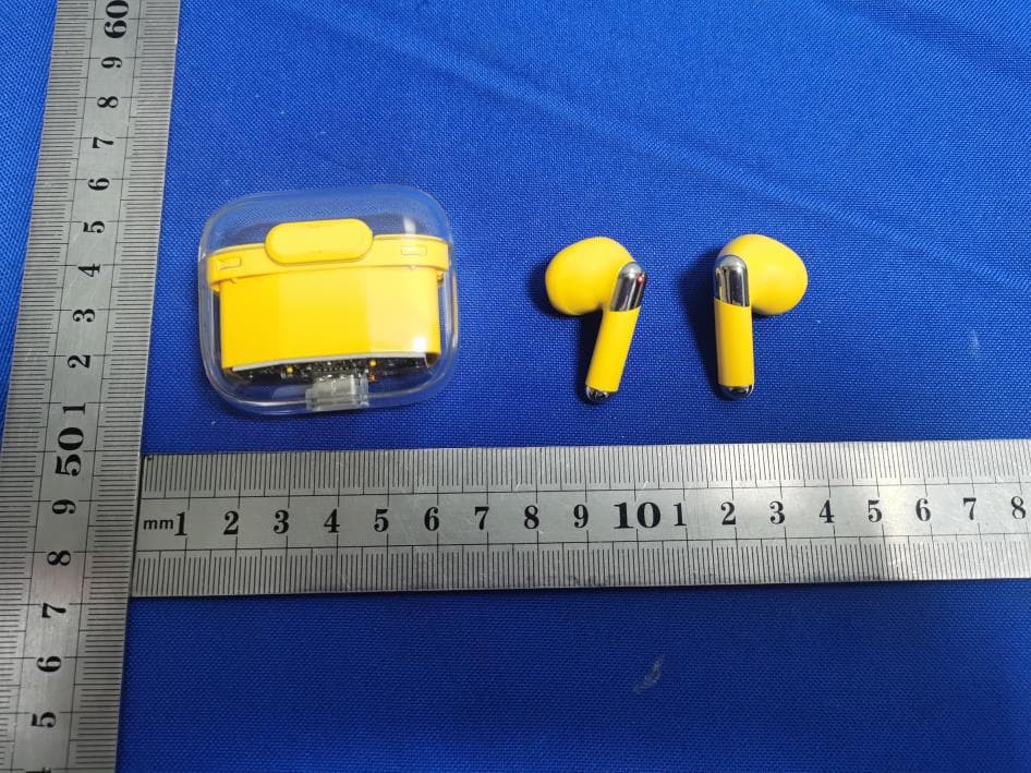
Click to zoom
Application Details
- Equipment Class
- DSS - Part 15 Spread Spectrum Transmitter
- Date of Grant
- Sep 25, 2023
- Application Purpose
- Original Equipment
- Date of Application
- Sep 25, 2023
- Equipment Note
- Truly Wireless Earbuds
- Frequency Range
- 2402.00000000 - 2480.00000000
- Country
- China
Documents & Files
Document Text
Text extracted from the exhibit documents filed with the FCC. Open a document above to read the original.
Users Manual
HHWL-C02 User Manual Thank you for purchasing and using our procuct! To improve your experience,please kindly read the user manual first. Product Specification: Product name HHWL-C02 Bluetooth version V5.3 Product compatibility Android/Apple Transmission distance 8-10M Trumpet 13 copper ring composite film Power consumption 6mAh Range 5H Charging case battery life 16H+ Standby time 180 days Charging Time 1.5H Battery capacity 30mAh*2 Battery capacity 200mAh Charging interface type Type-C Charging voltage 5V/1A Color White, black, green, blue, yellow, purple, orange, red, camel Product Overview: charging indicator Touch button Master voice control Charging port Accessories List How to Use: Turm on the device's Bluetooth and headset charging box to enter the pairing mode. Click the headset pairing name found by Bluetooth: C02 to pair. The headset will display a prompt tone to indicate successful pairing If the headset is not paired successfully within 5 minutes, it will turm off automatically. * Warning 1. Do not use corrosive detergent to clean this product. 2. Store the produet in a dry environment and charge the charging case at least once a month. 3.Please adjust the volume to the most appropriate state when using it. High volume may cause a risk of hearing loss. 4. It is forbidden to dismantle, impact or throw into fire without permision.Ifexpansion occurs, do not eontinue to use it.Do not putit in high temperature environment. Operation Instructions Left ear click pause/play Double-click on the last track Three clicks for yolume reduction Long press voice assistant Right ear click pause/play Double click on the next track Three clicks for volume Long press voice assistant Call click answer/hang up, both ears Double-click no action Three clicks left ear volume reduction Three clicks on the right ear to increase volume Long press 3 seconds to reject, both ears Maintenance instructions: This card is only valid for use in products by the warranty,as detailed below: 1.Purchasing the products through legal and formal channels; 2. Non-human damage products,including but not limited to private disassemblyimproper use,In case of natural disasters, ete,it is not covered by the warranty; 3.Notexceeding product warranty period,It includes and is not limited to the above,The company reserves the right of final interpretation. Warranty Card Customer name: Contact Number: Contact Address: Product Model: Brief description of the problem: Product certification: Inspectors: Production and inspection date; This device complies with part 15 of the FCC Rules. Operation is subject to the following two conditions: (1) this device may not cause harmful interference, and (2) this device must accept any interference received, including interference that may cause undesired operation. Any changes or modifications not expressly approved by the party responsible for compliance could void the user's authority to operate the equipment. NOTE: This equipment has been tested and found to comply with the limits for a Class B digital device, pursuant to Part 15 of the FCC Rules. These limits are designed to provide reasonable protection against harmful interference in a residential installation. This equipment generates, uses and can radiate radio frequency energy and, if not installed and used in accordance with the instructions, may cause harmful interference to radio communications. However, there is no guarantee that interference will not occur in a particular installation. If this equipment does cause harmful interference to radio or television reception, which can be determined by turning the equipment off and on, the user is encouraged to try to correct the interference by one or more of the following measures: -- Reorient or relocate the receiving antenna. -- Increase the separation between the equipment and receiver. -- Connect the equipment into an outlet on a circuit different from that to which the receiver is connected. -- Consult the dealer or an experienced radio/TV technician for help. The device has been evaluated to meet general RF exposure requirement. The device can be used in portable exposure condition without restriction
Attestation Statements
(Shenzhen Pipijia Technology Co., Ltd) (September 21, 2023) Eurofins Electrical and Electronic Testing NA, Inc. 914 West Patapsco Avenue Baltimore, MD 21230 RE: Attestation Statements Part 2.911(d)(5)(i) request for (FCC ID: 2BCYMHHWL-C02) [Shenzhen Pipijia Technology Co., Ltd] (“the applicant”) certifies that the equipment for which authorization is sought is not “covered” equipment prohibited from receiving an equipment authorization pursuant to section 2.903 of the FCC rules. Sincerely, (Applicant signature) (Applicant printed name) Pei Jiankui (APPLICANT’S COMPANY LETTERHEAD) (September 21, 2023) Eurofins Electrical and Electronic Testing NA, Inc. 914 West Patapsco Avenue Baltimore, MD 21230 RE: Attestation Statements Part 2.911(d)(5)(ii) request for (FCC ID: 2BCYMHHWL-C02) [Insert applicant name] (“the applicant”) certifies that, as of the date of the filing of the application, the applicant is not identified on the Covered List as an entity producing “covered” equipment. Sincerely, (Applicant signature) (Applicant printed name) Pei Jiankui
Cover Letter(s)
Shenzhen Pipijia Technology Co., Ltd (September 21, 2023) Eurofins Electrical and Electronic Testing NA, Inc. 914 West Patapsco Avenue Baltimore, MD 21230 RE: CONFIDENTIALITY REQUEST FOR (Truly Wireless Earbuds / HHWL-C02 / FCC ID: 2BCYMHHWL-C02) To Whom It May Concern: This letter serves as an official request for confidentiality under sections 0.457 and 0.459 of CFR 47. We have requested that the Exhibits Long-Term Confidentiality Short-Term Confidentiality NOTE 2 ID Label/Location No No Attestation Statement No No External Photos No ☐ Block Diagram ☒ ☐ Schematics ☒ ☐ Test Report No No Test Setup Photos No ☐ User’s Manual ☐ NOTE 1 ☒ Internal Photos ☐ NOTE 1 ☒ Parts List / Tune Up ☐ ☐ RF Exposure Info No No Operational Description ☒ ☐ Cover Letter(s) No No SDR Software / Security Info ☐ No required to be submitted with this application be permanently withheld from public review. Above mentioned document contains detailed system and equipment description are considered as proprietary information in operation of the equipment. The public disclosure of above documents might be harmful to our company and would give competitor an unfair advantage in the market. Please contact me if there is any information you may need. Sincerely, Signature: Name: Pei Jiankui Title: General MANAGER
Cover Letter(s)
Shenzhen Pipijia Technology Co., Ltd (September 21, 2023) Eurofins Electrical and Electronic Testing NA, Inc. 914 West Patapsco Avenue Baltimore, MD 21230 RE: LETTER OF AGENT AUTHORIZATION To Whom It May Concern: We, the undersigned, hereby authorize (Shenzhen CTB Testing Technology Co., Ltd.) to act on our behalf in all matters relating to application for equipment authorization, including the signing of all documents relating to these matters. We also hereby certify that no party to the application authorized hereunder is subject to the denial of benefits, including FCC benefits, pursuant to Section 5301 of the Anti-Drug Abuse Act of 1988, 21 U.S.C.853(a). This agreement expires one year from the current date. Sincerely, Signature: Name: Pei Jiankui Title: General MANAGER
External Photos
External Photos
ID Label/Location Info
FCC ID LABEL: Label Location: FCC ID: 2BCYMHHWL-C02 Model No.: HHWL-C02
Internal Photos
Internal Photos L R ANT ANT
RF Exposure Info
Shenzhen CTB Testing Co., Ltd. FCC ID:2BCYMHHWL-C02 Portable device According to §15.247(e)(i) and §1.1307(b)(1), systems operating under the provisions of this section shall be operated in a manner that ensures that the public is not exposed to radio frequency energy level in excess of the Commission’s guidelines. According to KDB447498 D01 General RF Exposure Guidance V06 The 1-g SAR and 10-g SAR test exclusion thresholds for 100 MHz to 6 GHz at test separation distances ≤ 50 mm are determined by: [(max. power of channel, including tune-up tolerance, mW)/(min. test separation distance, mm)]·[√f(GHZ)] ≤ 3.0 for 1-g SAR and ≤ 7.5 for 10-g extremity SAR, where: • f(GHZ) is the RF channel transmit frequency in GHz • Power and distance are rounded to the nearest mW and mm before calculation • The result is rounded to one decimal place for comparison When the minimum test separation distance is < 5 mm, a distance of 5 mm is applied to determine SAR test exclusion. EDR: Modulation Channel Freq. (GHz) Conduct ed power (dBm) Conducte d power (mW) Tune-up power (dBm) Max tune-up power (dBm) Max tune-up power (mW) Distance (mm) Result calculatio n SAR Exclusion threshold SAR test exclusion 2.402 -0.787 0.83 0±1 1.00 1.26 <5 0.39023 3.00 YES 2.441 -1.376 0.73 -1±1 0.00 1.00 <5 0.31247 3.00 YES 2.480 -0.646 0.86 0±1 1.00 1.26 <5 0.39651 3.00 YES 2.402 -0.008 1.00 0±1 1.00 1.26 <5 0.39023 3.00 YES 2.441 -0.537 0.88 0±1 1.00 1.26 <5 0.39338 3.00 YES 2.480 0.138 1.03 0±1 1.00 1.26 <5 0.39651 3.00 YES GFSK π /4DQPSK Conclusion: For the max result : 0.39651≤ FCC Limit 3.0 for 1g SAR.
Test Report
Shenzhen CTB Testing Technology Co., Ltd. Report No.:CTB230912018RFX Report Tel: 4008-707-283 Web: http://www.ctb-lab.net Page 1 of 53 TEST REPORT Compiled by: Reviewed by: Approved by: Zhou Kui Arron Liu Bin Mei / Director Note: If there is any objection to the inspection results in this report, please submit a written report to the company within 15 days from the date of receiving the report. The test report is effective only with both signature and specialized stamp. This result(s) shown in this report refer only to the sample(s) tested. Without written approval of Shenzhen CTB Testing Technology Co., Ltd. this report can’t be reproduced except in full. The tested sample(s) and the sample information are provided by the client. “*” indicates the testing items were fulfilled by subcontracted lab. “#” indicates the items are not in CNAS accreditation scope. Product Name: Truly Wireless Earbuds FCC ID: 2BCYMHHWL-C02 Trademark: Ksluxirt Model Number: HHWL-C02 Prepared For: Shenzhen Pipijia Technology Co., Ltd Address: 1716 Shangyou Mansion, Shangyousong Village, Longhua Street, Longhua District, Shenzhen City Manufacturer: Shenzhen Pipijia Technology Co., Ltd Address: 1716 Shangyou Mansion, Shangyousong Village, Longhua Street, Longhua District, Shenzhen City Prepared By: Shenzhen CTB Testing Technology Co., Ltd. Address: 1&2/F., Building A, No.26, Xinhe Road, Xinqiao, Xinqiao Street, Bao'an District, Shenzhen, Guangdong, China Sample Received Date: Sep. 08, 2023 Sample tested Date: Sep. 08, 2023 to Sep. 12, 2023 Issue Date: Sep. 12, 2023 Report No.: CTB230912018RFX Test Standards FCC Part15.247 ANSI C63.10:2013 Test Results PASS Remark: This is Bluetooth radio test report. Shenzhen CTB Testing Technology Co., Ltd. Report No.:CTB230912018RFX Report Tel: 4008-707-283 Web: http://www.ctb-lab.net Page 2 of 53 TABLE OF CONTENT Test Report Declaration Page 1. VERSION .......................................................................... 4 2. TEST SUMMARY ................................................................... 5 3. MEASUREMENT UNCERTAINTY ..................................................... 6 4. PRODUCT INFORMATION AND TEST SETUP .......................................... 7 4.1 Product Information .................................................................... 7 4.2 Test Setup Configuration ............................................................... 7 4.3 Support Equipment .................................................................... 7 4.4 Channel List .......................................................................... 8 4.5 Test Mode ............................................................................ 8 4.6 Test Environment ...................................................................... 8 5. TEST FACILITY AND TEST INSTRUMENT USED ....................................... 9 5.1 Test Facility ........................................................................... 9 5.2 Test Instrument Used .................................................................. 9 6. AC POWER LINE CONDUCTED EMISSION ............................................ 11 6.1 Block Diagram Of Test Setup .......................................................... 11 6.2 Limit ................................................................................ 11 6.3 Test procedure ....................................................................... 11 6.4 Test Result .......................................................................... 13 7. RADIATED SPURIOUS EMISSION ................................................... 15 7.1 Block Diagram Of Test Setup .......................................................... 15 7.2 Limit ................................................................................ 15 7.3 Test procedure ....................................................................... 16 7.4 Test Result .......................................................................... 17 8. BAND EDGE AND RF COUNDUCTED SPURIOUS EMISSIONS .......................... 26 8.1 Block Diagram Of Test Setup .......................................................... 26 8.2 Limit ................................................................................ 26 8.3 Test procedure ....................................................................... 26 8.4 Test Result .......................................................................... 27 9. COUDUCTED PEAK OUTPUT POWER ............................................... 32 9.1 Block Diagram Of Test Setup .......................................................... 32 9.2 Limit ................................................................................ 32 9.3 Test procedure ....................................................................... 32 9.4 Test Result .......................................................................... 33 10. 20DB OCCUPIED BANDWIDTH...................................................... 36 10.1 Block Diagram Of Test Setup ......................................................... 36 10.2 Limit ............................................................................... 36 10.3 Test procedure ...................................................................... 36 10.4 Test Result ......................................................................... 36 11. CARRIERFREQUENCIES SEPARATION .............................................. 39 11.1 Block Diagram Of Test Setup ......................................................... 39 11.2 Limit ............................................................................... 39 11.3 Test procedure ...................................................................... 39 11.4 Test Result ......................................................................... 39 12. HOPPING CHANNEL NUMBER ...................................................... 42 12.1 Block Diagram Of Test Setup ......................................................... 42 12.2…
Text truncated - open the document above for the full version.
Test Report
SymbolsLWTA Dimensions 1.60±0.200.80±0.200.80±0.200.30±0.10 NumberTerminalName ① INPUT ② NC Dimensions(Unit: mm) w ①② ( Side View) ( Bottom View) ( Top View) A T L HanyangAntennaDesignCo.Ltd.haspossessionofproprietaryinformationprovidedinthisreportand thisproprietaryinformationshallbekeptinstrictconfidenceandnotdisclosedtoanypersonorfirm withoutthepriorwrittenconsentofHanyangAntennaDesignCo.Ltd. Page1 汉阳天线设计有限公司 HanyangAntenna Design Co. Ltd. 1.Bluetooth 2.Dual-band WLAN 3.ISM and UWB 1.Surfacemountedelementwithasmalldimensionof1.6×0.8×0.8mmmeetfutureminiaturizationtrend. 2.EmbeddedandLTCC(lowtemperatureco-firedceramic)technologyisabletointegratewithsystemdesign aswellasbeatifyingthehousingoffinalproduct. 3.Miniaturization,wideband,highstability,lowESR,andlowtolerance. 4.Dual-bandresonancesinthedominantandharmonicmodesenablesmultibandoperations. 5.Novelground-radiationtechniqueenablesradiationfromboththeantennaandthegroundplane. 深圳市宝安区前进二路宝运达物流信息大厦12A10/12A11 青岛市崂山区松岭路399号海信产业园A1号楼606 电话:0755-23069700 传真:0755-23069700 P/N: HY160808 SRF07, HY160808 SRF08,HY160808 SRF09 Features: Applications: RF chip ANT chipANT pattern PCB ground Mode-2 Mode-1 Layout-1 (3.5mm×6.5mm) HanyangAntennaDesignCo.Ltd.haspossessionofproprietaryinformationprovidedinthisreportand thisproprietaryinformationshallbekeptinstrictconfidenceandnotdisclosedtoanypersonorfirm withoutthepriorwrittenconsentofHanyangAntennaDesignCo.Ltd. Page2 汉阳天线设计有限公司 HanyangAntenna Design Co. Ltd. 1.5 1 3.5 2.5 0201 footprint (E1) 0201 footprint (E2) 0603 footprint (ANT) 连接微带线, 连接RF I/O口 6.5 0.5 0.5 0.5 1.5 3.5 2.5 0201 footprint (E3) 6.5 Top layer: Bottom layer: 0.5 0.5 RF chip E1 E3 E2 ANT 深圳市宝安区前进二路宝运达物流信息大厦12A10/12A11 青岛市崂山区松岭路399号海信产业园A1号楼606 电话:0755-23069700 传真:0755-23069700 P/N: HY160808 SRF07, HY160808 SRF08,HY160808 SRF09 Equivalentcircuit: HanyangAntennaDesignCo.Ltd.haspossessionofproprietaryinformationprovidedinthisreportand thisproprietaryinformationshallbekeptinstrictconfidenceandnotdisclosedtoanypersonorfirm withoutthepriorwrittenconsentofHanyangAntennaDesignCo.Ltd. Page3 汉阳天线设计有限公司 HanyangAntenna Design Co. Ltd. 2.5 0201 footprint 0603 footprint 连接微带线, 连接RF I/O口 10 0.5 1.5 0201 footprint 1.5 3 2.5 10 1.5 2 0.5 0201 footprint 深圳市宝安区前进二路宝运达物流信息大厦12A10/12A11 青岛市崂山区松岭路399号海信产业园A1号楼606 电话:0755-23069700 传真:0755-23069700 P/N: HY160808 SRF07, HY160808 SRF08,HY160808 SRF09 Layout-2 (1.5mm×10mm) Top layer: Bottom layer: HanyangAntennaDesignCo.Ltd.haspossessionofproprietaryinformationprovidedinthisreportand thisproprietaryinformationshallbekeptinstrictconfidenceandnotdisclosedtoanypersonorfirm withoutthepriorwrittenconsentofHanyangAntennaDesignCo.Ltd. Page4 汉阳天线设计有限公司 HanyangAntenna Design Co. Ltd. 深圳市宝安区前进二路宝运达物流信息大厦12A10/12A11 青岛市崂山区松岭路399号海信产业园A1号楼606 电话:0755-23069700 传真:0755-23069700 P/N: HY160808 SRF07, HY160808 SRF08,HY160808 SRF09 5 2 0201 footprint (E1) 0201 footprint (E2) 0603 footprint (ANT) 连接微带线, 连接RF I/O口 7 0.8 5 0201 footprint (E2) 连接微带线, 连接RF I/O口 10 0.8 0603 footprint (ANT) 0201 footprint (E1) Layout-3 (5mm×7mm) Layout-4 (5mm×10mm) 1 3 ElectricalCharacteristics: CharacteristicCurves: FeatureSpecification 1 Centralfrequency2.45GHz 2 Bandwidth>150MHz 3 Peak gain>3dBi 4 VSWR<2 5 PolarizationLinear 6 AzimuthbeamwidthOmnidirectional 7 Impedance50Ω HanyangAntennaDesignCo.Ltd.haspossessionofproprietaryinformationprovidedinthisreportand thisproprietaryinformationshallbekeptinstrictconfidenceandnotdisclosedtoanypersonorfirm withoutthepriorwrittenconsentofHanyangAntennaDesignCo.Ltd. Page5 汉阳天线设计有限公司 HanyangAntenna Design Co. Ltd. 深圳市宝安区前进二路宝运达物流信息大厦12A10/12A11 青岛市崂山区松岭路399号海信产业园A1号楼606 电话:0755-23069700 传真:0755-23069700 P/N: HY160808 SRF07, HY160808 SRF08,HY160808 SRF09 RadiationPattern: Y-ZPlane X-ZPlane coordinates: 深圳市宝安区前进二路宝运达物流信息大厦12A10/12A11 青岛市崂山区松岭路399号海信产业园A1号楼606 电话:0755-23069700 传真:0755-23069700 HanyangAntennaDesignCo.Ltd.haspossessionofproprietaryinformationprovidedinthisreportand thisproprietaryinformationshallbekeptinstrictconfidenceandnotdisclosedtoanypersonorfirm withoutthepriorwrittenconsentofHanyangAntennaDesignCo.Ltd. Page6 汉阳天线设计有限公司 HanyangAntenna Design Co. Ltd. Frequency 2450MHz5500MHz Avg.gain-0.85-1.30 Peakgain3.03.5 Efficiency82%78% RadiationPerformance: P/N: HY160808 SRF07, HY160808 SRF08,HY160808 SRF09 Temperature:40±2°C Humidity:90~95%RH Duration:500h Recovery conditions:Room temperature Recovery Time:24h (Class1) or 48h (Class2) Test Temperature Operating Temperature Temperature RelativeHumidity 25°C±5°C -25°C~+125°C 5~40°C 20~70% Notenoughsolder Weak holding forcemay cause bad connection between the chipandPCB. RecommendedSolderingAmounts The optimal solder fillet amounts forre-flowsoldering 天线厚度 以下 The optimal solder fillet amounts for wavesoldering DependabilityTest Too much solder Cracks tend to occur due to large stress. MoistureProof OptimumSolderAmount forReflowSoldering Solderability At least 95% of the terminal electrode is covered by newsolder. Preheating conditions:80 to 120°C;10~30s. Solder Tem p e r at u r e :2 3 5 ±5°CDuration:2 ±0.5s , Solder Tempe r ature:24 5±5°CDu rat ion:2±0.5s HanyangAntennaDesignCo.Ltd.haspossessionofproprietaryinformationprovidedinthisreportand thisproprietaryinformationshallbekeptinstrictconfidenceandnotdisclosedtoanypersonorfirm withoutthepriorwrittenconsentofHanyangAntennaDesignCo.Ltd. Page7 汉阳天线设计有限公司 HanyangAntenna Design Co. Ltd. 深圳市宝安区前进二路宝运达物流信息大厦12A10/12A11 青岛市崂山区松岭路399号海信产业园A1号楼606 电话:0755-23069700 传真:0755-23069700 P/N: HY160808 SRF07, HY160808 SRF08,HY160808 SRF09 10±1S AppliedForce:5NDuration:10±1S Preheating conditions: up-category temperature, 1h Recovery time:24±1h InitialMeasurement Cycling Times: 5 times, 1 cycle, 4steps: Preheating80to120°C;10~30s.SolderTemperature:235±5°C;Duration:2±0.5s;SolderTemperature:245±5°C Duration:2±0.5s;Preheating100to200°C;10±2min. SolderTemperature:265±5°C;Duration:10±1s Cleanthecapacitorwithsolventandexamineitwitha10X(min.)microscope. RecoveryTime:24±2h Recoverycondition:Roomtemperature …
Text truncated - open the document above for the full version.
Test Setup Photos
Radiated Emission Below 1G Above 1G Conducted emissions
Contact Information
Applicant
Jiankui Pei
Test Firm
Shenzhen CTB Testing Technology Co., Ltd.Rita Xiao
[email protected]86-13538218145
Technical Specifications
| # | Rule Parts | Frequency Range | Power Output |
|---|---|---|---|
| 1 | 15C | 2.40 GHz - 2.48 GHz | 1.03 mW |