2BDTKT19TWS-T19
Shenzhen Lanmi Electronics Co., Ltd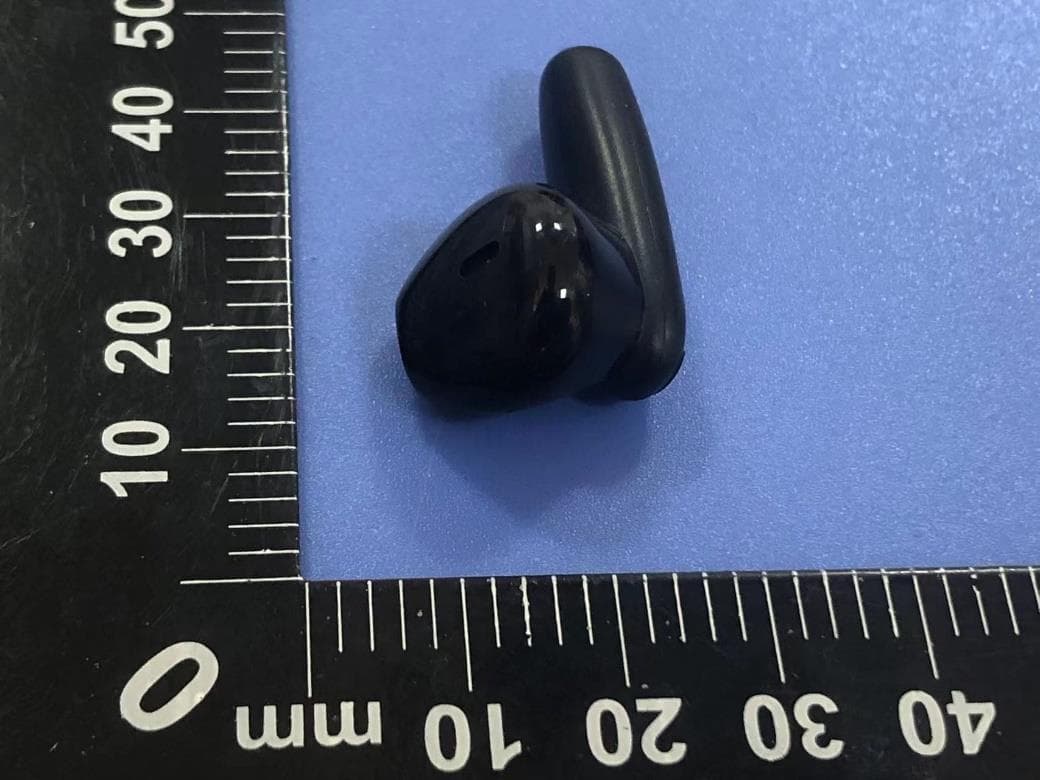
Click to zoom
Application Details
- Equipment Class
- DSS - Part 15 Spread Spectrum Transmitter
- Date of Grant
- Dec 12, 2023
- Application Purpose
- Original Equipment
- Date of Application
- Dec 11, 2023
- Equipment Note
- TWS-T19
- Frequency Range
- 2402.00000000 - 2480.00000000
- Country
- China
Documents & Files
Document Text
Text extracted from the exhibit documents filed with the FCC. Open a document above to read the original.
Users Manual
⁄›› ›ø ́ ̈∑±≤Ú Ã∏∑≠ ºª™∑Ωª Ω±≥∞¥∑ª≠ ©∑ ̈∏ ∞øÆ ̈ ÔÎ ±∫ ̈∏ª ⁄›› Œ ́¥ª≠Ú —∞ªÆø ̈∑±≤ ∑≠ ≠ ́æ∂ªΩ ̈ ̈± ̈∏ª ∫±¥¥±©∑≤π ̈©± Ω±≤º∑ ̈∑±≤≠Ê ̄Ô ̃ Ã∏∑≠ ºª™∑Ωª ≥øß ≤± ̈ Ωø ́≠ª ∏øÆ≥∫ ́¥ ∑≤ ̈ªÆ∫ªÆª≤ΩªÙ ø≤º ̄Ó ̃ ̈∏∑≠ ºª™∑Ωª ≥ ́≠ ̈ øΩΩª∞ ̈ ø≤ß ∑≤ ̈ªÆ∫ªÆª≤Ωª ÆªΩª∑™ªºÙ ∑≤Ω¥ ́º∑≤π ∑≤ ̈ªÆ∫ªÆª≤Ωª ̈∏ø ̈ ≥øß Ωø ́≠ª ́≤ºª≠∑ƪº ±∞ªÆø ̈∑±≤Ú fl≤ß ›∏ø≤πª≠ ±Æ ≥±º∑∫∑Ωø ̈∑±≤≠ ≤± ̈ ª®∞ƪ≠≠¥ß ø∞∞Ʊ™ªº æß ̈∏ª ∞øÆ ̈ß Æª≠∞±≤≠∑楪 ∫±Æ Ω±≥∞¥∑ø≤Ωª Ω± ́¥º ™±∑º ̈∏ª ́≠ªÆ ̆≠ ø ́ ̈∏±Æ∑ ̈ß ̈± ±∞ªÆø ̈ª ̈∏ª ªØ ́∑∞≥ª≤ ̈Ú “± ̈ªÊ Ã∏∑≠ ªØ ́∑∞≥ª≤ ̈ ∏ø≠ 檪≤ ̈ª≠ ̈ªº ø≤º ∫± ́≤º ̈± Ω±≥∞¥ß ©∑ ̈∏ ̈∏ª ¥∑≥∑ ̈≠ ∫±Æ ø ›¥ø≠≠ fi º∑π∑ ̈ø¥ ºª™∑ΩªÙ ∞ ́Æ≠ ́ø≤ ̈ ̈± ∞øÆ ̈ ÔÎ ±∫ ̈∏ª ⁄›› Œ ́¥ª≠Ú Ã∏ª≠ª ¥∑≥∑ ̈≠ øƪ ºª≠∑π≤ªº ̈± ∞Ʊ™∑ºª ƪø≠±≤ø楪 ∞Ʊ ̈ªΩ ̈∑±≤ øπø∑≤≠ ̈ ∏øÆ≥∫ ́¥ ∑≤ ̈ªÆ∫ªÆª≤Ωª ∑≤ ø ƪ≠∑ºª≤ ̈∑ø¥ ∑≤≠ ̈ø¥¥ø ̈∑±≤Ú Ã∏∑≠ ªØ ́∑∞≥ª≤ ̈ πª≤ªÆø ̈ª≠ ́≠ª≠ ø≤º Ωø≤ Æøº∑ø ̈ª Æøº∑± ∫ÆªØ ́ª≤Ωß ª≤ªÆπß ø≤ºÙ ∑∫ ≤± ̈ ∑≤≠ ̈ø¥¥ªº ø≤º ́≠ªº ∑≤ øΩΩ±Æºø≤Ωª ©∑ ̈∏ ̈∏ª ∑≤≠ ̈Æ ́Ω ̈∑±≤≠Ù ≥øß Ωø ́≠ª ∏øÆ≥∫ ́¥ ∑≤ ̈ªÆ∫ªÆª≤Ωª ̈± Æøº∑± Ω±≥≥ ́≤∑Ωø ̈∑±≤≠Ú ÿ±©ª™ªÆÙ ̈∏ªÆª ∑≠ ≤± π ́øÆø≤ ̈ªª ̈∏ø ̈ ∑≤ ̈ªÆ∫ªÆª≤Ωª ©∑¥¥ ≤± ̈ ±ΩΩ ́Æ ∑≤ ø ∞øÆ ̈∑Ω ́¥øÆ ∑≤≠ ̈ø¥¥ø ̈∑±≤Ú ◊∫ ̈∏∑≠ ªØ ́∑∞≥ª≤ ̈ º±ª≠ Ωø ́≠ª ∏øÆ≥∫ ́¥ ∑≤ ̈ªÆ∫ªÆª≤Ωª ̈± Æøº∑± ±Æ ̈ª¥ª™∑≠∑±≤ ÆªΩª∞ ̈∑±≤Ù ©∏∑Ω∏ Ωø≤ æª ºª ̈ªÆ≥∑≤ªº æß ̈ ́Æ≤∑≤π ̈∏ª ªØ ́∑∞≥ª≤ ̈ ±∫∫ ø≤º ±≤Ù ̈∏ª ́≠ªÆ ∑≠ ª≤Ω± ́Æø㦧 ̈± ̈Æß ̈± Ω±ÆÆªΩ ̈ ̈∏ª ∑≤ ̈ªÆ∫ªÆª≤Ωª æß ±≤ª ±Æ ≥±Æª ±∫ ̈∏ª ∫±¥¥±©∑≤π ≥ªø≠ ́ƪ≠Ê ÛŒª±Æ∑ª≤ ̈ ±Æ ƪ¥±Ωø ̈ª ̈∏ª ÆªΩª∑™∑≤π ø≤ ̈ª≤≤øÚ Û◊≤Ωƪø≠ª ̈∏ª ≠ª∞øÆø ̈∑±≤ æª ̈©ªª≤ ̈∏ª ªØ ́∑∞≥ª≤ ̈ ø≤º ÆªΩª∑™ªÆÚ Û›±≤≤ªΩ ̈ ̈∏ª ªØ ́∑∞≥ª≤ ̈ ∑≤ ̈± ø≤ ± ́ ̈¥ª ̈ ±≤ ø Ω∑ÆΩ ́∑ ̈ º∑∫∫ªÆª≤ ̈ ∫Ʊ≥ ̈∏ø ̈ ̈± ©∏∑Ω∏ ̈∏ª ÆªΩª∑™ªÆ ∑≠ Ω±≤≤ªΩ ̈ªºÚ Û›±≤≠ ́¥ ̈ ̈∏ª ºªø¥ªÆ ±Æ ø≤ ª®∞ªÆ∑ª≤Ωªº Æøº∑±Òà ̈ªΩ∏≤∑Ω∑ø≤ ∫±Æ ∏ª¥∞Ú Ã∏ª ºª™∑Ωª ∏ø≠ 檪≤ ª™ø¥ ́ø ̈ªº ̈± ≥ªª ̈ πª≤ªÆø¥ Œ⁄ ª®∞±≠ ́ƪ ÆªØ ́∑ƪ≥ª≤ ̈Ú Ã∏ª ºª™∑Ωª Ωø≤ æª ́≠ªº ∑≤ ∞±Æ ̈ø楪 ª®∞±≠ ́ƪ Ω±≤º∑ ̈∑±≤ ©∑ ̈∏± ́ ̈ ƪ≠ ̈Æ∑Ω ̈∑±≤Ú
Attestation Statements
Shenzhen Lanmi Electronics Co., Ltd Federal Communications Commission Authorization and Evaluation Division 7435 Oakland Mills Road Columbia, MD 21046 USA Date: 12/5/2023 FCC ID: 2BDTKT19 Ref. #1: Attestation Statements Part 2.911(d)(5)(i) Filing Shenzhen Lanmi Electronics Co., Ltd certifies that the equipment for which authorization is sought is not “covered” equipment prohibited from receiving an equipment authorization pursuant to section 2.903 of the FCC rules. Ref. #2: Attestation Statements Part 2.911(d)(5)(ii) Filing Shenzhen Lanmi Electronics Co., Ltd certifies that, as of the date of the filing of the application, the applicant is not identified on the Covered List as an entity producing “covered” equipment. Applicant: Shenzhen Lanmi Electronics Co., Ltd Address: 5th Floor, Building 9, Jinshun Industrial Park, Tongfu Road, Pingdi Street, Longgang District, Shenzhen Contact Person: Wu sixiao Tel.: 17665467582 Email: [email protected] Sincerely, Signature:
Attestation Statements
Effective Date: April 2, 2020 QSF 7.6.4-8 – Agent Authorization Letter Template Page 1 of 1 Revision Date: Revision: 0 Shenzhen Lanmi Electronics Co., Ltd Date:12/5/2023 Product Model Number: T19 FCC ID:2BDTKT19 To whom it may concern, Re: Product Certification Representative Authorization Letter We authorize QAI Laboratories Ltd. 3980 North Fraser Way, Burnaby B.C. Canada V5J 5K5 to act on our behalf on all matters concerning the above named equipment. This shall include the following: • Testing • Approval applications and procedures We declare that ORGANIZATION. is allowed to forward all information related to the approval project to the applied certification body and to the notification entities and to discuss any issues concerning the approval application. Any and all acts carried out by ORGANIZATION. on our behalf shall have the same effect as acts of our own. Signature: By: Wu sixiao Contact Listed on FCC Wesbite Title: Manger Email: [email protected] On behalf of: Shenzhen Lanmi Electronics Co., Ltd
Cover Letter(s)
Shenzhen Shenchao Communication Technology Co., Ltd Building 7, Tangxiayong Second Industrial Zone, Songgang Town, Bao'an District, Shenzhen Page 1 Version:1.0 Issue Date2023-9-8 Product specification CUSTOMER: 2.4G Antenna OUR MODEL NO: SPECIFICATIONS: 0 Q , TY: DATE: 2023-9-8 Shenzhen Shenchao Communication Technology Co., Ltd Building 7, Tangxiayong Second Industrial Zone, Songgang Town, Bao'an District, Shenzhen Page 2 Version:1.0 Issue Date2023-9-8 1. Technical Specification A. Electrical Characteristics Working Frequency Range 2400~2500MHz S.W.R. 2400~2500MHz:<3.0 Antenna Gain(Peak) 2400~2500MHz: 2.36dBi Type Chip Antenna Impedance 50ohm B. Material brass C. Environmental Operation Temperature -45°C~+85°C Storage Temperature -45°C~+85°C 2. Matching Circuits Element Value Vender E1(0402) OPEN / E2(0402) SHORT 50Ω E3(0402) OPEN / Shenzhen Shenchao Communication Technology Co., Ltd Building 7, Tangxiayong Second Industrial Zone, Songgang Town, Bao'an District, Shenzhen Page 3 Version:1.0 Issue Date2023-9-8 3. Curing antenna The parameter was performed using a Agilent 8753D Network Analyzer and BEST’S test fixture that was using customer-providing device. VSWR (Voltage standing wave ratio) The Voltage Standing Wave Ratio (VSWR) is an indication of how good the impedance match is. VSWR is often abbreviated as SWR. If the transmission line and the antenna are not matched, the antenna will not accept all the power from the transmission line. The part it does not accept is reflected back and forth between the transmitter and the antenna. This sets up a fixed wave pattern along the line which we can measure and which is called the voltage standing wave ration(VSWR).The VSWR (ratio of maximum voltage to the minimum voltage along the line)expresses the degree of match between the transmission line and the antenna. When the VSWR is 1 to 1(1:1) the match is perfect and all the energy is transferred to the antenna prior to be radiated. When the VSWR is 1.5:1, 96% of the power reaches the antenna. By definition VSWR can never be less than 1.VSWR and reflected power are different ways of measuring and expressing the same thing. A high VSWR is indication that the signal is reflected prior to being radiated by the antenna. VSWR Marker 2400MHz 2450MHz 2500MHz S.W.R <3.0 Shenzhen Shenchao Communication Technology Co., Ltd Building 7, Tangxiayong Second Industrial Zone, Songgang Town, Bao'an District, Shenzhen Page 4 Version:1.0 Issue Date2023-9-8 4. 3D 2400MHZ Gain:2.05dbi 2450MHZ Gain:2.36dbi 2500MHZ Gain:1.84dbi Shenzhen Shenchao Communication Technology Co., Ltd Building 7, Tangxiayong Second Industrial Zone, Songgang Town, Bao'an District, Shenzhen Page 5 Version:1.0 Issue Date2023-9-8 Frequency (MHz) Efficiency (%) Peak Gain / dB 2400 62.6 2.05 2450 65.7 2.36 2500 64.1 1.84 5. Product appearance diagram L W
Cover Letter(s)
Shenzhen Lanmi Electronics Co., Ltd Office of Engineering Technology Federal Communications Commission 7435 Oakland Mills Road Columbia, MD 21046 USA Date: December 6, 2023 Subject; Request for Confidentiality FCC ID: 2BDTKT19 To Whom It May Concern, Pursuant to the provisions of the Commission’s rules Title 47 Sections §0.457 and §0.459, we are requesting the Commission to withhold the following attachment(s) as confidential documents from public disclosure indefinitely. These documents contain detailed system and equipment descriptions and are considered as proprietary information in operation of the equipment. The public disclosure of these documents might be harmful to our company and would give competitors an unfair advantage in the market. Schematic Diagram Block Diagram Parts List Operational Description Tune-up Procedure In additional to above mentioned documents, in order to comply with the marketing regulations in Title 47 CFR §2.803 and the importation rules in Title 47 CFR §2.1204, while ensuring that business sensitive information remains confidential until the actual marketing of newly authorized devices, we request Short Term Confidentiality of the following attachment(s); External Photos Test Setup Photos Internal Photos User Manual For 45 days, pursuant to Public Notice DA 04-1705. OR For 180 days pursuant to KDB 726920 D01. It is our understanding that all measurement test reports, FCC ID label format and correspondence during the certification review process cannot be granted as confidential documents and this information will be available for public review once the grant of equipment authorization is issued. Sincerely, Signature: Name: Wu sixiao Title: Manger
External Photos
Page 1 of 10 Report No.: LGT23K063 Appendix - External Photographs of EUT Constructional Details Model: T19 Photo 1 Photo 2 Page 2 of 10 Report No.: LGT23K063 Photo 3 Photo 4 Page 3 of 10 Report No.: LGT23K063 Photo 5 Photo 6 Page 4 of 10 Report No.: LGT23K063 Photo 7 Photo 8 Page 5 of 10 Report No.: LGT23K063 Photo 9 Photo 10 Page 6 of 10 Report No.: LGT23K063 Photo 11 Photo 12 Page 7 of 10 Report No.: LGT23K063 Photo 13 Photo 14 Page 8 of 10 Report No.: LGT23K063 Photo 15 Photo 16 Page 9 of 10 Report No.: LGT23K063 Photo 17 Photo 18 Page 10 of 10 Report No.: LGT23K063 Photo 19 Photo 20
ID Label/Location Info
Label FCC ID: 2BDTKT19
Internal Photos
Page 1 of 5 Report No.: LGT23K063 Appendix - Internal Photographs of EUT Constructional Details Model: T19 Photo 1 Photo 2 Page 2 of 5 Report No.: LGT23K063 Photo 3 Photo 4 ANT Page 3 of 5 Report No.: LGT23K063 Photo 5 Photo 6 Page 4 of 5 Report No.: LGT23K063 Photo 7 Photo 8 ANT Page 5 of 5 Report No.: LGT23K063 Photo 9 Photo 10
Test Report
The test report is effective only with both signature and specialized stamp. This report shall not be reproduced except in full without the written approval of the Laboratory. The results in this report only apply to the tested sample. Shenzhen LGT Test Service Co., Ltd. Tel: 0755-89668180 E-mail:[email protected] Web: www.lgt-cert.com Room 205, Building 13, Zone B, Zhenxiong Industrial Park, No.177, Renmin West Road, Jinsha, Kengzi Street, Pingshan District, Shenzhen, Guangdong, China RF TEST REPORT Product Name: TWS-T19 Model Name: T19 FCC ID: 2BDTKT19 Issued For : Shenzhen Lanmi Electronics Co., Ltd 5th Floor, Building 9, Jinshun Industrial Park, Tongfu Road, Pingdi Street, Longgang District, Shenzhen Issued By : Shenzhen LGT Test Service Co., Ltd. Room 205, Building 13, Zone B, Zhenxiong Industrial Park, No.177, Renmin West Road, Jinsha, Kengzi Street, Pingshan District, Shenzhen, Guangdong, China Report Number: LGT23K063RF01 Sample Received Date: Nov. 17, 2023 Date of Test: Nov. 17, 2023 – Dec. 04, 2023 Date of Issue: Dec. 04, 2023 Report No.: LGT23K063RF01 Page 2 of 83 TEST REPORT CERTIFICATION Applicant: Shenzhen Lanmi Electronics Co., Ltd Address: 5th Floor, Building 9, Jinshun Industrial Park, Tongfu Road, Pingdi Street, Longgang District, Shenzhen Manufacturer: Shenzhen Lanmi Electronics Co., Ltd Address: 5th Floor, Building 9, Jinshun Industrial Park, Tongfu Road, Pingdi Street, Longgang District, Shenzhen Product Name: TWS-T19 Trademark: N/A Model Name: T19 Sample Status: Normal APPLICABLE STANDARDS STANDARD TEST RESULTS FCC Part 15.247, Subpart C ANSI C63.10-2013 PASS Prepared by: Approved by: Zane Shan Vita Li Engineer Technical Director Report No.: LGT23K063RF01 Page 3 of 83 Table of Contents Page 1. SUMMARY OF TEST RESULTS 6 1.1 TEST FACTORY 7 1.2 MEASUREMENT UNCERTAINTY 7 2. GENERAL INFORMATION 8 2.1 GENERAL DESCRIPTION OF THE EUT 8 2.2 DESCRIPTION OF THE TEST MODES 10 2.3 FREQUENCY HOPPING SYSTEM REQUIREMENTS 10 2.4 TABLE OF PARAMETERS OF TEST SOFTWARE SETTING 12 2.5 DESCRIPTION OF NECESSARY ACCESSORIES AND SUPPORT UNITS 12 2.6 EQUIPMENTS LIST 13 3. EMC EMISSION TEST 14 3.1 CONDUCTED EMISSION MEASUREMENT 14 3.2 RADIATED EMISSION MEASUREMENT 18 4. CONDUCTED SPURIOUS & BAND EDGE EMISSION 30 4.1 LIMIT 30 4.2 TEST PROCEDURE 30 4.3 TEST SETUP 31 4.4 EUT OPERATION CONDITIONS 31 4.5 TEST RESULTS 31 5. NUMBER OF HOPPING CHANNEL 32 5.1 LIMIT 32 5.2 TEST PROCEDURE 32 5.3 TEST SETUP 32 5.4 EUT OPERATION CONDITIONS 32 5.5 TEST RESULTS 32 6. AVERAGE TIME OF OCCUPANCY 33 6.1 LIMIT 33 6.2 TEST PROCEDURE 33 6.3 TEST SETUP 33 6.4 EUT OPERATION CONDITIONS 33 6.5 TEST RESULTS 33 7. HOPPING CHANNEL SEPARATION MEASUREMEN 34 7.1 LIMIT 34 7.2 TEST PROCEDURE 34 Report No.: LGT23K063RF01 Page 4 of 83 Table of Contents Page 7.3 TEST SETUP 34 7.4 EUT OPERATION CONDITIONS 34 7.5 TEST RESULTS 34 8. BANDWIDTH TEST 35 8.1 LIMIT 35 8.2 TEST PROCEDURE 35 8.3 TEST SETUP 35 8.4 EUT OPERATION CONDITIONS 35 8.5 TEST RESULTS 35 9. OUTPUT POWER TEST 36 9.1 LIMIT 36 9.2 TEST PROCEDURE 36 9.3 TEST SETUP 36 9.4 EUT OPERATION CONDITIONS 36 9.5 TEST RESULTS 36 10. ANTENNA REQUIREMENT 37 10.1 STANDARD REQUIREMENT 37 10.2 EUT ANTENNA 37 APPENDIX I:TEST RESULTS 38 DUTY CYCLE 38 MAXIMUM AVERAGE CONDUCTED OUTPUT POWER 42 MAXIMUM PEAK CONDUCTED OUTPUT POWER 46 -20DB BANDWIDTH 50 OCCUPIED CHANNEL BANDWIDTH 54 CARRIER FREQUENCIES SEPARATION 58 BAND EDGE 62 BAND EDGE(HOPPING) 67 CONDUCTED RF SPURIOUS EMISSION 72 NUMBER OF HOPPING CHANNEL 79 DWELL TIME 81 Report No.: LGT23K063RF01 Page 5 of 83 Revision History Rev. Issue Date Contents 00 Dec. 04, 2023 Initial Issue Report No.: LGT23K063RF01 Page 6 of 83 1. SUMMARY OF TEST RESULTS Test procedures according to the technical standards: KDB 558074 D01 15.247 Meas Guidance v05r02. FCC Part 15.247, Subpart C Standard Section Test Item Judgment Remark 15.207 Conducted Emission PASS -- 15.247(a)(1) Hopping Channel Separation PASS -- 15.247(a)(1)&(b)(1) Output Power PASS -- 15.209 Radiated Spurious Emission PASS -- 15.247(d) Conducted Spurious & Band Edge Emission PASS -- 15.247(a)(1)(iii) Number of Hopping Frequency PASS -- 15.247(a)(1)(iii) Dwell Time PASS -- 15.247(a)(1) Bandwidth PASS -- 15.205 Restricted bands of operation PASS -- Part 15.247(d)/part 15.209(a) Band Edge Emission PASS -- 15.203 Antenna Requirement PASS -- NOTE: (1) ‘N/A’ denotes test is not applicable in this Test Report. (2) All tests are according to ANSI C63.10-2013. Report No.: LGT23K063RF01 Page 7 of 83 1.1 TEST FACTORY Company Name: Shenzhen LGT Test Service Co., Ltd. Address: Room 205, Building 13, Zone B, Zhenxiong Industrial Park, No.177, Renmin West Road, Jinsha, Kengzi Street, Pingshan District, Shenzhen, Guangdong, China Accreditation Certificate A2LA Certificate No.: 6727.01 FCC Registration No.: 746540 CAB ID: CN0136 1.2 MEASUREMENT UNCERTAINTY The reported uncertainty of measurement y ± U, where expended uncertainty U is based on a standard uncertainty multiplied by a coverage factor of k=2, providing a level of confidence of approximately 95 %. No. Item Uncertainty 1 RF output power, conducted ±0.68dB 2 Unwanted Emissions, conducted ±2.988dB 3 All emissions, radiated 9K-30MHz ±2.84dB 4 All emissions, radiated 30M-1GHz ±4.39dB 5 All emissions, radiated 1G-6GHz ±5.10dB 6 All emissions, radiated>6G ±5.48dB 7 Conducted Emission (9KHz-150KHz) ±2.79dB 8 Conducted Emission (150KHz-30MHz) ±2.80dB Note: The measurement uncertainty is not included in the test result. Report No.: LGT23K063RF01 Page 8 of 83 2. GENERAL INFORMATION 2.1 GENERAL DESCRIPTION OF THE EUT Product Name: TWS-T19 Trademark: N/A Model Name: T19 Series Model: N/A Model Difference: N/A Channel List: Please refer to the Note 3. Bluetooth: Frequency:2402 – 2480 MHz Modulation: GFSK(1Mbps), π/4-DQPSK(2Mbps), 8DPSK(3Mbps) Antenna Type: Chip Antenna Gain: 2.36dBi Adapter: Input: DC 5V Battery: Rated Voltage: 3.7V Hardware Version: N/A Software Version: N/A Connecting I/O Port(s): Please refer to the Note 1. Note: 1. For a more detailed feature…
Text truncated - open the document above for the full version.
Test Setup Photos
Appendix Set-up for Radi Set-up for Radi Right Right Page 1 of 2 Report No.: ppendix - Test Setup photos Radiated Spurious Emission, Below 1GHz Radiated Spurious Emission, Above 1GHz Report No.: LGT23K063 Set Page 2 of 2 Report No.: Set-up for Conducted Emission Report No.: LGT23K063
Contact Information
Applicant
Wu sixiao(Manager)
Technical Contact
Test Firm
Shenzhen LGT Test Service Co., Ltd.Wen Wen
[email protected]0755-89668180
Technical Specifications
| # | Rule Parts | Frequency Range | Power Output |
|---|---|---|---|
| 1 | 15C | 2.40 GHz - 2.48 GHz | 3.77 mW |
Other Applications from Shenzhen Lanmi Electronics Co., Ltd
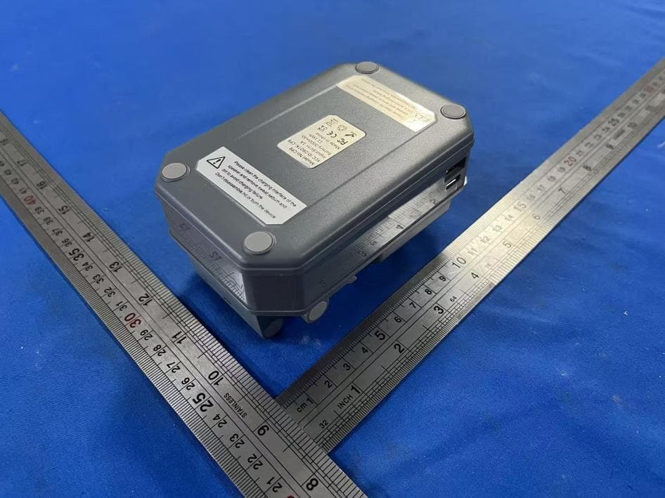
2BDTK-CP8
Nov 26, 2025Bluetooth speaker CP8
Equipment Class
DSS - Part 15 Spread Spectrum Transmitter