2BDZJ-K60wireless headphone
Dongguan Yande Electronic Technology Co., Ltd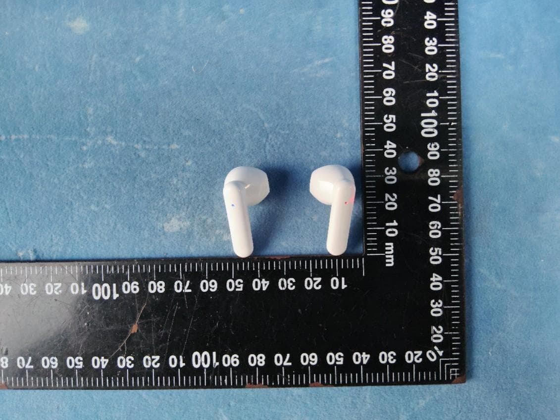
Click to zoom
Application Details
- Equipment Class
- DTS - Digital Transmission System
- Date of Grant
- Sep 29, 2024
- Application Purpose
- Original Equipment
- Date of Application
- Sep 29, 2024
- Equipment Note
- wireless headphone
- Frequency Range
- 2402.00000000 - 2480.00000000
- Country
- China
Documents & Files
Document Text
Text extracted from the exhibit documents filed with the FCC. Open a document above to read the original.
Users Manual
wireless headphone K60 Product parameters are laboratory test data, the specific data is subject to the use of data Product diagram Headset Configuration Charging bin configuration parameters .Pairs of ears connectedTwo-ear touch operation F&Q Matters needing attention Wearing a way Mode of operation 1. The boot 2.To turn it off Packing list Case material: ABS Charging time: about 1 hours Input voltage: 5V/ 500mAh Open the cover of the charging bin, take out the earphone of the right ear, and put the earphone horn end.Gently put into the ear canal of the right ear, and then gently swing the earphone not to shake.Wear the left earpiece in the same way. 1. Open the cover of the charging bin, take out the earphone and start it automatically. The red and blue lights are flashing, and we're in automatic formation mode, one of them headphones lights went out, said a team success. 2. Open the wireless list of the device and search for "K60". 3. Click "K60" to connect. If the connection fails, Put the earphones back on the cover of the charging bin. Put the lid on and repeat the top The operation procedure is ok. 4. Ears left connected to the equipment normal distance at the same time, Headset The headset is connected back to the wireless headset, and the connection is not completed with in 5 minutes If the connection is successful, both ears will shut down automatically. 5. Double-click after the headset is turned on and before the phone is disconnected Automatically switch between Chinese and English on either side of ears (Only Chinese or only English products do not have this function) After the device is connected for the first time, the next time the headset is restarted.It will automatically connect the last pair device (1) Open the cover of the charging bin, take out the earphone and turn it on Blue lights flashing (2) When the dryer is off, press the button for 3 seconds to start the machine (1) Put the earphone back to the charging bin, and the earphone will automatically shut down and charge (2) When the headset is on, press the button for 5 seconds to power off the headset Product Model: K60 Version: 5.3 Running time: about 5 hours Talk time: about 5 hours Operation mode: Touch control Charging time: about 1 hour Effective distance :≥10 m Horn: copper ring 8mm Play/pause the musicLight music condition according to the L/R headset under 1 1. Q: How come only one earphone has sound? A: Put the two earphones back into the charging bin at the same time, close the cover to charge, and then take them out to see whether the dual-ear mode is restored If the fault is not rectified, restore the fault to factory Settings 2. Q: The phone can' t connect to the headset? A: Delete the paired K60 on the mobile phone, and then make the paired connection. 3. Q: How can I listen to music/talk without sound? A: Android phones have a setting icon on the right side of the phone onnection record. Click enter to select two audi oDeselect and then re- select. Enter audio Call mode in Setting General Accessibility, and select Automatic, if it is automatic, then other options, and then change to automatic, if not restored, Delete the pairing record retry attempt. 4. Q: Why is there a stutter/ stutter? A: If . you use headphones, there are a lot of Wi- Fi devices, 4G signals, high power appliances and so onInterference, stuttering and di scontinuous condi tions may occur, and the connection can be restored by changing the environment or re- pairing. 。 1. Please use a charger with safety certification from a formal source for charging 2. Adjust the volume of headphones to avoid damage to hearing 3, the correct use of the product to avoid falling from high or heavy extrusion 4. Children should be accompanied by adults to avoid accidental ingestion 5. Stay away from extreme environments such as high temperature or humidity 6. Do not disassemble the product Play a songUnder the light press R headset 2 music condition Play the next songUnder the light press L headphones 2 music condition Light music, according to the 3 L volume plus +, light music condition according to the 3 R the volume - reduction Answer the phoneCalls, light according to the L/R headset under 1 Refuse to answer the phoneCalls, under the light according to the L/R headphones 2 (or long) Voice assistantNote 1.5 seconds long press any headphones let go nuclear state into speech aides Earphone charging: The earphone is automatically charged in the charging case The charging indicator light is red and the red light goes out when it is full Charging case low power: digital tube single digit flashing Charging case charging: digital tube single digit flashing, full 100 stop 1. Charging box *1 2. Left and right earphones *1 3. Product Manual *1 4. Charging cable *1 FCC Caution: This device complies with part 15 of the FCC Rules. Operation is subject to the following two conditions: (1) This device may not cause harmful interference, and (2) this device must accept any interference received, including interference that may cause undesired operation. Any changes or modifications not expressly approved by the party responsible for compliance could void the user's authority to operate the equipment.NOTE: This equipment has been tested and found to comply with the limits for a Class B digital device, pursuant to Part 15 of the FCC Rules. These limits are designed to provide reasonable protection against harmful interference in a residential installation. This equipment generates, uses and can radiate radio frequency energy and, if not installed and used in accordance with the instructions, may cause harmful interference to radio communications. However, there is no guarantee that interference will not occur in a particular installation.If this equipment does cause harmful interference to radio or television reception,which can be determined by turning the equipment off and on, the user is encouraged to try to correct the interference by one or more of the fol…
Text truncated - open the document above for the full version.
Attestation Statements
2.911(d)(5)(i)EquipmentTypeAttestationv1.2 DongguanYandeElectronicTechnologyCo.,Ltd Section2.911(d)(5)(i)Certification–EquipmentType Companyname:DongguanYandeElectronicTechnologyCo.,Ltd Address:Room508,Building3,No.19JinpengRoad,FenggangTown,Dongguan City,GuangdongProvince,China ProductName:wirelessheadphone FCCID:2BDZJ-K60 Model(s):K60 2.911(d)(5)(i)EquipmentType We,[DongguanYandeElectronicTechnologyCo.,Ltd]certifythattheequipmentforwhich authorizationissoughtthroughcertificationisnot: Prohibitedfromreceivinganequipmentauthorizationpursuantto§2.903;oftheFCCrules. Identifiedasanequipmenttypeinthe“CoveredList” NOTE1 Yourssincerely, Name:shiguanliangDate:09-27-2024 TitleandCompanyname:manager/DongguanYandeElectronicTechnologyCo.,Ltd NOTE1 “CoveredList”;istheListofEquipmentandServicesCoveredBySection2ofTheSecureNetworksAct,availableat https://www.fcc.gov/supplychain/coveredlist References; 1)986446D01CoveredEquipmentv01 https://apps.fcc.gov/oetcf/kdb/forms/FTSSearchResultPage.cfm?switch=P&id=325672 2)FederalRegisterdocument2022-28263publishedon02/06/23 https://www.federalregister.gov/documents/2023/02/06/2022-28263/protecting-against-national-security-threats-to-the-com munications-supply-chain-through-the
Attestation Statements
2.911(d)(5)(ii)ApplicantAttestationv1.3 DongguanYandeElectronicTechnologyCo.,Ltd Section2.911(d)(5)(ii)Certification–Applicant(CoveredList) Companyname:DongguanYandeElectronicTechnologyCo.,Ltd Address:Room508,Building3,No.19JinpengRoad,FenggangTown,Dongguan City,GuangdongProvince,China ProductName:wirelessheadphone FCCID:2BDZJ-K60 Model(s):K60 2.911(d)(5)(ii)Applicantfiling We,[DongguanYandeElectronicTechnologyCo.,Ltd]certifythat,asofthedateofthefilingof theapplication,theapplicantisnotidentified NOTE1 onthe“CoveredList” NOTE2 ,established pursuantto§1.50002ofthischapter,asanentityproducingcoveredcommunicationsequipment. Yourssincerely, Name:shiguanliangDate:09-27-2024 TitleandCompanyname:manager/DongguanYandeElectronicTechnologyCo.,Ltd NOTE1 Deleteoptionnotapplicabletothisapplication. NOTE2 “CoveredList”;istheListofEquipmentandServicesCoveredBySection2ofTheSecureNetworksAct,availableat https://www.fcc.gov/supplychain/coveredlist References; 1)986446D01CoveredEquipmentv01 https://apps.fcc.gov/oetcf/kdb/forms/FTSSearchResultPage.cfm?switch=P&id=325672 2)FederalRegisterdocument2022-28263publishedon02/06/23 https://www.federalregister.gov/documents/2023/02/06/2022-28263/protecting-against-national-security-threats-to-the-com munications-supply-chain-through-the
Attestation Statements
DongguanYandeElectronicTechnologyCo.,Ltd U.S.AgentLetterofAttestation To:FederalCommunicationsCommission 7435OaklandMillsRoad,Columbia,MD21046,USA Date:09-27-2024 Ref: AttestationStatement–Part 2.911(d)(7)filing FCCID:2BDZJ-K60 DongguanYandeElectronicTechnologyCo.,Ltdcertifiesthat,asofthedateofthefilingofthe application,THREESTONESMEDIALLCisourdesignatedU.S.agentforserviceofprocessfor theabovereferenceFCCID.Theapplicantacceptstomaintainanagentforserviceofprocessin theUnitedStatesfornolessthanoneyearaftereitherthegranteehaspermanentlyterminatedall marketingandimportationoftheapplicableequipmentwithintheU.S.,ortheconclusionofany Commission-relatedadministrativeorjudicialproceedinginvolvingtheequipment,whicheverislater. TheapplicantfurtheracknowledgesitisourresponsibilitytoinformtheFCCwhenevertheagent informationchanges. THREESTONESMEDIALLCunderstanditistheagent'sobligationtoacceptserviceofprocessin theUnitedStatesformattersrelatedtotheapplicableequipment,andatthephysicalU.S.address andemailaddress. DesignatedU.S.Agent CompanyName: THREESTONESMEDIALLC FRN:0033401761 GC:2A99E Address: 1200BroadwaySt.APT329,LosAngeles,CA90015 Signature: ContactPerson:SijieZhang Tel:+12679093692Email:[email protected] Applicant CompanyName:DongguanYandeElectronicTechnologyCo.,Ltd Address: Room508,Building3,No.19JinpengRoad, FenggangTown,DongguanCity,Guangdong Province,China Signature: ContactPerson:shiguanliang FRN:0034596106 GC:2BDZJ Email:[email protected]
Cover Letter(s)
DongguanYandeElectronicTechnologyCo.,Ltd OfficeofEngineeringTechnology FederalCommunicationsCommission 7435OaklandMillsRoad Columbia,MD21046 USA Date:09-27-2024 Subject;RequestforConfidentiality FCCID:2BDZJ-K60 ToWhomItMayConcern, PursuanttotheprovisionsoftheCommission’srulesTitle47Sections§0.457and§0.459,we arerequestingtheCommissiontowithholdthefollowingattachment(s)asconfidential documentsfrompublicdisclosureindefinitely. Thesedocumentscontaindetailedsystemandequipmentdescriptionsandareconsideredas proprietaryinformationinoperationoftheequipment.Thepublicdisclosureofthesedocuments mightbeharmfultoourcompanyandwouldgivecompetitorsanunfairadvantageinthemarket. SchematicDiagram BlockDiagram PartsList OperationalDescription Tune-upProcedure Inadditionaltoabovementioneddocuments,inordertocomplywiththemarketingregulations inTitle47CFR§2.803andtheimportationrulesinTitle47CFR§2.1204,whileensuringthat businesssensitiveinformationremainsconfidentialuntiltheactualmarketingofnewly authorizeddevices,werequestShortTermConfidentialityofthefollowingattachment(s); ExternalPhotos TestSetupPhotos InternalPhotos UserManual For45days,pursuanttoPublicNoticeDA04-1705. OR For180dayspursuanttoKDB726920D01. Itisourunderstandingthatallmeasurementtestreports,FCCIDlabelformatand correspondenceduringthecertificationreviewprocesscannotbegrantedasconfidential documentsandthisinformationwillbeavailableforpublicreviewoncethegrantofequipment authorizationisissued. Sincerely, Signature: Name:shiguanliang Title:manager
Cover Letter(s)
DongguanYandeElectronicTechnologyCo.,Ltd LetterofAuthorization Company:DongguanYandeElectronicTechnologyCo.,Ltd Address:Room508,Building3,No.19JinpengRoad,FenggangTown,Dongguan City,GuangdongProvince,China ProductName:wirelessheadphone ModelNumber(s):K60 ProductDescription:wirelessheadphone WeauthorizeMiCOMLabsInc.,575BoulderCourt,Pleasanton,California94566,USA, toactonourbehalfonallmattersconcerningthecertificationofabovenamed equipment. WedeclarethatMiCOMLabsInc.isallowedtoforwardallinformationrelatedtothe approvalandcertificationofequipmenttotheregulatoryagenciesasrequiredandto discussanyissuesconcerningtheapprovalapplication.Anyandallactscarriedoutby MiCOMLabsonourbehalfshallhavethesameeffectasactsofourown. Signature:Date:09-27-2024 Name:shiguanliang Title:manager Company:DongguanYandeElectronicTechnologyCo.,Ltd
External Photos
FCCID:2BDZJ-K60 FCCID:2BDZJ-K60 FCCID:2BDZJ-K60 FCCID:2BDZJ-K60
ID Label/Location Info
FCCID:2BDZJ-K60 Label Size:10mm*8mm FCCID:2BDZJ-K60 LabelLocation
Internal Photos
FCCID:2BDZJ-K60 FCCID:2BDZJ-K60 FCCID:2BDZJ-K60 ANT FCCID:2BDZJ-K60
RF Exposure Info
RFExposureevaluation FCCID2BDZJ-K60 ProductNamewirelessheadphone ModelNo.K60 ListedModel(s)-- ExposurecategoryGeneralpopulation/uncontrolledenvironment EUTTypeProductionUnit DeviceTypePortableDevice 1.Reference ANSIC95.1–1999:IEEEStandardforSafetyLevelswithRespecttoHumanExposureto RadioFrequencyElectromagneticFields,3kHzto300GHz. FCCKDBpublication447498D01GeneralRFExposureGuidancev06:MobileandPortable DevicesRFExposureProceduresandEquipmentAuthorizationPolicies. FCCCFR47part11.1310:Radiofrequencyradiationexposurelimits. FCCCFR47part22.1093:Radiofrequencyradiationexposureevaluation:portabledevices 2.Requirement AccordingtoKDB447498D01GeneralRFExposureGuidancev06Section4.3.1Standalone SARtestexclusionconsiderations:“UnlessspecificallyrequiredbythepublishedRFexposure KDBprocedures,standalone1-gheadorbodyand10-gextremitySARevaluationforgeneral populationexposureconditions,bymeasurementornumericalsimulation,isnotrequired whenthecorrespondingSARTestExclusionThresholdcondition,listedbelow,issatisfied. Thesetestexclusionconditionsarebasedonsource-basedtime-averagedmaximum conductedoutputpoweroftheRFchannelrequiringevaluation,adjustedfortune-uptolerance, andtheminimumtestseparationdistancerequiredfortheexposureconditions.22The minimumtestseparationdistanceisdeterminedbythesmallestdistancefromtheantenna andradiatingstructuresoroutersurfaceofthedevice,accordingtothehostformfactor, exposureconditionsandplatformrequirements,toanypartofthebodyorextremityofauser orbystander(see5)ofsection4.1).ToqualifyforSARtestexclusion,thetestseparation distancesappliedmustbefullyexplainedandjustifiedbytheoperatingconfigurationsand exposureconditionsofthetransmitterandapplicablehostplatformrequirements,typicallyin theSARmeasurementorSARanalysisreport,accordingtotherequiredpublishedRF exposureKDBprocedures.WhennootherRFexposuretestingorreportingisrequired,a statementofjustificationandcompliancemustbeincludedintheequipmentapproval,inlieuof theSARreport,toqualifyfortheSARtestexclusion.Whenrequired,thedevicespecific conditionsdescribedintheotherpublishedRFexposureKDBproceduresmustbesatisfied beforeapplyingtheseSARtestexclusionprovisions;forexample,handheldPTTtwo-way radios,handsets,laptops&tabletsetc.23” [(max.powerofchannel,includingtune-uptolerance,mW)/(min.testseparationdistance, mm)]·[√f(GHz)]≤3.0for1-gSARand≤7.5for10-gextremitySAR,where: •f(GHz)istheRFchanneltransmitfrequencyinGHz •PoweranddistanceareroundedtothenearestmWandmmbeforecalculation •Theresultisroundedtoonedecimalplaceforcomparison •3.0and7.5arereferredtoasthenumericthresholdsinthestep2below Thetestexclusionsareapplicableonlywhentheminimumtestseparationdistanceis≤50mm andfortransmissionfrequenciesbetween100MHzand6GHz.Whentheminimumtest separationdistanceis<5mm,adistanceof5mmaccordingto5)insection4.1isappliedto determineSARtestexclusion. Whenoneofthefollowingtestexclusionconditionsissatisfiedforallcombinationsof simultaneoustransmissionconfigurations,furtherequipmentapprovalisnotrequiredto incorporatetransmittermodulesinhostdevicesthatoperateinthemixedmobileandportable hostplatformexposureconditions.Thegranteeisresponsiblefordocumentingthisaccording toClassIpermissivechangerequirements.AntennasthatqualifyforstandaloneSARtest exclusionmustapplytheestimatedstandaloneSARtodeterminesimultaneoustransmission testexclusion. a)The[∑of(thehighestmeasuredorestimatedSARforeachstandaloneantenna configuration,adjustedformaximumtune-uptolerance)/1.6W/kg]+[∑ofMPEratios]is≤ 1.0. b)TheSARtopeaklocationseparationratiosofallsimultaneouslytransmittingantennapairs operatinginportabledeviceexposureconditionsareall≤0.04,andthe[∑ofMPEratios]is≤ 1.0. 3.ConductedPeakOutputPower ModulationPacketTypeChannel PeakOutput Power (dBm) PeakOutput Power (mW) GFSKBLE1M 05.113.24 194.742.98 394.122.58 GFSKBLE2M 05.163.28 195.013.17 394.422.76 4.ManufacturingTolerance BLE1M ChannelChannel0Channel19Channel39 Target(dBm)5.04.04.0 Tolerance±(dB)1.01.01.0 BLE2M ChannelChannel0Channel19Channel39 Target(dBm)5.05.04.0 Tolerance±(dB)1.01.01.0 5.EvaluationResult Band/Modef(GHz) Antenna Distance (mm) RFoutputpower SARTest Exclusion Threshold SARTest Exclusion dBmmW BLE2.40256 3.98 1.2340<3.0Yes Remark: 1.Outputpowerincludingtuneuptolerance; 2.Whentheminimumtestseparationdistanceis<5mm,adistanceof5mmaccordingtof)in section4.1isappliedtodetermineSARtestexclusion. 6.Conclusion ThemeasurementresultscomplywiththeFCCLimitper47CFR2.1093fortheuncontrolled RFExposureandSARExclusionThresholdperKDB447498D01V06. ------Endofthereport------
Test Report
2.4GHz2012ChipAntenna:RANT2012F245C07 Dimension(mm) L2.05+-0.10 W1.20+-0.10 T0.65+-0.10 No.TerminalName 1Feeding/GNG 2GND Application: WLAN,802.11b/g,Bluetooth,WLAN,etc... Features SMD,highreliability,ultraImpact,Omni-directional... PartnumberInformation RANT2012F245C07 (A)(B)(C)(D)(E)(F) (A)ProductTypeChipAntenna (B)SizeCode2.0x1.2mm(+-0.2mm) (C)MaterialHighKmaterial (D)Frequency2.4~2.5GHz (E)FeedingmodePIFA&SingleFeeding (F)AntennatypeType=07 ElectricalSpecification WorkingFrequencyRange2400 ~2500MHz Bandwidth84(Min.) PeakGain1.7dBi(Typ.) Impedance50Ohm Returnloss10dB(Min) PolarizationLinear AzimuthBeamwidthOmni-directional OperationTemperature( °C )-40~85 °C ResistancetoSolderingHeats 10sec.(@280°C) TerminationNi/Au(Leadless) ThespecificationisdefinedonEVB. DimensionandTerminalConfiguration ManufacturerRAIN International Technology Co., Ltd. 2.4GHz2012ChipAntenna:RANT2012F245C07 EvaluationBoardReference PCBDimensionAntennaLayoutReferenceUnit:mm ElectricalCharacteristics ReturnLoss ReturnLoss&Radiation 1 Frequency(MHz) S11(dB) 2400-10.77 2450-24.81 -10.2425003 Radiation Z Y X Test Setup 2.4GHz 2012 Chip Antenna: RANT2012F245C07 2.4GHz2012ChipAntenna:RANT2012F245C07 TapingSpecifications ReelandTapingSpecification ReelSpecification TYPESIZEABCD 20127”5K/Reel 9.0±0.5 60±213.5±0.5178±2 TappingSpecification PackagingTypeABWEFGHTDP PaperType2012 1.50±0.202.30±0.208.0±0.201.75±0.103.5±0.054.0±0.102.0±0.050.75±0.101.57±0.104.0±0.1 2.4GHz2012ChipAntenna:RANT2012F245C07 ReliabilityTable TestItemProcedure Requirements CeramicType Remark (Reference) Electrical Characterization Fulfilltheelectrical specification UserSpec. Thermal Shock 1.Preconditioning: 50±10°C/1hr,thenkeepfor24±1hrsatroomtemp. 2.Initialmeasure:Spec:referInitialspec. 3.Rapidchangeoftemperaturetest: -30°Cto+85°C;100cycles; 15minutesatLowercategorytemperature; 15minutesatUppercategorytemperature. NoVisibleDamage. Fulfilltheelectrical specification. MIL-STD-202 107 Temperature Cycling 1.Initialmeasure:Spec:referInitialspec. 2.100Cycles(-30°Cto+85°C),SoakMode=1(2Cycle/hours). 3.Measurementat24±2Hoursaftertestcondition. NoVisibleDamage. Fulfilltheelectrical specification. JESD22 JA104 HighTemperature Exposure 1.Initialmeasure:Spec:referInitialspec. 2.Unpowered;500hours@T=+85°C. 3.Measurementat24±2hoursaftertest. NoVisibleDamage. Fulfilltheelectrical specification. MIL-STD-202 108 LowTemperature Storage 1.Initialmeasure:Spec:referInitialspec. 2.Unpowered:500hours@T=-30°C. 3.Measurementat24±2hoursaftertest. NoVisibleDamage. Fulfilltheelectrical specification. MIL-STD-202 108 Solderability (SMDBottomSide) Dippingmethod: a.Temperature:235±5°C b.Dippingtime:3±0.5s Thesoldershouldcover over95%ofthecritical areaofbottomside. IEC60384-21/22 4.10 SolderingHeat Resistance (RSH) Preheatingtemperature:150±10°C. Preheatingtime:1~2min. Soldertemperature:260±5°C. Dippingtime:5±0.5s NoVisibleDamage.IEC60384-21/22 4.10 Vibration5g'sfor20min.,12cycleseachof3orientations Note:Use8"X5"PCB.031"thick7securepointson,onelong sideand2securepointsatcornersofoppositesides.Parts mountedwithin2"fromanysecurepoint.Testfrom10-2000 Hz. NoVisibleDamage.MIL-STD-202 Method204 Mechanical Shock Threeshocksineachdirectionshallbeappliedalongthethree mutuallyperpendicularaxesofthetestspecimen(18shocks) Peakvalue:1,500g’s Duration:0.5ms Velocitychange:15.4ft/s Waveform:Half-sine NoVisibleDamage.MIL-STD-202 Method213 Humidity Bias 1.Humidity:85%R.H.,Temperature:85±2°C. 2.Time:500±24hours. 3.Measurementat24±2hrsaftertestcondition. NoVisibleDamage. Fulfilltheelectrical specification. MIL-STD-202 Method106 2.4GHz2012ChipAntenna:RANT2012F245C07 2.4GHz2012ChipAntenna:RANT2012F245C07 _ Board Flex (SMD) 1.Mountingmethod: IR-Reflow.PCBSize(L:100×W:40×T:1.6mm) 2.Applytheloadindirectionofthearrowuntilbendingreaches 2mm. NoVisibleDamage.AEC-Q200 005 AdhesionForceof1.8Kgfor60seconds.NoVisibleDamage Magnificationof20Xor greatermaybeemployed forinspectionofthe mechanicalintegrityofthe devicebodyterminalsand body/terminaljunction. AEC-Q200 006 Physical Dimension Anyapplicablemethodusingx10magnification,micrometers, calipers,gauges,contourprojectors,orothermeasuring equipment,capableofdeterminingtheactualspecimen dimensions. Inaccordancewith specification. JESD22 JB100 RevisionHistory RevisionDateContent 12020/10/15NewDatasheet
Test Report
ReportNo.:CISRR240911100 —1— AppendixA ReportNo.: CISRR240911100 FCCID: 2BDZJ-K60 ProductName: wirelessheadphone ModelNo.:K60 TestEngineer:LucasHuang Supervisedby:RoryHuang ReportNo.:CISRR240911100 —2— 1)ConductedOutputPower TestResult ModeChannel PeakOutputPower (dBm) PeakOutputPower (mW) Limit (dBm) Result BLE1M 05.113.24≤30PASS 194.742.98≤30PASS 394.122.58≤30PASS BLE2M 05.163.28≤30PASS 195.013.17≤30PASS 394.422.76≤30PASS TestGraphs PeakOutputPower BLE1M_Channel0 PeakOutputPower BLE1M_Channel19 PeakOutputPower BLE1M_Channel39 PeakOutputPower BLE2M_Channel0 ReportNo.:CISRR240911100 —3— PeakOutputPower BLE2M_Channel19 PeakOutputPower BLE2M_Channel39 ReportNo.:CISRR240911100 —4— 2)99%Bandwidth TestResult ModeChannelCenterFrequency(MHz)99%BW(MHz) BLE1M024021.0306 BLE1M1924401.0346 BLE1M3924801.0314 BLE2M024022.0512 BLE2M1924402.0552 BLE2M3924802.0492 TestGraphs BLE1M_Channel0BLE2M_Channel0 BLE1M_Channel19BLE2M_Channel19 ReportNo.:CISRR240911100 —5— BLE1M_Channel39BLE2M_Channel39 ReportNo.:CISRR240911100 —6— 3)6dBBandwidth TestResult ModeChannel CenterFrequency (MHz) 6dBBandwidth (MHz) Limit (MHz) Result BLE1M 024020.6600 ≥0.5 PASS 1924400.6600PASS 3924800.6600PASS BLE2M 024021.150PASS 1924401.150PASS 3924801.160PASS TestGraphs BLE1M_Channel0BLE2M_Channel0 BLE1M_Channel19BLE2M_Channel19 ReportNo.:CISRR240911100 —7— BLE1M_Channel39BLE2M_Channel39 ReportNo.:CISRR240911100 —8— 4)ConductedOutOfBandEmission TestResult ModeChannel OOBEmission Frequency (MHz) OOBEmission Level (dBm) Limit (dBm) OverLimit (dB) Result BLE1M 0 2399.00-39.027-15.11-23.917PASS 2400.00-43.401-15.11-28.291PASS 7205.10-37.081-15.11-21.971PASS 199753.73-38.878-15.48-23.398PASS 39 2483.50-44.787-16.14-28.647PASS 9914.37-37.334-16.14-21.194PASS BLE2M 0 2400.00-30.226-15.22-15.006PASS 7204.30-40.489-15.22-25.269PASS 199753.73-38.927-15.44-23.487PASS 39 2483.50-48.808-16.01-32.798PASS 9914.37-36.930-16.01-20.920PASS TestGraphs In-BandReferenceLevel BLE1M_Channel0 In-BandReferenceLevel BLE2M_Channel0 OutOfBandEmissionOutOfBandEmission ReportNo.:CISRR240911100 —9— BLE1M_Channel0BLE2M_Channel0 30.0MHz-25000.0MHz BLE1M_Channel0 30.0MHz-25000.0MHz BLE2M_Channel0 In-BandReferenceLevel BLE1M_Channel19 In-BandReferenceLevel BLE2M_Channel19 30.0MHz-25000.0MHz BLE1M_Channel19 30.0MHz-25000.0MHz BLE2M_Channel19 ReportNo.:CISRR240911100 —10— In-BandReferenceLevel BLE1M_Channel39 In-BandReferenceLevel BLE2M_Channel39 OutOfBandEmission BLE1M_Channel39 OutOfBandEmission BLE2M_Channel39 30.0MHz-25000.0MHz BLE1M_Channel39 30.0MHz-25000.0MHz BLE2M_Channel39 ReportNo.:CISRR240911100 —11— 5)DutyCycle TestResult ModeChannelOnTime(ms)Period(ms)DutyCycle(%) DutyCycle (linear) DutyCycle Factor(dB) 1/T BLE1M 02.1342.50085.370.85370.68690.47 192.1342.49985.410.85410.6849 0.47 392.1332.49985.370.85370.6869 0.47 BLE2M 01.0822.50043.290.43293.63610.92 191.0812.49943.270.43273.63810.93 391.0812.49943.270.43273.63810.93 TestGraphs BLE1M_Channel0 ReportNo.:CISRR240911100 —12— BLE1M_Channel19 BLE1M_Channel39 ReportNo.:CISRR240911100 —13— BLE2M_Channel0 BLE2M_Channel19 ReportNo.:CISRR240911100 —14— BLE2M_Channel39 ReportNo.:CISRR240911100 —15— 6)PowerSpectralDensity TestResult ModeChannelPSD(dBm/3kHz)Limit(dBm/3kHz)Result BLE1M0-12.30≤8PASS BLE1M19-12.64≤8PASS BLE1M39-12.94≤8PASS BLE2M0-15.74≤8PASS BLE2M19-13.95≤8PASS BLE2M39-15.39≤8PASS TestGraphs BLE1M_Channel0BLE2M_Channel0 BLE1M_Channel19BLE2M_Channel19 ReportNo.:CISRR240911100 —16— BLE1M_Channel39BLE2M_Channel39
Test Report
ReportNo.:CISRR240911100 Page:1of27 TESTREPORT ReportNo.:CISRR240911100 ProjectNo.CISR240911100 FCCID2BDZJ-K60 Applicant:DongguanYandeElectronicTechnologyCo.,Ltd Address:Room508,Building3,No.19JinpengRoad,FenggangTown,Dongguan City,GuangdongProvince,China ManufacturerDongguanYandeElectronicTechnologyCo.,Ltd Address Room508,Building3,No.19JinpengRoad,FenggangTown,Dongguan City,GuangdongProvince,China ProductName:wirelessheadphone TradeMark:-- Model/Typereference:K60 ListedModel(s):-- Standard:Part15SubpartCSection15.247 Testdate:September12,2024~September19,2024 IssuedateSeptember20,2024 Testresult:Complied Preparedby:RoryHuangApprovedby:GenryLong Thetestresultsrelateonlytothetestedsamples. ThetestreportshouldnotbereproducedexceptinfullwithoutthewrittenapprovalofShenzhenBangce TestingTechnologyCo.,Ltd. ReportNo.:CISRR240911100 Page:2of27 Contents 1.REPORTVERSION.........................................................................................................................................3 2.SUMMARYOFTESTRESULT.......................................................................................................................4 3.SUMMARY.....................................................................................................................................................5 3.1.ProductDescription....................................................................................................................................5 3.2.RadioSpecificationDescription................................................................................................................5 3.3.ModificationofEUT.....................................................................................................................................6 3.4.TestingSite...................................................................................................................................................6 3.5.FieldStrengthCalculation..........................................................................................................................6 3.6.DISTURBANCECalculation........................................................................................................................6 4.TESTCONFIGURATION.............................................................................................................................7 4.1.Testfrequencylist.......................................................................................................................................7 4.2.Testmode.....................................................................................................................................................7 4.3.Supportunitusedintestconfigurationandsystem...............................................................................8 4.4.Testsampleinformation.............................................................................................................................8 4.5.Testingenvironmentalcondition...............................................................................................................8 4.6.Statementofthemeasurementuncertainty.............................................................................................8 4.7.EquipmentUsedduringtheTest...............................................................................................................9 5.TESTCONDITIONSANDRESULTS.....................................................................................................10 5.1.AntennaRequirement...............................................................................................................................10 5.2.ACConductedEmission...........................................................................................................................11 5.3.PeakOutputPower....................................................................................................................................14 5.4.6dBBandwidth..........................................................................................................................................15 5.5.99%OccupiedBandwidth.........................................................................................................................16 5.6.Powerspectraldensity..............................................................................................................................17 5.7.ConductedBandedgeandSpuriousEmission.....................................................................................18 5.8.RadiatedBandedgeEmission.................................................................................................................19 5.9.RadiatedSpuriousEmission....................................................................................................................21 5.10.DutyCycleCorrectionFactor(DCCF)...................................................................................................26 6.TESTSETUPPHOTOS............................................................................................................................27 7.EXTERNALANDINTERNALPHOTOSOFTHEEUT...........................................................…
Text truncated - open the document above for the full version.
Contact Information
Applicant
shiguan liang
Technical Contact
Test Firm
Shenzhen Bangce Testing Technology Co. , Ltd.Mike Jin Jin
[email protected]13824315318
Technical Specifications
| # | Rule Parts | Frequency Range | Power Output |
|---|---|---|---|
| 1 | 15C | 2.40 GHz - 2.48 GHz | 3.28 mW |
Other Applications from Dongguan Yande Electronic Technology Co., Ltd
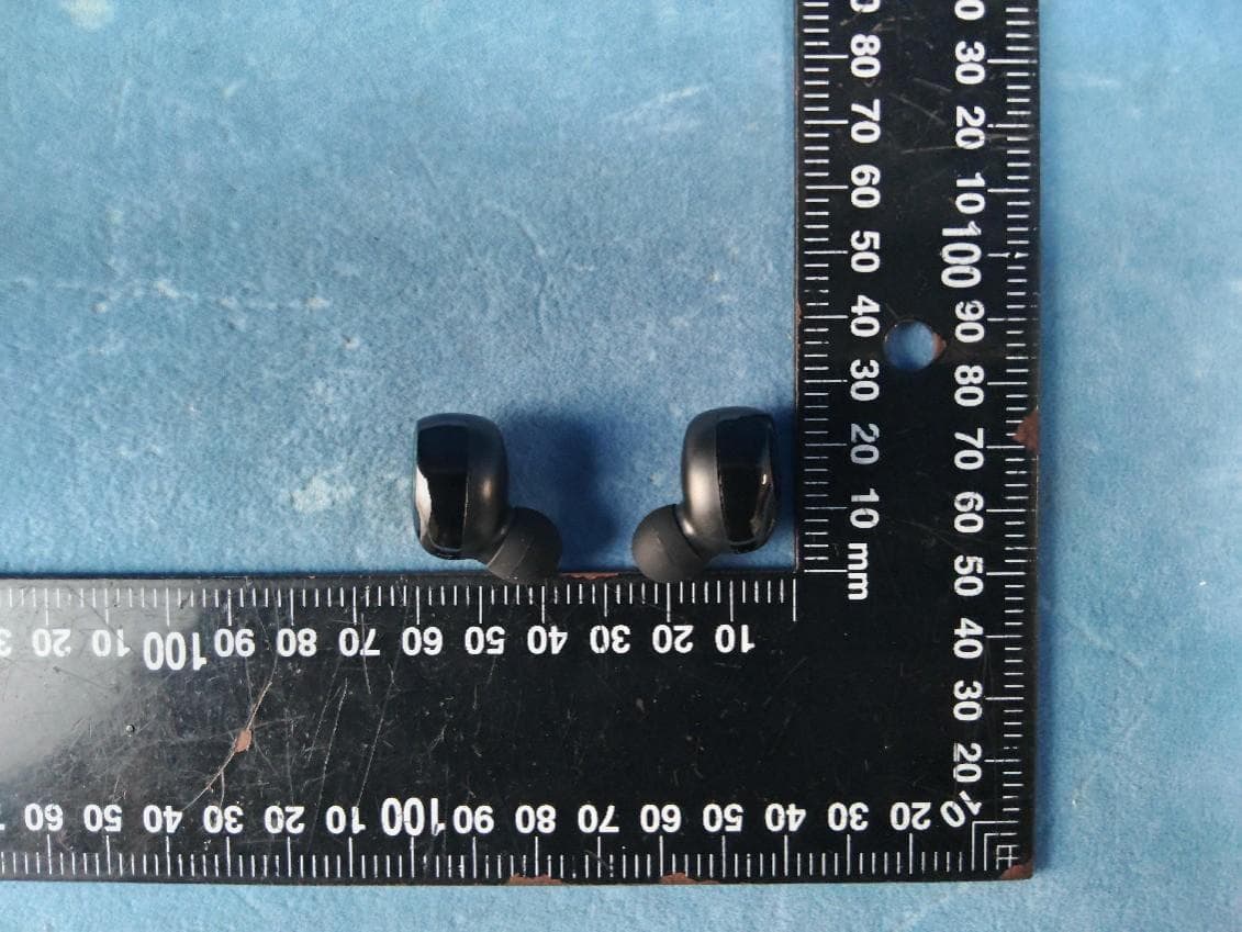
2BDZJ-BQ70
Sep 29, 2024wireless headphone
Equipment Class
DTS - Digital Transmission System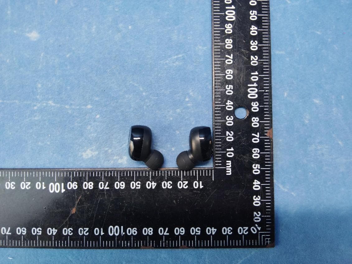
2BDZJ-BQ60
Sep 29, 2024wireless headphone
Equipment Class
DTS - Digital Transmission System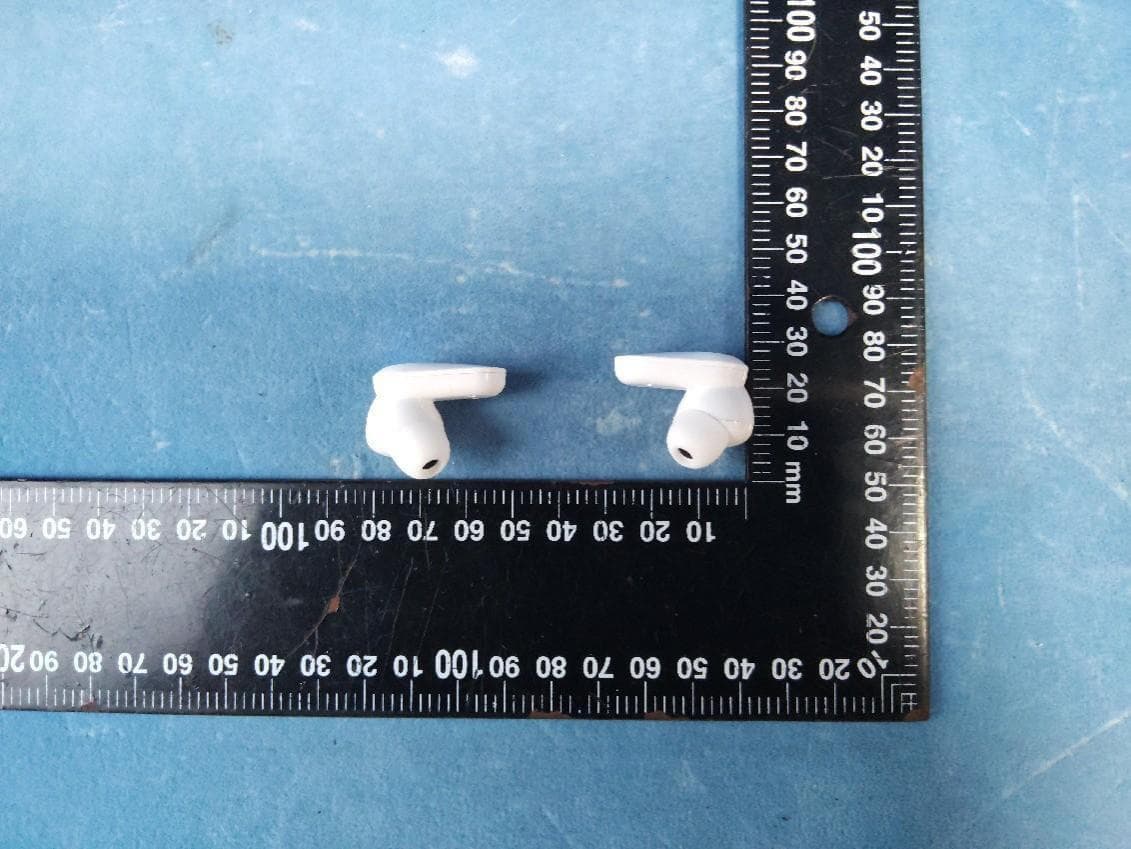
2BDZJ-YD08
Sep 29, 2024wireless headphone
Equipment Class
DTS - Digital Transmission System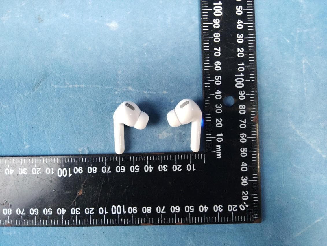
2BDZJ-VG121
Sep 29, 2024wireless headphone
Equipment Class
DTS - Digital Transmission System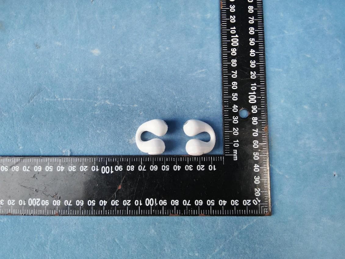
2BDZJ-JR01
Sep 28, 2024wireless headphone
Equipment Class
DTS - Digital Transmission System