2BE8V-AP300Key Finder
ShenZhen KaiFuTe Technology Co., Ltd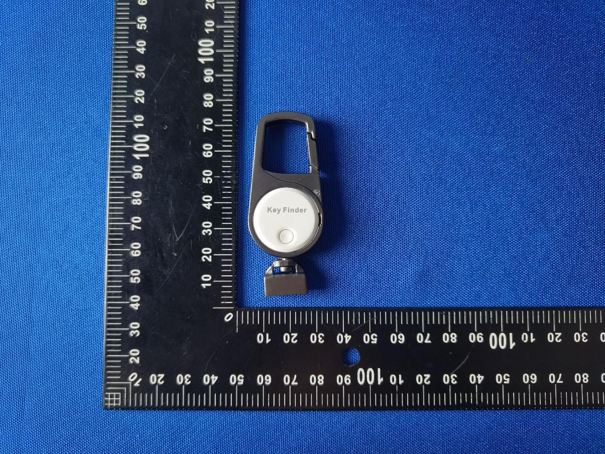
Click to zoom
Application Details
- Equipment Class
- DTS - Digital Transmission System
- Date of Grant
- Mar 17, 2024
- Application Purpose
- Original Equipment
- Date of Application
- Mar 17, 2024
- Equipment Note
- Key Finder
- Frequency Range
- 2402.00000000 - 2480.00000000
- Country
- China
Documents & Files
Document Text
Text extracted from the exhibit documents filed with the FCC. Open a document above to read the original.
Users Manual
FCC warning statements: This equipment has been tested and found to comply with the limits for a Class B digital device, pursuant to part 15 of the FCC Rules. These limits are designed to provide reasonable protection against harmful interference in a residential installation. This equipment generates, uses and can radiate radio frequency energy and, if not installed and used in accordance with the instructions, may cause harmful interference to radio communications. However, there is no guarantee that interference will not occur in a particular installation. If this equipment does cause harmful interference to radio or television reception, which can be determined by turning the equipment off and on, the user is encouraged to try to correct the interference by one or more of the following measures: • Reorient or relocate the receiving antenna. • Increase the separation between the equipment and receiver. • Connect the equipment into an outlet on a circuit different from that to which the receiver is connected. • Consult the dealer or an experienced radio/TV technician for help. Caution: Any changes or modifications to this device not explicitly approved by manufacturer could void your authority to operate this equipment. This device complies with part 15 of the FCC Rules. Operation is subject to the following two conditions: (1) This device may not cause harmful interference, and (2) this device must accept any interference received, including interference that may cause undesired operation. The device has been evaluated to meet general RF exposure requirement.
Attestation Statements
ShenZhen KaiFuTe Technology Co., Ltd. * the applicant must designate a contact located in the United States for purposes of acting as the applicant’s agent for service of process, regardless of whether the applicant is a domestic or foreign entity. An applicant located in the United States may designate itself as the agent for service of process. U.S. Agent Designation for Service of Process - Certification Attestation Letter 3/8/2024 ATTN.: Reviewing Engineer FCC ID: 2BE8V-AP300 FRN: 0035050475 Per section 2.911(d)(7) of the FCC rules, ShenZhen KaiFuTe Technology Co., Ltd. (“the applicant”) certifies that the equipment for which authorization is sought is designated to the following U.S. agent* for service of process: Company Name: JOC Australia Inc . FRN: 0033379421 Physical U.S. Company Address: CASTLETON ST STE 665, CITY OF INDUSTRY, CA 91748 United States of America Agent name: Benjamin. Smith/Vice President Agent Email Address: [email protected] Tel: +1 626 341 3408 The above contact person accepts the obligation for service of process. The applicant accepts to maintain an agent for no less than one year after the grantee has terminated all marketing and importation or the conclusion of any Commission-related proceeding involving the equipment. Applicant Signed: Signed: Printed name: Jim huang Title: general manager Company Name: ShenZhen KaiFuTe Technology Co., Ltd. Date: 3/8/2024 Agent Signed (if different to Applicant): Signed: Printed name: Benjamin. Smith Title: Vice President Company Name: JOC Australia Inc Date: 3/13/2024
Cover Letter(s)
ShenZhen KaiFuTe Technology Co., Ltd. 2024-03-07 Federal Communications Commission 7435 Oakland Mills Road Columbia, MD 21046 FCC ID: 2BE8V-AP300 Attn: Director of Certification Authority to Act as Agent On our behalf, I appoint Shenzhen Alpha Product Testing Co., Ltd. Address: Building i, No.2, Lixin Road, Fuyong Street, Bao’an District, 518103, Shenzhen, Guangdong, China Person: Mark Zhu (Name: Shenzhen Alpha Product Testing Co., Ltd. and address: Building i, No.2, Lixin Road, Fuyong Street, Bao’an District, 518103, Shenzhen, Guangdong, China). to act as our agent in the preparation of this application for equipment certification. I certify that submitted documents properly describe the device or system for which equipment certification is sought. I also certify that each unit manufactured, imported or marketed, as defined in the Federal Communications Commission’s regulations will have affixed to it a label identical to that submitted for approval with this application. For instances where our authorized agent signs the application for certification on our behalf, I acknowledge that all responsibility for complying with the terms and conditions for certification, as specified by TMICO still resides with ShenZhen KaiFuTe Technology Co., Ltd. Address: NO.201, Second Floor Hedi Maker Mashion, No. 28 Qingshui Road, Longxi Community Longgan District, Shenzhen City, China (applicant name and address). Signature: Name Jim huang Position general manager Company Name ShenZhen KaiFuTe Technology Co., Ltd. Address NO.201, Second Floor Hedi Maker Mashion, No. 28 Qingshui Road , Longxi Community Longgan District, Shenzhen City, China Tel 86-13923875848 Fax / Email [email protected]
Cover Letter(s)
ShenZhen KaiFuTe Technology Co., Ltd. Office of Engineering Technology Federal Communications Commission 7435 Oakland Mills Road Columbia, MD 21046 Date: March 7, 2024 Subject; Request for Long Term Confidentiality FCC ID: 2BE8V-AP300 To Whom It May Concern, Pursuant to the provisions of the Commission’s rules Title 47 Sections §0.457 and §0.459, we are requesting the Commission to withhold the following attachment(s) as confidential documents from public disclosure indefinitely. These documents contain detailed system and equipment descriptions and are considered as proprietary information in operation of the equipment. The public disclosure of these documents might be harmful to our company and would give competitors an unfair advantage in the market. Schematic Diagram Block Diagram Operational Description It is our understanding that all measurement test reports, FCC ID label format and correspondence during the certification review process cannot be granted as confidential documents and this information will be available for public review once the grant of equipment authorization is issued. Signature: Name Jim huang Position general manager Company Name ShenZhen KaiFuTe Technology Co., Ltd. Address NO.201, Second Floor Hedi Maker Mashion, No. 28 Qingshui Road , Longxi Community Longgan District, Shenzhen City, China Tel 86-13923875848 Fax / Email [email protected]
Cover Letter(s)
Differences Description We ShenZhen KaiFuTe Technology Co., Ltd. state: Product name: Key Finder Model: AP300, AP400 There is no difference except the appearance. All circuits, power supplies, and components are the same Signature: March 7, 2024 Name Jim huang Position general manager Company Name ShenZhen KaiFuTe Technology Co., Ltd. Address NO.201, Second Floor Hedi Maker Mashion, No. 28 Qingshui Road , Longxi Community Longgan District, Shenzhen City, China Tel 86-13923875848 Fax / Email [email protected]
External Photos
FCC ID: 2BE8V-AP300 FCC ID: 2BE8V-AP300 FCC ID: 2BE8V-AP300
Internal Photos
FCC ID: 2BE8V-AP300 FCC ID: 2BE8V-AP300 FCC ID: 2BE8V-AP300 FCC ID: 2BE8V-AP300 ANT
RF Exposure Info
FCC ID: 2BE8V-AP300 RF Exposure evaluation According to 447498 D01 General RF Exposure Guidance v06 The 1-g and 10-g SAR test exclusion thresholds for 100 MHz to 6 GHz at test separation distances ≤ 50 mm are determined by: [(max. power of channel, including tune-up tolerance, mW)/(min. test separation distance, mm)] ·[√f(GHz)] ≤ 3.0 for 1-g SAR and ≤ 7.5 for 10-g extremity SAR, where f(GHz) is the RF channel transmit frequency in GHz Power and distance are rounded to the nearest mW and mm before calculation The result is rounded to one decimal place for comparison Worse case is as below: [2402MHz: -0.619dBm (0.867mW) output power] (0.867mW /5mm)·[√2.402(GHz)]= 0.269<3.0 for 1-g SAR Then SAR evaluation is not required
Test Report
ALPHA's reports is using a digital certificate that is trusted on Adobe's official server. If there is no digital certificate or the digital certificate shows damaged in your report. Please do not accept the report. E-mail: [email protected] Tel: 4008-3008-95 Website: http://www.a-lab.cn FCC TEST REPORT FCC ID: 2BE8V-AP300 On Behalf of ShenZhen KaiFuTe Technology Co., Ltd. Key Finder Model No.: AP300, AP400 Prepared for : ShenZhen KaiFuTe Technology Co., Ltd. Address : NO.201, Second Floor Hedi Maker Mashion, No. 28 Qingshui Road, Longxi Community Longgan District, Shenzhen City, China Prepared By : Shenzhen Alpha Product Testing Co., Ltd. Address : Building i, No.2, Lixin Road, Fuyong Street, Bao’an District, 518103, Shenzhen, Guangdong, China Report Number : A2402064-C01-R05 Date of Receipt : February 23, 2024 Date of Test : February 23, 2024 - March 5, 2024 Date of Report : March 5, 2024 Version Number : V0 Result Pass Page 2 of 45 Report No.: A2402064-C01-R05 TABLE OF CONTENTS Description Page 1. Summary of Standards And Results -------------------------------------------------------------------------------- 5 1.1. Description of Standards and Results ------------------------------------------------------------------------ 5 2. General Information ------------------------------------------------------------------------------------------------------ 6 2.1. Description of Device (EUT) ------------------------------------------------------------------------------------ 6 2.2. Accessories of Device (EUT) ----------------------------------------------------------------------------------- 7 2.3. Tested Supporting System Details----------------------------------------------------------------------------- 7 2.4. Block Diagram of connection between EUT and simulators -------------------------------------------- 7 2.5. Test Mode Description -------------------------------------------------------------------------------------------- 7 2.6. Test Conditions ----------------------------------------------------------------------------------------------------- 8 2.7. Test Facility ---------------------------------------------------------------------------------------------------------- 8 2.8. Measurement Uncertainty --------------------------------------------------------------------------------------- 8 2.9. Test Equipment List ----------------------------------------------------------------------------------------------- 9 3. Spurious Emission ------------------------------------------------------------------------------------------------------- 10 3.1. Test Limits ---------------------------------------------------------------------------------------------------------- 10 3.2. Test Procedure ---------------------------------------------------------------------------------------------------- 10 3.3. Test Setup ---------------------------------------------------------------------------------------------------------- 11 3.4. Test Results -------------------------------------------------------------------------------------------------------- 12 4. Power Line Conducted Emission ----------------------------------------------------------------------------------- 23 4.1. Test Limits ---------------------------------------------------------------------------------------------------------- 23 4.2. Test Procedure ---------------------------------------------------------------------------------------------------- 23 4.3. Test Setup ---------------------------------------------------------------------------------------------------------- 23 4.4. Test Results -------------------------------------------------------------------------------------------------------- 23 5. Conducted Maximum peak Output Power------------------------------------------------------------------------ 24 5.1. Test limits ----------------------------------------------------------------------------------------------------------- 24 5.2. Test Procedure ---------------------------------------------------------------------------------------------------- 24 5.3. Test Setup ---------------------------------------------------------------------------------------------------------- 24 5.4. Test Results -------------------------------------------------------------------------------------------------------- 24 6. Peak Power Spectral Density ----------------------------------------------------------------------------------------- 25 6.1. Test limits ----------------------------------------------------------------------------------------------------------- 25 6.2. Test Procedure ---------------------------------------------------------------------------------------------------- 25 6.3. Test Setup ---------------------------------------------------------------------------------------------------------- 25 6.4. Test Results -------------------------------------------------------------------------------------------------------- 25 7. Bandwidth ------------------------------------------------------------------------------------------------------------------ 30 7.1. Test limits ----------------------------------------------------------------------------------------------------------- 30 7.2. Test Procedure ---------------------------------------------------------------------------------------------------- 30 7.3. Test Setup ---------------------------------------------------------------------------------------------------------- 30 7.4. Test Results -------------------------------------------------------------------------------------------------------- 30 8. Band Edge Check -------------------------------------------------------------------------------------------------------- 38 8.1. Test limits ----------------------------------------------------------------------------------------------------------- 38 8.2. Test Procedure ---------------------------------------------------------------------------------------------------- 38 8.3. Test Setup --------------…
Text truncated - open the document above for the full version.
Test Report
承 認 書 SPECIFICATION FOR APPROVAL 客戶名稱 CUSTOMER : 客戶料號 CUSTOMER’S P/N : 料號 PART NUMBER : WAN3216F245C0X 規格 DESCRIPTION : Chip Antenna 3216 L Ant 2.45G Type 02,04,06 版本 VERSION : V3.1 日期 ISSUE DATE : 2016/04/09 客 戶 承 認 CUSTOMER APPROVED 工 程 部 R&D CENTER 承 認 APPROVAL 確 認 CHECKED 製 作 DRAWN Ray James Thor 萬誠科技股份有限公司 OneWave Electronic Co., Ltd. 112台北市北投區中央南路二段36號3樓 2F., No.163, Sec. 1, Xi'an St., Beitou Dist., Taipei City 112, Taiwan 電話: (02) 2898-2220 TEL: +886 2 2898-2220 傳真: (02) 2898-5055 FAX: +886 2 2898-5055 2/11 ONEWAVE TECHNOLOGY CO., LTD. 3216 Chip antenna For Bluetooth / WLAN Applications Dimension (mm) L 3.23 ± 0.20 W 1.66 ± 0.20 T 0.45 ± 0.20 P/N: WAN3216F245C02 WAN3216F245C04 WAN3216F245C06 3/11 ONEWAVE TECHNOLOGY CO., LTD. Part Number Information WAN 3216 F 245 C 0X A B C D E F A Product Series Antenna B Dimension L x W 3.2X1.6mm (+-0.2mm) C Material High K material D Working Frequency 2.4 ~ 2.5GHz E Feeding mode PIFA & Single Feeding F Antenna type 0X=02,04,06 / Type=02,04,06 1. Electrical Specification Remark : Bandwidth & Peak Gain was measured under evaluation board of next page Specification Part Number WAN3216F245C02 WAN3216F245C04 WAN3216F245C06 Central Frequency 2450 MHz Bandwidth 120 (Min.) MHz Return Loss -6.5 (Max) dB Peak Gain 1.05 dBi Impedance 50 Ohm Operating Temperature -40~+85 °C Maximum Power 4 W Resistance to Soldering Heats 10 ( @ 260°C) sec. Polarization Linear Azimuth Beamwidth Omni-directional Termination Ni / Au (Leadless) 4/11 ONEWAVE TECHNOLOGY CO., LTD. 2. Recommended PCB Pattern Evaluation Board Dimension 2 nd Evaluation Board Dimension Suggested Matching Circuit 5/11 ONEWAVE TECHNOLOGY CO., LTD. Layout Dimensions in Clearance area( Size=4.40*5.0mm) FootPrint (Unit : mm) 2 nd Layout Dimensions in Clearance area( Size=8.0*3.0mm) Matching Circuit 50 ohm transmission Line 6/11 ONEWAVE TECHNOLOGY CO., LTD. 3. Measurement Results Return Loss 7/11 ONEWAVE TECHNOLOGY CO., LTD. Radiation Pattern Efficiency Peak Gain Directivity 2450MHz 76.65% 1.05 dBi 2.69 dBi Chamber Coordinate System X Y Z 8/11 ONEWAVE TECHNOLOGY CO., LTD. 4.Reliability and Test Condictions ITEM REQUIREMENTS TEST CONDITION Solderability 1. Wetting shall exceed 90% coverage 2. No visible mechanical damage Pre-heating temperature:150°C/60sec. Solder temperature:230±5°C Duration:4±1sec. Solder:Sn-Ag3.0-Cu0.5 Flux for lead free: rosin Solder heat Resistance 1. No visible mechanical damage 2. Central Freq. change :within ± 6% 10 ± 0.5 sec. 60 sec . . T E M P ( °C ) 150 °C 2 6 0 °C Pre-heating temperature:150°C/60sec. Solder temperature:260±5°C Duration:10±0.5sec. Solder:Sn-Ag3.0-Cu0.5 Flux for lead free: rosin Component Adhesion (Push test) 1. No visible mechanical damage The device should be reflow soldered(230±5°C for 10sec.) to a tinned copper substrate A dynometer force gauge should be applied the side of the component. The device must with-ST-F 0.5 Kg without failure of the termination attached to component. Component Adhesion (Pull test) 1. No visible mechanical damage Insert 10cm wire into the remaining open eye bend ,the ends of even wire lengths upward and wind together. Terminal shall not be remarkably damaged. Thermal shock 1. No visible mechanical damage 2. Central Freq. change :within ±6% Phase Temperature(°C) Time(min) 1 +85±5°C 30±3 2 Room Temperature Within 3sec 3 -40±2°C 30±3 4 Room Temperature Within 3sec +85°C=>30±3min -40°C=>30±3min Test cycle:10 cycles The chip shall be stabilized at normal condition for 2~3 hours before measuring. Resistance to High Temperature 1. No visible mechanical damage 2. Central Freq. change :within ±6% 3. No disconnection or short circuit. Temperature: 85±5°C Duration: 1000±12hrs The chip shall be stabilized at normal condition for 2~3 hours before measuring. Resistance to Low Temperature 1. No visible mechanical damage 2. Central Freq. change :within ±6% 3. No disconnection or short circuit. Temperature:-40±5°C Duration: 1000±12hrs The chip shall be stabilized at normal condition for 2~3 hours before measuring. Humidity 1. No visible mechanical damage 2. Central Freq. change :within ±6% 3. No disconnection or short circuit. Temperature: 40±2°C Humidity: 90% to 95% RH Duration: 1000±12hrs The chip shall be stabilized at normal condition for 2~3 hours before measuring. 4±1 sec. 60sec TEMP (°C) 150°C 230°C 9/11 ONEWAVE TECHNOLOGY CO., LTD. 5.Soldering and Mounting Mildly activated rosin fluxes are preferred. The minimum amount of solder can lead to damage from the stresses caused by the difference in coefficients of expansion between solder, chip and substrate. The terminations are suitable for all wave and re-flow soldering systems. If hand soldering cannot be avoided, the preferred technique is the utilization of hot air soldering tools. Recommended temperature profiles for re-flow soldering in Figure 1. Products attachment with a soldering iron is discouraged due to the inherent process control limitations. In the event that a soldering iron must be employed the following precautions are recommended. ‧Preheat circuit and products to 150°C ‧Never contact the ceramic with the iron tip ‧Use a 20 watt soldering iron with tip diameter of 1.0mm ‧280°C tip temperature (max) ‧1.0mm tip diameter (max) ‧Limit soldering time to 3 sec. SOLDERING COOLING NATURAL PRE-HEATING TEMPERATURE(°C) 60~120 s 10s max. 30~60s 250~260 230 180 150 TIME(sec.) Reflow Soldering SOLDERING COOLING NATURAL PRE-HEATING TEMPERATURE(°C) within 3s Gradual cooling 150 TIME(sec.) Iron Soldering Over 60s 350 300 10/11 ONEWAVE TECHNOLOGY CO., LTD. 6.Packaging Information Tape Specification: Reel Specification: (7’’, Φ180 mm) Tape Width(mm) A(mm) B(mm) C(mm) D(mm) Chip/Reel(pcs) 8 9.0±0.5 60±2 13.5±0.5 178±2 3000 11/11 ONEWAVE TECHNOLOGY CO., LTD. 7.Storage and Transportation Information Storage Conditions To maintain the solderability of terminal electrodes: 1. Temperature and humidity conditions: -10~ 40°C and 30~70% RH. 2. Recommended products should be used within 6 months from th…
Text truncated - open the document above for the full version.
Test Setup Photos
FCC ID: 2BE8V-AP300 Photo of Radiated Emission test FCC ID: 2BE8V-AP300 Photo of RF connect test FCC ID: 2BE8V-AP300
Contact Information
Applicant
Jim huang
Test Firm
Shenzhen Alpha Product Testing Co., LTD.Real Yak
[email protected]+86 755 29766001
Technical Specifications
| # | Rule Parts | Frequency Range | Power Output |
|---|---|---|---|
| 1 | 15C | 2.40 GHz - 2.48 GHz | 870.00 µW |
Other Applications from ShenZhen KaiFuTe Technology Co., Ltd
2BE8V-AS2059
Mar 17, 2024LCD expansion dock
Equipment Class
DTS - Digital Transmission System