2BGXI-WL-101Wireless microphone
FITSPARK USA INC.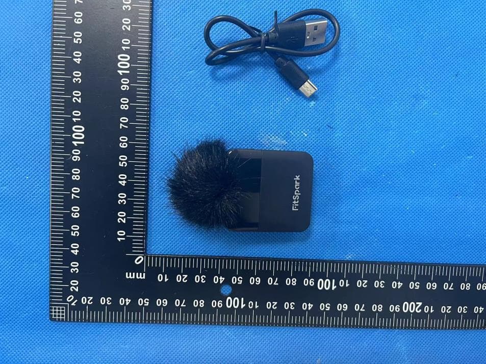
Click to zoom
Application Details
- Equipment Class
- DSS - Part 15 Spread Spectrum Transmitter
- Date of Grant
- Jul 21, 2024
- Application Purpose
- Original Equipment
- Date of Application
- Jul 21, 2024
- Equipment Note
- Wireless microphone
- Frequency Range
- 2402.00000000 - 2480.00000000
- Company
- FITSPARK USA INC.
- Country
- United States
Documents & Files
Document Text
Text extracted from the exhibit documents filed with the FCC. Open a document above to read the original.
Users Manual
尺寸: 105*80mm 105.00 mm CONTACT US Specifications are subject to change without prior notice. Please refer to the actual specifications! For any inquiries, questions or comments about our products, please send an email to [email protected]. We will reply as soon as possible. E E oo · o 00 r■ itSpc,rl( User Manual r■itSpc,rl( The Americas Asia FitSpark USA Inc. 30 N Gould St Ste R, Sheridan, WY 82801, USA FitSpark India Private Limited 135, 产Floor,Engineers Enclave, Pilampura, Delhi-110034, India Customer Care Email: [email protected] Website: https://www.myfitspark.com ©Copyright 2019-2024 FitSpark USA lnc./FitSpark India (P) Ltd. All rights reserved WIRELESS MIC 壳疗向三欣]砒@庞函归 Model: WL-101 范 Microphone Power indicator light Connected status light Mute light Charging indicator light Power button/ re pairing button Increase volume+/mute Decrease volume-/no,se reduction t r e 0 0 h- P gg en n .l g n.n o o r hit a p nh c Y c , 一 s 勹 』 B u e c Q du ht No 飞 g Fixed clip: The wireless microphone is fixed within 20cm of the emitting area, such as the collar of a garment. Microphone: Omni directional radio, DSP intelligent noise reduction. Power button: Long press power button 2 seconds to power on or off, the power indicator light will be light up when power on. Increase volume+: 1. Short press once to increase the volume 1 grid, there is 4 grid volume in total. When the volume reaches its maximum, there will be a prompt sound. 2. Long press to enter the mute mode, long press again to exit the mute mode. Decrease volume-: 1. Short press once to decrease the volume 1 grid, there is 4 grid volume 1n total. When the volume reaches its minimum, there will be a prompt sound. 2. Long press to enter the noise reduction mode, long press again to exit the noise reduction mode. Charging indicator: When it is low battery, the indicator light is flash with low battery prompt sound. The indicator light is light up when charging, once fully charge, the indicator light will light off. Connected status light: The pairing search status light flashes when turned on, and the light remains on for a long time when successfully connected to the receiver. Earphone monitoring hole : Plug in 3.5mm jack earphones (not included) to monitor audio recording effects in real-time. FCC Warning Statement Changes or modifications not expressly approved by the party responsible for compliance could void the user’s authority to operate the equipment. This equipment has been tested and found to comply with the limits for a Class B digital device, pursuant to Part 15 of the FCC Rules. These limits are designed to provide reasonable protection against harmful interference in a residential installation. This equipment generates uses and can radiate radio frequency energy and, if not installed and used in accordance with the instructions, may cause harmful interference to radio communications. However, there is no guarantee that interference will not occur in a particular installation. If this equipment does cause harmful interference to radio or television reception, which can be determined by turning the equipment off and on, the user is encouraged to try to correct the interference by one or more of the following measures: ‐‐ Reorient or relocate the receiving antenna. ‐‐ Increase the separation between the equipment and receiver. ‐‐ Connect the equipment into an outlet on a circuit different from that to which the receiver is connected. ‐‐ Consult the dealer or an experienced radio/TV technician for help. FCC Radiation Exposure Statement The device has been evaluated to meet general RF exposure requirement. The device can be used in portable exposure condition without restriction. This device complies with Part 15 of the FCC Rules. Operation is subject to the following two conditions: (1)This device may not cause harmful interference, and (2)This device must accept any interference received, including interference that may cause undesired operation.
Attestation Statements
Attestation Statements (2024/7/12) TO: Federal Communications Commission Authorization and Evaluation Division 7435 Oakland Mills Road Columbia, MD 21046, USA RE: Attestation Statements Part 2.911(d)(7) request for (FCC ID: 2BGXI-WL-101) (FITSPARK USA INC.), the undersigned, hereby authorize FITSPARK USA INC. to act as our designated U.S. agent for service of process, (FITSPARK USA INC.) accepts to maintain an agent for no less than one year after the grantee has terminated all marketing and importation or the conclusion of any Commission-related proceeding involving the equipment. FITSPARK USA INC. accepts the responsibility to act as designated U.S. agent for service of process. Applicant Information: Company Name: FITSPARK USA INC. Address: No.501, South China Development Center, No.1 South China Avenue, Pinghu, Longgang, Shenzhen, Guangdong, China Contact Name: Amol Gupta FRN: 0035548163 Telephone No: 001 307-217-4045 Email: [email protected] Signature [Amol Gupta] U.S. Agent Information: Company Name: FITSPARK USA INC. Address: No.501, South China Development Center, No.1 South China Avenue, Pinghu, Longgang, Shenzhen, Guangdong, China Contact Name: Amol Gupta FRN: 0035548163 Telephone No: 001 307-217-4045 Email: [email protected] Signature [Amol Gupta]
Attestation Statements
(FITSPARK USA INC.) (2024.7.12) Eurofins Electrical and Electronic Testing NA, Inc. 914 West Patapsco Avenue Baltimore, MD 21230 RE: Attestation Statements Part 2.911(d)(5)(i) request for (FCC ID: 2BGXI-WL-101) [FITSPARK USA INC.] (“the applicant”) certifies that the equipment for which authorization is sought is not “covered” equipment prohibited from receiving an equipment authorization pursuant to section 2.903 of the FCC rules. Sincerely, (Applicant signature) (Applicant printed name) Amol Gupta (FITSPARK USA INC.) (2024.7.12) Eurofins Electrical and Electronic Testing NA, Inc. 914 West Patapsco Avenue Baltimore, MD 21230 RE: Attestation Statements Part 2.911(d)(5)(ii) request for (FCC ID: 2BGXI-WL-101) [FITSPARK USA INC.] (“the applicant”) certifies that, as of the date of the filing of the application, the applicant is not identified on the Covered List as an entity producing “covered” equipment. Sincerely, (Applicant signature) (Applicant printed name) Amol Gupta
Block Diagram
FITSPARK USA INC. 2024.7.12 Eurofins Electrical and Electronic Testing NA, Inc. 914 W. Patapsco Avenue Baltimore, MD 21230 USA RE: CONFIDENTIALITY REQUEST FOR EUT NAME: Wireless microphone Trademark: FitSpark MODEL: WL-101 WL-102, WL-103, WL-104, WL-105, WL-106, WL-107, WL-108, WL-109, WL- 110 FCC ID: 2BGXI-WL-101 To Whom It May Concern: This letter serves as an official request for confidentiality under sections 0.457 and 0.459 of CFR 47. We have requested that the - Block Diagram - Schematics - Operational Description required to be submitted with this application be permanently withheld from public review. The above materials contain trade secrets and proprietary information not customarily released to the public. The public disclosure of these materials may be harmful to the applicant and provide unjustified benefits to its competitors. Please contact me if there is any information you may need. Sincerely, Client’s signature: Client’s name / title : Amol Gupta / Director Contact information / address: 30 N Gould St Ste R Sheridan, Wyoming 82801, United States
Cover Letter(s)
FITSPARK USA INC. 2024.7.12 Eurofins Electrical and Electronic Testing NA, Inc. 914 W. Patapsco Avenue Baltimore, MD 21230 USA RE: LETTER OF AGENT AUTHORIZATION To Whom It May Concern: We, the undersigned, hereby authorize Shenzhen BCTC Testing Co., Ltd to act on our behalf in all matters relating to application for equipment authorization, including the signing of all documents relating to these matters. We also hereby certify that no party to the application authorized hereunder is subject to the denial of benefits, including FCC benefits, pursuant to Section 5301 of the Anti-Drug Abuse Act of 1988, 21 U.S.C.853(a). This agreement expires one year from the current date. Sincerely, Client’s signature: Client’s name / title : Amol Gupta / Director Contact information / address: 30 N Gould St Ste R Sheridan, Wyoming 82801, United States
Cover Letter(s)
FITSPARK USA INC. Model Difference 2024/7/12 EUT NAME: Wireless microphone Trademark: FitSpark MODEL: WL-101 WL-102, WL-103, WL-104, WL-105, WL-106, WL-107, WL-108, WL-109, WL-110 FCC ID: 2BGXI-WL-101 All the models are the same circuit and RF module, except model names and appearance of the color. Regards Sincerely Client’s signature: Client’s name / title : Amol Gupta / Director Contact information / address: 30 N Gould St Ste R Sheridan, Wyoming 82801, United States
External Photos
External Photos
ID Label/Location Info
Label & label location Label: FCC ID: 2BGXI-WL-101
Internal Photos
Internal Photos Antenna
RF Exposure Info
RF EXPOSURE EVALUATION METHOD FCC ID: 2BGXI-WL-101 Applicable standard: In accordance with FCC 47 CFR part 2 (2.1093) this device has been defined as a portable device which is defined as a transmitting device designed to be used so that the radiating structure(s) of the device is/are within 20 centimeters of the body of the user. Portable devices must be evaluated using the specified in FCC 47 CFR part 2 (2.1093) and ANSI/IEEEC95.1-1992. and had been tested in accordance with the measurement methods and procedures specified in IEEE 1528-2003. Per FCC KDB 447498 D01 v06, the 1-g and 10-g SAR test exclusion thresholds for 100 MHz to 6 GHz at test separation distances s 50 mm are determined by: SAR Test Exclusion Thresholds for 100 MHz – 6 GHz and ≤ 50 mm Approximate SAR Test Exclusion Power Thresholds at Selected Frequencies and Test Separation Distances are illustrated in the following Table. The 1-g and 10-g SAR test exclusion thresholds for 100 MHz to 6 GHz at test separation distances ≤ 50 mm are determined by: [(max. power of channel, including tune-up tolerance, mW)/(min. test separation distance, mm)] · [√f(GHz)] ≤ 3.0 for 1-g SAR and ≤ 7.5 for 10-g extremity SAR,where f(GHz) is the RF channel transmit frequency in GHz Power and distance are rounded to the nearest mW and mm before calculation The result is rounded to one decimal place for comparison The test exclusions are applicable only when the minimum test separation distance is ≤ 50 mm and for transmission frequencies between 100 MHz and 6 GHz. When the minimum test separation distance is < 5 mm, a distance of 5 mm is applied to determine SAR test exclusion. BT Modulation Frequency Maximum Conducted Output Power(PK) Conducted Output Power Limit (MHz) (dBm) dBm GFSK 2402 -1.38 21 2441 -1.16 21 2480 -1.18 21 π/ 4 DQPSK 2402 -0.01 21 2441 0.23 21 2480 0.26 21 8DPSK 2402 0.11 21 2441 0.36 21 2480 0.34 21 max possible output power (PK,conducted):0±1dBm 1dBm=1.26mW 2402MHz [(max. power of channel, including tune-up tolerance, mW)/(min. test separation distance,mm)] · [√f(GHz)]= 1.26/5*√2.402=0.391≤3.0 2441MHz [(max. power of channel, including tune-up tolerance, mW)/(min. test separation distance,mm)] · [√f(GHz)]= 1.26/5*√2.441=0.394≤3.0 2480MHz [(max. power of channel, including tune-up tolerance, mW)/(min. test separation distance,mm)] · [√f(GHz)]= 1.26/5*√2.48=0.397≤3.0 Conclusion: 1. [(max. power of channel, including tune-up tolerance, mW)/(min. test separation distance, mm)] * [√f(GHz)] < 3.0. 2. SAR Test Exclusion Thresholds is 3.0 for separation distance 5mm. Therefore, SAR test is not required.
Test Report
2.4GHz Chip Antenna: YL5020H1R2G45 ______________________________________________________________________________________________________ Application: WLAN, 802.11b/g, Bluetooth, etc... Features SMD, high reliability, ultra Impact, Omni-directional... Electrical Specification Working Frequency Range 2400 ~2484 MHz Peak Gain 0.96dBi (Typ.) Impedance 50 Ohm Return loss 10 dB ( Min) Polarization Linear Azimuth Beamwidth Omni-directional Operation Temperature(°C) -40 ~85°C The specification is defined on EVB. Dimension and Terminal Configuration Part number YL 5020 H1 R 2G45 (1)(2)(3)(4) (5) (1)Product TypeChip Antenna (2) Size Code5.0x2.0mm (3) Type CodeH1 (4) PackingTape and reel (5) Frequency2.45GHz Dimension (mm) No. Terminal Name L 5.0 +-0.20 1 Feeding W 2.0+-0.20 2 Soldering T 0.60+-0.20 A 0.20+-0.20 永联无线 Manufacturer:Shenzhen Yonglian wireless Technology Co., LTD 2.4GHz 2.45HHz Chip Antenna:YL5020H1R2G45 ______________________________________________________________________________________________________ Evaluation Board Reference PCB Dimension & Antenna Layout Reference unit :mm Electrical Characteristics Return Loss & Radiation Return Loss Frequency (MHz) S11 (dB) 2400 -12.8 2442 -19.8 2484 -11.9 Radiation 2.45GHz Frequency 2445MHz Peak gain 0.96dBi Efficiency 80.2% 永联无线 2.4GHz 2.45HHz Chip Antenna: YL5020H1R2G45 ______________________________________________________________________________________________________ Taping Specifications Reel Taping Blister Tape Checking note Index Spec (mm) Internal diameter of reel A 60.20 ± 0.50 External diameter of reel B 178 ± 1.00 Quantity/per reel 3000 pcs Tape material Plastic (embossed) Checking note Index Spec (mm) Sprocket hole D0 1.50 +0.10/-0.00 Distance sprocket hole to outside E1 1.75 ± 0.10 Distance sprocket hole to pocket F 5.50 ± 0.05 Distance sprocket hole to sprocket hole P0 4.00 ± 0.10 Distance pocket to pocket P1 4.00 ± 0.10 Distance sprocket hole to pocket P2 2.00 ± 0.05 Tape width W 12.00 +0.30/-0.10 Pocket width nominal clearance A0 2.28 ± 0.13 Pocket length nominal clearance B0 5.70 ± 0.13 Pocket depth minimum clearance K0 1.58 ± 0.10 Thickness of tape T 0.23 ± 0.02 永联无线 2.4GHz 2.45HHz Chip Antenna: YL5020H1R2G45 ______________________________________________________________________________________________________ Reliability Table Test ItemProcedure Requirements Ceramic Type Remark (Reference) Electrical Characterization Fulfill the electrical specification User Spec. Thermal Shock 1. Preconditioning: 50 ± 10°C / 1 hr , then keep for 24 ± 1 hrs at room temp. 2. Initial measure: Spec: refer Initial spec. 3. Rapid change of temperature test: -30°C to +85°C; 100 cycles; 15 minutes at Lower category temperature; 15 minutes at Upper category temperature. No Visible Damage. Fulfill the electrical specification. MIL-STD-202 107 Temperature Cycling 1. Initial measure: Spec: refer Initial spec. 2. 100 Cycles (-30°C to +85°C), Soak Mode=1 (2 Cycle/hours). 3. Measurement at 24 ± 2Hours after test condition. No Visible Damage. Fulfill the electrical specification. JESD22 JA104 High Temperature Exposure 1. Initial measure: Spec: refer Initial spec. 2. Unpowered; 500hours @ T=+85°C. 3. Measurement at 24 ± 2 hours after test. No Visible Damage. Fulfill the electrical specification. MIL-STD-202 108 Low Temperature Storage 1. Initial measure: Spec: refer Initial spec. 2. Unpowered: 500hours @ T= -30°C. 3. Measurement at 24 ± 2 hours after test. No Visible Damage. Fulfill the electrical specification. MIL-STD-202 108 Solderability (SMD Bottom Side) Dipping method: a. Temperature: 235 ± 5°C b. Dipping time: 3 ± 0.5s The solder should cover over 95% of the critical area of bottom side. IEC 60384-21/22 4.10 Soldering Heat Resistance (RSH) Preheating temperature: 150 ± 10°C. Preheating time: 1~2 min. Solder temperature: 260 ± 5°C. Dipping time: 5 ± 0.5s No Visible Damage.IEC 60384-21/22 4.10 Vibration5g's for 20 min., 12 cycles each of 3 orientations Note: Use 8"X5" PCB .031" thick 7 secure points on, one long side and 2 secure points at corners of opposite sides. Parts mounted within 2" from any secure point. Test from 10-2000 Hz. No Visible Damage.MIL-STD-202 Method 204 Mechanical Shock Three shocks in each direction shall be applied along the three mutually perpendicular axes of the test specimen (18 shocks) Peak value: 1,500g’s Duration: 0.5ms Velocity change: 15.4 ft/s Waveform: Half-sine No Visible Damage.MIL-STD-202 Method 213 Humidity Bias 1. Humidity: 85% R.H., Temperature: 85 ± 2 °C. 2. Time: 500 ± 24 hours. 3. Measurement at 24 ± 2hrs after test condition. No Visible Damage. Fulfill the electrical specification. MIL-STD-202 Method 106 永联无线 2.4GHz 2.45HHz Chip Antenna: YL5020H1R2G45 ______________________________________________________________________________________________________ Revision History Revision Date Content 1 2019/7/20New issue Board Flex (SMD) 1. Mounting method: IR-Reflow. PCB Size (L:100 × W:40 × T:1.6mm) 2. Apply the load in direction of the arrow until bending reaches 2 mm. No Visible Damage.AEC-Q200 005 AdhesionForce of 1.8Kg for 60 seconds.No Visible Damage Magnification of 20X or greater may be employed for inspection of the mechanical integrity of the device body terminals and body/terminal junction. AEC-Q200 006 Physical Dimension Any applicable method using x10 magnification, micrometers, calipers, gauges, contour projectors, or other measuring equipment, capable of determining the actual specimen dimensions. In accordance with specification. JESD22 JB100 永联无线
Test Report
No.:BCTC/RF-EMC-005 Page: 1 of 84 Edition:B.2 TEST REPORT Shenzhen BCTC Testing Co., Ltd. Report No.: BCTC2406243243E Applicant: FITSPARK USA INC. Product Name: Wireless microphone Test Model: WL-101 Tested Date: 2024-06-12 to 2024-06-24 Issued Date: 2024-06-24 Report No.:BCTC2406243243E No.:BCTC/RF-EMC-005 Page: 2 of 84 Edition:B.2 FCC ID: 2BGXI-WL-101 The test report is effective only with both signature and specialized stamp. This result(s) shown in this report refer only to the sample(s) tested. Without written approval of Shenzhen BCTC Testing Co., Ltd, this report can’t be reproduced except in full. The tested sample(s) and the sample information are provided by the client. Product Name: Wireless microphone Trademark: FitSpark Model/Type Reference: WL-101 WL-102, WL-103, WL-104, WL-105, WL-106, WL-107, WL-108, WL-109, WL-110 Prepared For: FITSPARK USA INC. Address: 30 N Gould St Ste R Sheridan, Wyoming 82801, United States Manufacturer: TRANSTYLE TECHNOLOGY CO., LIMITED Address: Room 404, Gainian Kongjian Factory, Building B, No.32 Huimin 1st Road, Guihua community, Guanlan Street, Longhua District, Shenzhen City, China. Prepared By: Shenzhen BCTC Testing Co., Ltd. Address: 1-2/F., Building B, Pengzhou Industrial Park, No.158, Fuyuan 1st Road, Zhancheng, Fuhai Subdistrict, Bao'an District, Shenzhen, Guangdong, China Sample Received Date: 2024-06-12 Sample tested Date: 2024-06-12 to 2024-06-24 Issue Date: 2024-06-24 Report No.: BCTC2406243243E Test Standards FCC Part15.247 ANSI C63.10-2013 Test Results PASS Remark: This is Bluetooth Classic radio test report. Tested by: Approved by: Shanshan. Zhang / Project Handler Zero Zhou/Reviewer Report No.:BCTC2406243243E No.:BCTC/RF-EMC-005 Page: 3 of 84 Edition:B.2 Table Of Content Test Report Declaration Page 1. Version .................................................................................................................. 5 2. Test Summary ....................................................................................................... 6 3. Measurement Uncertainty ..................................................................................... 7 4. Product Information And Test Setup ..................................................................... 8 4.1 Product Information ............................................................................................... 8 4.2 Test Setup Configuration ...................................................................................... 8 4.3 Support Equipment ............................................................................................... 9 4.4 Channel List .......................................................................................................... 9 4.5 Test Mode ........................................................................................................... 10 4.6 Table Of Parameters Of Text Software Setting ................................................... 10 5. Test Facility And Test Instrument Used ............................................................... 11 5.1 Test Facility ......................................................................................................... 11 5.2 Test Instrument Used .......................................................................................... 11 6. Conducted Emissions .......................................................................................... 13 6.1 Block Diagram Of Test Setup .............................................................................. 13 6.2 Limit .................................................................................................................... 13 6.3 Test procedure .................................................................................................... 13 6.4 EUT operating Conditions ................................................................................... 13 6.5 Test Result .......................................................................................................... 14 7. Radiated emissions ............................................................................................. 16 7.1 Block Diagram Of Test Setup .............................................................................. 16 7.2 Limit .................................................................................................................... 17 7.3 Test procedure .................................................................................................... 18 7.4 EUT operating Conditions ................................................................................... 19 7.5 Test Result .......................................................................................................... 19 8. Radiated Band Emission Measurement And Restricted Bands Of Operation ..... 23 8.1 Block Diagram Of Test Setup .............................................................................. 23 8.2 Limit .................................................................................................................... 23 8.3 Test procedure .................................................................................................... 24 8.4 EUT operating Conditions ................................................................................... 24 8.5 Test Result .......................................................................................................... 25 9. Spurious RF Conducted Emissions ..................................................................... 26 9.1 Block Diagram Of Test Setup .............................................................................. 26 9.2 Limit .................................................................................................................... 26 9.3 Test procedure .................................................................................................... 26 9.4 Test Result .................................…
Text truncated - open the document above for the full version.
Test Report
Report No.:BCTC2406243243E No.:BCTC/RF-EMC-005 Page: 46 of 84 Edition:B.2 Band Edge(Hopping) NVNT 3-DH1 2402MHz Hopping Band Edge(Hopping) NVNT 3-DH1 2402MHz Hopping Emission Report No.:BCTC2406243243E No.:BCTC/RF-EMC-005 Page: 47 of 84 Edition:B.2 Band Edge(Hopping) NVNT 3-DH1 2480MHz Hopping Band Edge(Hopping) NVNT 3-DH1 2480MHz Hopping Emission Report No.:BCTC2406243243E No.:BCTC/RF-EMC-005 Page: 48 of 84 Edition:B.2 10. 20 dB Bandwidth 10.1 Block Diagram Of Test Setup 10.2 Limit N/A 10.3 Test procedure 1. Set RBW = 30kHz. 2. Set the video bandwidth (VBW) ≥ 3 x RBW. 3. Detector = Peak. 4. Trace mode = max hold. 5. Sweep = auto couple. 6. Allow the trace to stabilize. 7. Measure the maximum width of the emission that is constrained by the frequencies associated with the two outermost amplitude points (upper and lower frequencies) that are attenuated by 6 dB relative to the maximum level measured in the fundamental emission. 10.4 Test Result Temperature: 26°C Relative Humidity: 54% Test Voltage: DC 3.7V Remark: N/A Condition Mode Frequency (MHz) -20 dB Bandwidth (MHz) Verdict NVNT 1-DH1 2402 0.691 Pass NVNT 1-DH1 2441 0.752 Pass NVNT 1-DH1 2480 0.741 Pass NVNT 2-DH1 2402 1.108 Pass NVNT 2-DH1 2441 1.135 Pass NVNT 2-DH1 2480 1.137 Pass NVNT 3-DH1 2402 1.101 Pass NVNT 3-DH1 2441 1.084 Pass NVNT 3-DH1 2480 1.098 Pass Report No.:BCTC2406243243E No.:BCTC/RF-EMC-005 Page: 49 of 84 Edition:B.2 Test Graphs -20dB Bandwidth NVNT 1-DH1 2402MHz -20dB Bandwidth NVNT 1-DH1 2441MHz Report No.:BCTC2406243243E No.:BCTC/RF-EMC-005 Page: 50 of 84 Edition:B.2 -20dB Bandwidth NVNT 1-DH1 2480MHz -20dB Bandwidth NVNT 2-DH1 2402MHz Report No.:BCTC2406243243E No.:BCTC/RF-EMC-005 Page: 51 of 84 Edition:B.2 -20dB Bandwidth NVNT 2-DH1 2441MHz -20dB Bandwidth NVNT 2-DH1 2480MHz Report No.:BCTC2406243243E No.:BCTC/RF-EMC-005 Page: 52 of 84 Edition:B.2 -20dB Bandwidth NVNT 3-DH1 2402MHz -20dB Bandwidth NVNT 3-DH1 2441MHz Report No.:BCTC2406243243E No.:BCTC/RF-EMC-005 Page: 53 of 84 Edition:B.2 -20dB Bandwidth NVNT 3-DH1 2480MHz Report No.:BCTC2406243243E No.:BCTC/RF-EMC-005 Page: 54 of 84 Edition:B.2 11. Maximum Peak Output Power 11.1 Block Diagram Of Test Setup 11.2 Limit FCC Part15 (15.247) , Subpart C Section Test Item Limit Frequency Range (MHz) Result 15.247(b)(1) Peak Output Power 0.125 watt or 21dBm 2400-2483.5 PASS 11.3 Test procedure 1. Remove the antenna from the EUT and then connect a low RF cable from the antenna port to the spectrum. 2. Set the spectrum analyzer: RBW = 2MHz. VBW = 6MHz. Sweep = auto; Detector Function = Peak. 3. Keep the EUT in transmitting at lowest, medium and highest channel individually. Record the max value. 11.4 Test Result Temperature: 26°C Relative Humidity: 54% Test Voltage: DC 3.7V Remark: N/A Condition Mode Frequency (MHz) Conducted Power (dBm) Limit (dBm) Verdict NVNT 1-DH1 2402 -1.38 21 Pass NVNT 1-DH1 2441 -1.16 21 Pass NVNT 1-DH1 2480 -1.18 21 Pass NVNT 2-DH1 2402 -0.01 21 Pass NVNT 2-DH1 2441 0.23 21 Pass NVNT 2-DH1 2480 0.26 21 Pass NVNT 3-DH1 2402 0.11 21 Pass NVNT 3-DH1 2441 0.36 21 Pass NVNT 3-DH1 2480 0.34 21 Pass Report No.:BCTC2406243243E No.:BCTC/RF-EMC-005 Page: 55 of 84 Edition:B.2 Test Graphs Power NVNT 1-DH1 2402MHz Power NVNT 1-DH1 2441MHz Report No.:BCTC2406243243E No.:BCTC/RF-EMC-005 Page: 56 of 84 Edition:B.2 Power NVNT 1-DH1 2480MHz Power NVNT 2-DH1 2402MHz Report No.:BCTC2406243243E No.:BCTC/RF-EMC-005 Page: 57 of 84 Edition:B.2 Power NVNT 2-DH1 2441MHz Power NVNT 2-DH1 2480MHz Report No.:BCTC2406243243E No.:BCTC/RF-EMC-005 Page: 58 of 84 Edition:B.2 Power NVNT 3-DH1 2402MHz Power NVNT 3-DH1 2441MHz Report No.:BCTC2406243243E No.:BCTC/RF-EMC-005 Page: 59 of 84 Edition:B.2 Power NVNT 3-DH1 2480MHz Report No.:BCTC2406243243E No.:BCTC/RF-EMC-005 Page: 60 of 84 Edition:B.2 12. Hopping Channel Separation 12.1 Block Diagram Of Test Setup 12.2 Limit Frequency hopping systems shall have hopping channel carrier frequencies separated by a minimum of 25 kHz or the 20 dB bandwidth of the hopping channel, whichever is greater. Alternatively, frequency hopping systems operating in the 2400-2483.5 MHz band may have hopping channel carrier frequencies that are separated by 25 kHz or two-thirds of the 20 dB bandwidth of the hopping channel, whichever is greater, provided the systems operate with an output power no greater than 0.125W. 12.3 Test procedure 1. Remove the antenna from the EUT and then connect a low RF cable from the antenna port to the spectrum. 2. Set the spectrum analyzer: RBW = 30kHz. VBW = 100kHz , Span = 2.0MHz. Sweep = auto; Detector Function = Peak. Trace = Max hold. 3. Allow the trace to stabilize. Use the marker-delta function to determine the separation between the peaks of the adjacent channels. The limit is specified in one of the subparagraphs of this Section Submit this plot. 12.4 Test Result Temperature: 26°C Relative Humidity: 54% Test Voltage: DC 3.7V Remark: N/A Condition Mode Hopping Freq1 (MHz) Hopping Freq2 (MHz) HFS (MHz) Limit (MHz) Verdict NVNT 1-DH1 2401.85 2402.85 1 0.499 Pass NVNT 1-DH1 2440.85 2441.85 1 0.501 Pass NVNT 1-DH1 2478.85 2479.852 1.002 0.494 Pass NVNT 2-DH1 2402.14 2403.138 0.998 0.739 Pass NVNT 2-DH1 2441.14 2442.14 1 0.757 Pass NVNT 2-DH1 2479.14 2480.14 1 0.758 Pass NVNT 3-DH1 2402.014 2403.014 1 0.734 Pass NVNT 3-DH1 2441.014 2442.014 1 0.723 Pass NVNT 3-DH1 2479.014 2480.014 1 0.732 Pass Report No.:BCTC2406243243E No.:BCTC/RF-EMC-005 Page: 61 of 84 Edition:B.2 Test Graphs CFS NVNT 1-DH1 2402MHz CFS NVNT 1-DH1 2441MHz Report No.:BCTC2406243243E No.:BCTC/RF-EMC-005 Page: 62 of 84 Edition:B.2 CFS NVNT 1-DH1 2480MHz CFS NVNT 2-DH1 2402MHz Report No.:BCTC2406243243E No.:BCTC/RF-EMC-005 Page: 63 of 84 Edition:B.2 CFS NVNT 2-DH1 2441MHz CFS NVNT 2-DH1 2480MHz Report No.:BCTC2406243243E No.:BCTC/RF-EMC-005 Page: 64 of 84 Edition:B.2 CFS NVNT 3-DH1 2402MHz CFS NVNT 3-DH1 2441MHz Report No.:BCTC2406243243E No.:BCTC/RF-EMC-005 Page: 65 of 84 Edition:B.2 CFS NVNT 3-DH1 2480MHz Report No.:BCTC2406243243E No.:BCTC/RF-EMC-005 Pa…
Text truncated - open the document above for the full version.
Test Setup Photos
Conducted Emissions Photo Radiated Measurement Photos
Contact Information
Applicant
Amol Gupta(Director)
Test Firm
Shenzhen BCTC Testing Co., Ltd.Sally He
[email protected]15999690624
Technical Specifications
| # | Rule Parts | Frequency Range | Power Output |
|---|---|---|---|
| 1 | 15C | 2.40 GHz - 2.48 GHz | 1.09 mW |