2BHBH-95568866The Quantum Dual Band HyperQ Node is an all-in-one single component for seismic sensor applications
INOVA Systems Corporation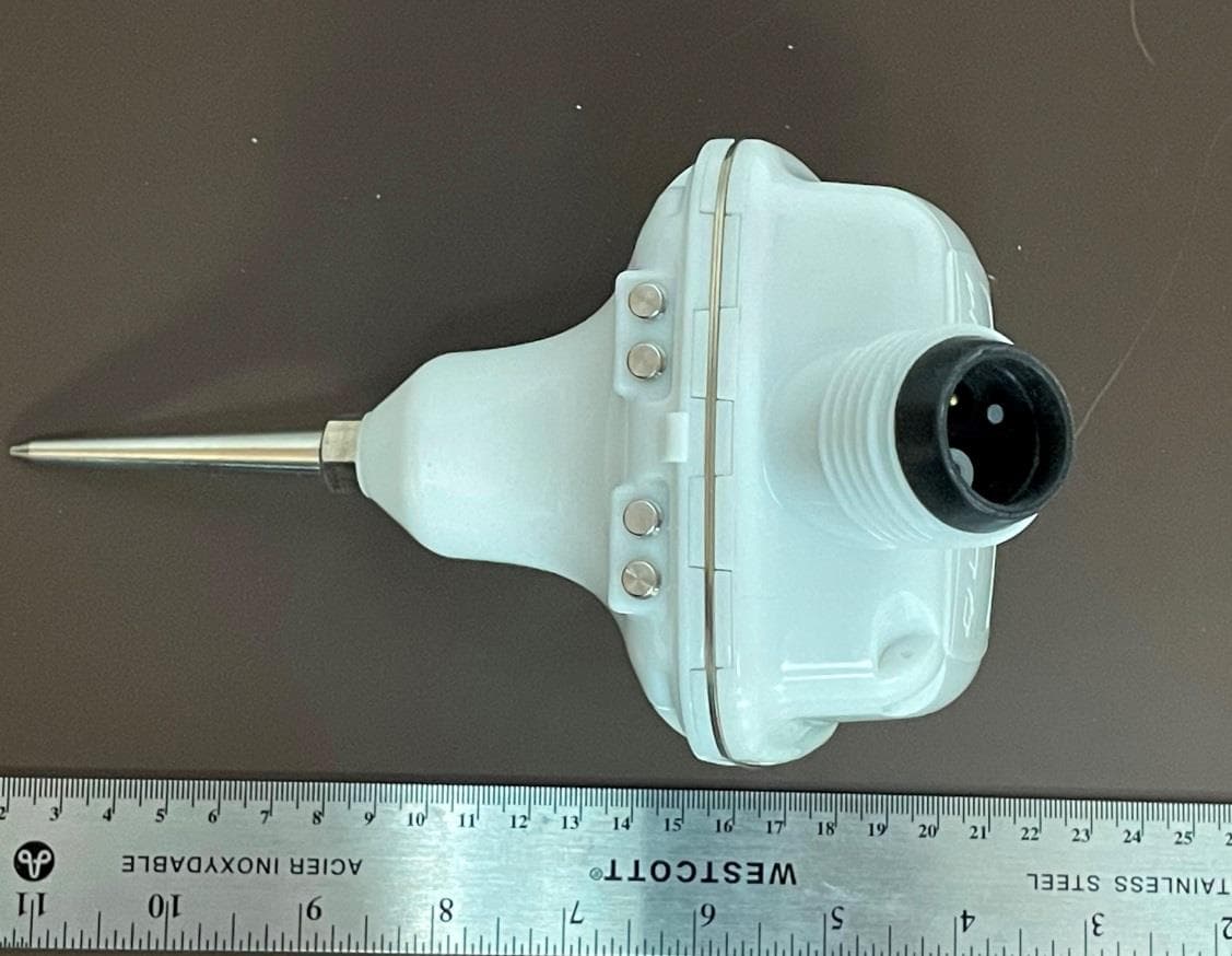
Click to zoom
Application Details
- Equipment Class
- DSS - Part 15 Spread Spectrum Transmitter
- Date of Grant
- Sep 22, 2024
- Application Purpose
- Original Equipment
- Date of Application
- Sep 22, 2024
- Equipment Note
- The Quantum Dual Band HyperQ Node is an all-in-one single component for seismic sensor applications
- Frequency Range
- 902.30000000 - 908.50000000
- Company
- INOVA Systems Corporation
- Country
- Canada
Documents & Files
Document Text
Text extracted from the exhibit documents filed with the FCC. Open a document above to read the original.
Users Manual
Chapter 2 Quantum NODE 15 Chapter 2 Quantum NODE Quantum Node (QN) The Quantum Node is designed to work without the need for radio communication with the Central Recording System. The node acquires GPS signal for timing and communicates locally to the user through Bluetooth Low Energy (BLE) network. The Quantum Node consist of 16GB local data storage, internal battery and integrated vertical 5Hz or 10Hz high-sensitivity phone or a MEMS sensor (Accuseis). The rugged waterproof housing protects the ground station electronics from rough handling of seismic field crews. Features • Compact design and light weight allow easier equipment deployment across challenging terrains and dense vegetation • Rugged watertight casing provides additional protection of ground electronics for extended product life • Bluetooth Low Energy (BLE) technology – delivers communication between the user and equipment to improve field operations involving deployment and equipment status collection with minimal power consumption High-speed USB interface is also included for routine data downloading when connected to the iX Transcriber computer: • Positive Operation LEDs provide instant verification of Node and Sensor Health, Quality of GPS Signal, Battery Voltage • Low power consumption allows up to 50+ days of continuous seismic data recording • Hibernation Mode 16 Hibernation Mode Normally the Node will not be powered on when laying on any side or on upside-down position. Once a node is in upright position, it turns on automatically see: See Node Deployment Typically, the Quantum Node is stored, transported, and carried for deployment in a “Node Carrier” as pictured below. This ensures the Node does not power up (and consume battery) unnecessarily or have false deployments while going to the receiver location. As in the picture below, where a user or shipper handler may mistakenly turn the container on its side. This would result in half the Nodes in “normal operating mode” to be in a “ON” setting and searching for GPS trying to get ready for recording and consuming Battery Hibernation mode is a selection made by the user while the Node is in the Download/Charge rack. On “ hibernate”, see Connectivity A Node set to “Hibernate” will not turn on, no Bluetooth, no GPS and very low battery consumption. Nodes will exit hibernation mode at the time when the unit(s) is docked in a Download and Charge rack. From that point on, unit(s) resume the Quantum's normal operational behaviors Chapter 2 Quantum Node 17 Quantum Node Specifications Quantum Node built in Geophone 18 Quantum Node with external connector This node can be configured (using Quantum Config) to use either the internal built in Geophone or an external geophone such as a Marsh phone. Chapter 2 Quantum Node 19 Quantum Node, internal MEMS Sensor - Accuseis 20 Operation The Quantum Nodes are typically placed at every receiver station. The node turns on automatically after placing it on the ground in upright position. The node LED is flashing orange at the beginning while it runs tests and acquires GPS time fix. Normally after GPS fix is made, the LED starts flashing green (slow) indicating that node is awake and working properly. When LED is flashing red, the node is tilted more than 10° from the vertical position or other error has occurred. The QC Tool can be used to connect to the unit to finish the deployment, perform QC, collect status data or troubleshoot, if required. Quantum Field Deployment, Harvest and QC Tools The QC Tool is used for local communication with the Quantum Nodes (QN). The QC Tool is a rugged Tablet device running the QC Tool software or can be installed on an Android Tablet (OS version 7.0 or greater) supporting BLE (version 4.0 or greater). The QC Tool uses Bluetooth Low Energy (BLE) communication protocol and can quickly acquire QC and status information from the deployed nodes. The QC Tool can also be used to monitor real-time seismic data acquisition by Quantum Nodes in the field. Chapter 2 Quantum Node 21 Node Deployment Before deployment, the nodes should be fully charged and must be pre-configured with survey specific parameters while plugged into docking station and connected to the iX1 Transcriber . The node is off service when laying on any side or on upside-down position. Once node is in upright position, it turns on automatically. Refer to the figure below. INOVA recommends to keep the nodes off service before actual deployment. Depending on the ground condition, there are different scenarios of the node installation. Refer to the figure below. • Optimally, the top of the node should be flushed with the ground. If desired, the node can be buried under a few centimeters of soil. • On the hard surfaces a hole can be drilled to the depth of the spike before installation. • In case of the loose gravel, the shovel can be used to dig a hole which then can be refilled with the same material after node installation. 22 Important Do not use impact tools such as hammers during the node layout. If the nodes have been transported by more than a few hundred kilometers from the last deployment position, it is important to re- acquire the GPS almanac before starting a new project. The nodes must be placed outside with a good sky view. It may take up to 20 minutes to update the GPS satellite almanac and ephemeris data. After setting the node vertically on the ground, it turns on automatically and the LED starts flashing orange while it performs a self-test and acquires a GPS Fix. Once a GPS Fix is acquired, the LED starts flashing green (slow) indicating that node is in the data acquisition mode. Now the node can be accessed by the QC Tool over Bluetooth Low Energy (BLE) network to gather the QC/Status data or troubleshooting, if required. Deep Sleep Mode • Ultra low-power mode • No data acquisition or GPS timing • This mode is automatically initiated when node is tilted more than 30° of upright vertical position Self-Test Mode • Node performs …
Text truncated - open the document above for the full version.
Attestation Statements
U.S. Agent Designation for Service of Process ATTENTION: Federal Communications Commission Authorization and Evaluation Division 7435 Oakland Mills Road Columbia, MD 21046 USA REGARDING: FCC Certification – Section 2.911(d)(7) Information Designated U.S. Agent Company Name: INOVA Geophysical Inc. Contact Name: Paul Akers Street Address: 13000 Executive Dr., Ste.100 City/Province/Zip: Sugar Land, Texas, TX 77478 Telephone No: +1.281.568.2243 Email: [email protected] FRN #: 0035615632 This letter is to confirm that we (“the Designated U.S. Agent) have accepted the responsibility to act as the Designated U.S. Agent for Service of Process as required by section 47 CFR 2.911(d)(7) on behalf of the Applicant noted below. U.S. Agent Signature: Date: Aug 1, 2024 Signed by (Printed Name/Title): PAUL AKERS / Staff Electrical Engineer *This letter is valid indefinitely for all applications submitted within the period of Aug 1, 2024, to July 31, 2029 The Applicant confirms its explicit consent and acknowledges that they must maintain an agent for no less than one year after terminating all marketing and importation OR the conclusion of any Commission-related proceeding involving the equipment. The applicant further acknowledges their responsibility to inform the FCC whenever the Designated U.S. Agent information above changes. Applicant Company name: INOVA Systems Corporation FRN #: 0035615632 Grantee Code: 2BHBH Contact Name: Mark Zhao Street Address: 1769 – 120 Ave NE City/Province/Zip: Calgary, AB, T3K 0S5 Telephone No: (office) 1.403.537.2151 (mobile) 1.403.701.6016 Email: [email protected] Applicant Signature: Date: Aug 1, 2024 (Printed Name/Title): MARK ZHAO/ Hardware Developer
Attestation Statements
Date: Aug 1, 2024 Certification Attestation Statements Attn: Federal Communications Commission Authorization and Evaluation Division 7435 Oakland Mills Road Columbia, MD 21046 USA Subject: Certification Attestation Statements for FCC ID: 2BHBH-95568866 To Whom It May Concern: 47 CFR section 2.911(d)(5)(i) Attestation Statement INOVA System Corporation certifies that as of the date of the application the equipment for which authorization is sought is not “covered” equipment 1 prohibited from receiving an equipment authorization pursuant to section 2.903 of the FCC rules. If the equipment for which the applicant seeks authorization is produced by any of the entities identified on the current Covered List, including affiliates or subsidiaries of the named companies, the applicant must include an explanation on why the equipment is not “covered” equipment. 47 CFR section 2.911(d)(5)(ii) Attestation Statement INOVA System Corporation, (“the applicant”), certifies that, as of the date of the filing of this application, the applicant is not identified on the Covered List (as a specifically named entity or any of its subsidiaries or affiliates) as an entity producing “covered” equipment. Thank you, Mark Zhao Hardware Developer INOVA System Corporation 1 The Commission’s Covered List is published by the Public Safety and Homeland Security Bureau and posted on the Commission’s website. This Covered List, which is periodically updated, identifies particular equipment, produced by particular entities, that constitutes “covered” equipment. https://www.fcc.gov/supplychain/coveredlist .
Cover Letter(s)
Federal Communications Commission Authorization and Evaluation Division 7435 Oakland Mills Road Columbia, MD 21046 USA Date: Aug 1, 2024 SUBJECT: Confidentiality Request regarding application for certification of FCC ID: 2BHBH-95568866 Pursuant to Sections 0.457 and 0.459 of the Commission’s Rules, we hereby request to hold permanently confidential the information accompanying this application as outlined below: Exhibit Type File Name Block Diagram 95568866_BlkDia.pdf Schematics 95568866_Sch.pdf Part List 95568866_PartList.pdf Operational Description 95568866_OpDesc.pdf Tune up 95568866_TuneProc.pdf The above materials contain trade secrets and proprietary information not customarily released to the public. The public disclosure of these materials may be harmful to the applicant and provide unjustified benefits to its competitors. The applicant understands that pursuant to Section 0.457 of the Rules, disclosure of this application and all accompanying documentation not listed above will not be made before the date of the Grant for this application. Regards, Mark Zhao Hardware Developer INOVA Systems Corporation
Cover Letter(s)
Federal Communications Commission Authorization and Evaluation Division 7435 Oakland Mills Road Columbia, MD 21046 USA Date: Aug 1, 2024 SUBJECT: FCC Application for FCC ID: 2BHBH-95568866 To Whom It May Concern: We, the undersigned, hereby authorize Marc Rousseau at Electronics Test Centre – Airdrie (MPB Technologies Inc.) on our behalf, to apply to the Federal Communications Commission on our equipment. Any and all acts carried out by Electronics Test Center – Airdrie (MPB Technologies Inc.) on our behalf shall have the same effect as acts of our own. This is to advise that we are in full compliance with the Anti- Drug Abuse Act. We, the applicant, are not subject to a denial of federal benefits pursuant to Section 5301 of the Anti-Drug Act of 1988, 21 USC853a, and no party to the application is subject to a denial of federal benefits pursuant to that section. Regards, Mark Zhao Hardware Developer INOVA Systems Corporation
External Photos
FCC ID: 2BHBH-95568866 EUT External Photo IC ID: 32788-95568866 Model# FNL41075 and FNL41076 1 st side (Without scale) 2 nd side (Without Scale) FCC ID: 2BHBH-95568866 EUT External Photo IC ID: 32788-95568866 3 rd side (Without Scale) 4 th side (Without Scale) FCC ID: 2BHBH-95568866 EUT External Photo IC ID: 32788-95568866 Top View: Bottom View: FCC ID: 2BHBH-95568866 EUT External Photo IC ID: 32788-95568866 Height (with scale) FCC ID: 2BHBH-95568866 EUT External Photo IC ID: 32788-95568866 1 st side (With scale) 2 nd side (With scale) FCC ID: 2BHBH-95568866 EUT External Photo IC ID: 32788-95568866 3 rd side (With scale) 4 th side (With scale)
ID Label/Location Info
Label for FNL41076: Label for FNL41075, the variant: The label will be laser-etched on top cover of the product:
Internal Photos
FCC ID: 2BHBH-95568866 IC: 32788-95568866 Internal Photos Model# FNL41075 Removing top cover FCC ID: 2BHBH-95568866 IC: 32788-95568866 Internal Photos Top Cover inside View FCC ID: 2BHBH-95568866 IC: 32788-95568866 Internal Photos Enclosure with PCB FCC ID: 2BHBH-95568866 IC: 32788-95568866 Internal Photos Enclosure without PCB FCC ID: 2BHBH-95568866 IC: 32788-95568866 Internal Photos Enclosure after removing PCB mount FCC ID: 2BHBH-95568866 IC: 32788-95568866 Internal Photos Enclosure without Battery FCC ID: 2BHBH-95568866 IC: 32788-95568866 Internal Photos Enclosure without Battery platform FCC ID: 2BHBH-95568866 IC: 32788-95568866 Internal Photos PCB TOP view LoRa Antenna BLE Antenna GEO Phone Connector FCC ID: 2BHBH-95568866 IC: 32788-95568866 Internal Photos PCB Bottom view FCC ID: 2BHBH-95568866 IC: 32788-95568866 Internal Photos Model# FNL41076 Removing top cover FCC ID: 2BHBH-95568866 IC: 32788-95568866 Internal Photos Top Cover inside View FCC ID: 2BHBH-95568866 IC: 32788-95568866 Internal Photos Enclosure with PCB FCC ID: 2BHBH-95568866 IC: 32788-95568866 Internal Photos Enclosure without PCB FCC ID: 2BHBH-95568866 IC: 32788-95568866 Internal Photos Enclosure after removing PCB mounts FCC ID: 2BHBH-95568866 IC: 32788-95568866 Internal Photos Enclosure internal view without Battery platform FCC ID: 2BHBH-95568866 IC: 32788-95568866 Internal Photos Enclosure internal view FCC ID: 2BHBH-95568866 IC: 32788-95568866 Internal Photos PCB TOP view GEO Phone Connector termination LoRa Antenna BLE Antenna FCC ID: 2BHBH-95568866 IC: 32788-95568866 Internal Photos PCB Bottom view
RF Exposure Info
FCC ID: 2BHBH-95568866 Quantum Dual Band HyperQ Node RF Exposure Evaluation 1 The Quantum Dual Band HyperQ Node conduct high-resolution, wide azimuth seismic surveys run on a rechargeable Li-ion battery pack for outdoor use. Quantum Dual Band HyperQ Node is evaluated for RF radiation exposure according to the provisions of FCC §2.1091, MPE guidelines identified in FCC §1.1310 and FCC KDB 447498:2015. Limits for General Population/Uncontrolled Exposure: 47 CFR 1.1310 Table 1 (B) The maximum exposure level to the public from the RF power of the EUT shall not exceed a power density, S as per the respective limits in Table 1 below, at a distance, d, of 20 cm (Mobile condition) from the EUT. TABLE 1—LIMITS FOR MAXIMUM PERMISSIBLE EXPOSURE (MPE) Frequency range (MHz) Electric field strength (V/m) Magnetic field strength (A/m) Power density (mW/cm2) Averaging time (minutes) Limits for General Population/Uncontrolled Exposure 0.3-1.34 614 1.63 *100 30 1.34-30 824/f 2.19/f *180/f2 30 30-300 27.5 0.073 0.2 30 300-1,500 f/1500 30 1,500-100,000 1.0 30 Where f is in MHz *Plane-wave equivalent power density Therefore: MPE for Quantum HyperQ node from 902.3 MHz to 908.5 MHz. The worst-case scenario for LoRa Radio is at 902.3 MHz is S = 0.6015 mW/cm 2 , for General Population/Uncontrolled Exposure And for BLE radio is S = 1 mW/cm 2 , for General Population/Uncontrolled Exposure LoRa RF conducted power measurement and antenna gain as per ETC test reports i27e24a224_DTS & DSS are reported below. The worst-case value is in highlighted below TX Frequency (MHz) Max Conducted RF Output after Duty Cycle correct factors (dBm) Max. antenna gain (dBi) EIRP (dBm) EIRP (mW) LoRa 125 KHz FHSS 902.3 17.4 -3.0 14.4 27.54 905.3 17.3 -3.0 14.3 26.92 908.5 17.1 -3.0 14.2 26.30 2402 0.15 -0.0 0.15 1.04 BLE 2440 -0.27 -0.0 -0.27 0.94 2480 -0.38 -0.0 -0.38 0.92 Maximum output power limitation for BLE 6 -0.0 6 3.98 Maximum output power limitation for LoRa 22 -3.0 19 79.43 Note: The BLE and LoRa radios can operate simultaneously. FCC ID: 2BHBH-95568866 Quantum Dual Band HyperQ Node RF Exposure Evaluation 2 Conclusion Using worst case scenario with maximum output power, the highest measured EIRP or [P*G(numeric gain)] value for both radio using max output power limitation BLE transmitter: 3.98 mW LoRa transmitter: 79.43 mW Total Transmit Power (simultaneous transmit condition): BLE Transmitter power + LoRa transmitter power : 3.98 mW + 79.43 mW : 83.41 mW Total Transmit Power (simultaneous transmit condition) rounded up: 84 mW Using the highest total transmitted power at a distance of 20 cm in the equation below: S = EIRP / ( 4πR 2 ) Where: S, power density in ‘mW/cm 2 ’ EIRP, Effective Isotropic Radiated Power in ‘mW’ R, distance to the center of the radiation of the antenna in ‘cm’ The RF exposure from the radio is less than the limit specified as shown below and meets the exemption criteria. S (mW/cm 2 ) = (84 mW) / (4 x π x 20²) S = 0.016711269 mW/cm 2 <<< 0.6015 mW/cm 2 (max limit) Rounded up S = 0.017 mW/cm 2 <<<<<<<<<<<<<<< 0.6015 mW/cm 2 (max limit) To determine the minimum safe distance R = √ [EIRP / (4πS)] R = √ [84 / (4π x 0.6015)] R = 3.333626158 cm Rounded up R = 3.4 cm The manufacturer manual specified a minimum safe distance of 20 cm.
Test Report
This report shall not be reproduced, except in full, without prior written approval of MPB Technologies Page 1 of 52 Test Report Prepared By: Electronics Test Centre 27 East Lake Hill Airdrie, Alberta Canada T4A 2K3 [email protected] http://www.etc-mpb.com Telephone: 1-403-912-0037 ETC Report #: i27e24a224_DSS Release 1 Report date: September 19, 2024 EMC testing of the INOVA Systems Corporation Quantum Dual Band HyperQ Node in accordance with FCC Part 15.247and ANSI C63.10: 2013 as referenced by FCC OET KDB 558074 D01 15.247 Meas Guidance v05r02. FCC ID: 2BHBH-95568866 Test Dates: 2024-06-18 to 2024-06-21 Test Personnel: Janet Mijares/Brendan Van Hee Prepared for: INOVA Systems Corporation 1769-120 Avenue NE Calgary, Alberta Canada T3K 0S5 Telephone: 1-403-537-2134 _________________________ _________________________ Imran Akram Marc Rousseau [email protected] [email protected] EMC Technologist QA Manager Electronics Test Centre (Airdrie) Electronics Test Centre (Airdrie) Test Sample: Quantum Dual Band HyperQ Node FCC ID: 2BHBH-95568866 FCC Part 15.247 Report #: i27e24a224_DSS Release 1 This report shall not be reproduced, except in full, without prior written approval of MPB Technologies Page 2 of 52 REVISION RECORD ISSUE DATE AUTHOR REVISIONS DRAFT 1 2024-06-20 I. Akram Initial draft submitted for review. DRAFT 1 2024-09-06 I. Akram Updated the FCC ID number Release 1 2024-09-19 I. Akram Sign Off Test Sample: Quantum Dual Band HyperQ Node FCC ID: 2BHBH-95568866 FCC Part 15.247 Report #: i27e24a224_DSS Release 1 This report shall not be reproduced, except in full, without prior written approval of MPB Technologies Page 3 of 52 TABLE OF CONTENTS 1.0 INTRODUCTION 5 1.1 Scope .........................................................................................................................5 1.2 Applicant ....................................................................................................................5 1.3 Test Sample Description ............................................................................................5 1.4 General Test Conditions ............................................................................................5 1.5 Reference Standards .................................................................................................6 1.6 Test Methodology .......................................................................................................6 1.6.1 Variations in Test Methodology ..................................................................... 6 1.6.2 Test Sample Verification, Configuration & Modifications .............................. 6 1.6.3 Uncertainty of Measurement: ............................................................................ 6 2.0 TEST CONCLUSION 7 2.1 Duty Cycle: .................................................................................................................8 2.1.1 Test Guidance: ANSI C63.10-2013, Clause 11.6 / FCC OET KDB 558074 clause 6 ...................................................................................................................... 8 2.1.2 Test Equipment ............................................................................................. 8 2.1.3 Duty Cycle ..................................................................................................... 8 2.2 AC Main Power Line Conducted Emissions: N/A ....................................................10 2.3 Occupied Bandwidth ................................................................................................11 2.3.1 Test Guidance: ANSI C63.10-2013, Clause 6.9.2 & 6.9.3/ FCC OET KDB 558074 11 2.3.2 Deviations From The Standard: .................................................................. 11 2.3.3 Test Equipment ........................................................................................... 11 2.3.4 Test Sample Verification, Configuration & Modifications ............................ 12 2.3.5 Channel Occupied Bandwidth Data: ........................................................... 12 2.4 Max Average Output Power .....................................................................................14 2.4.1 Test Guidance: ANSI C63.10-2013, Clause 11.9.2.2.4 / FCC OET KDB 558074 14 2.4.2 Deviations From The Standard: .................................................................. 15 2.4.3 Test Equipment ........................................................................................... 15 2.4.4 Test Sample Verification, Configuration & Modifications ............................ 15 2.4.5 Max Output Power Data: DSS .................................................................... 15 2.5 Power Spectral Density ............................................................................................18 2.5.1 Test Guidance: ANSI C63.10-2013, Clause 11.10.5 / FCC OET KDB 558074 18 2.5.2 Deviations From The Standard: .................................................................. 18 2.5.3 Test Equipment ........................................................................................... 18 2.5.4 Test Sample Verification, Configuration & Modifications ............................ 19 2.5.5 Average PSD Data ...................................................................................... 19 2.6 Band Edge Attenuation ............................................................................................21 2.6.1 Test Guidance: ANSI C63.10-2013 Clause 6.10.4 & 7.8.6, 6.10.6 / FCC OET KDB 558074 ............................................................................................................. 21 2.6.2 Deviations From The Standard: .................................................................. 22 2.6.3 Test Equipment ........................................................................................... 22 2.6.4 Test Sample Verification, Configuration & Modifications ............................ 22 2.6.5 Band Ed…
Text truncated - open the document above for the full version.
Test Report
ISM/LoRa Antenna NAN - F SERIES www.NICcomp.com | Tech Support: [email protected] Page | 1 FEATURES • Stable and reliable in performances • Compact size • RoHS compliant APPLICATIONS • ISM 868/915 Bands • Smart meters • Wireless alarm and security system • Industrial monitoring and control • IOT applications SPECIFICATIONS Electrical Frequency Range 863 ~ 873 MHz 910 ~ 920 MHz Center Frequency 868 MHz 915 MHz Polarization Linear Impedance 50Ω Dimensions (mm): Body Length (A) 35 ± 2.0 Width (C) 7.0 ± 1.0 Cable Length (B) 38 ± 5.0 Cable Type RF1.13 Connector Type IPEX (MHF I) NAN-F 868-915 DB - 105 X 38 A F F = RoHS compliant A = RF1.13 Cable 38 = Cable length in mm X = IPEX Connector 105 = Version Code (See page 7) DB = Dual Band 868 – 915 = Center Frequency NAN-F = Series Item Name Material Color 1 NAN-F_FPC PI Black 2 I-PEX & RF1.13 FEP Gray RoHS Compliant includes all homogeneous materials (see part numbering system for details) ISM/LoRa Antenna NAN - F SERIES www.NICcomp.com | Tech Support: [email protected] Page | 2 Setup: S-Parameters (Impedance, Return Loss, and VSWR) • Equipment - Network Analyzer (Agilent E5071A) Radiation Patterns ( Gain, Efficiency, 2D gain patterns and 3D gain Patterns) • Equipment- Anechoic Chamber, Network Analyzer (Agilent E5071C), Standard Horn. ISM/LoRa Antenna NAN - F SERIES www.NICcomp.com | Tech Support: [email protected] Page | 3 Antenna Placement Return Loss ISM/LoRa Antenna NAN - F SERIES www.NICcomp.com | Tech Support: [email protected] Page | 4 Radiation Efficiency 863 ~ 873 MHz ISM/LoRa Antenna NAN - F SERIES www.NICcomp.com | Tech Support: [email protected] Page | 5 Radiation Efficiency 910 ~ 920 MHz ISM/LoRa Antenna NAN - F SERIES www.NICcomp.com | Tech Support: [email protected] Page | 6 RADIATION PATTERNS 3D Gain Pattern ( Radiation Pattern @ 868 MHz) (unit: dBi) 3D Gain Pattern ( Radiation Pattern @ 915 MHz) (unit: dBi) ISM/LoRa Antenna NAN - F SERIES www.NICcomp.com | Tech Support: [email protected] Page | 7 Version History and Status Version Date Issued Details Status 105 October 18 th 2022 Initial Release Inova DOT Program Supported Please reach out to NIC for any customization requests and other inquiries: NIC Technical Support: [email protected] Compliance Support: [email protected] Introduction This document describes the design, fabrication, and radio electrical characterization (S11 parameter and radiation) of a set of seven antennas associated with their electronic board, operating on the ISM 2.45 GHz frequency band and available for the STM32WB Series microcontrollers. The seven antenna types are: • Monopole T-shaped antenna • Monopole L-shaped antenna • Inverted F Antenna – IFA • Microstrip meandered monopole antenna • IFA metal plane antenna • Yagi-Uda antenna • Chip antenna On-board antennas reference design for the STM32WB Series MCUs AN5434 Application note AN5434 - Rev 1 - January 2020 For further information contact your local STMicroelectronics sales office. www.st.com Figure 17. Simulated radiation pattern for the simplified and complete models at 2.45 GHz: (a) φ=0° (XZ plane), (b) φ=90° (YZ plane), (c) Θ=90° (XY plane) 3.5Inverted F antenna - IFA 3.5.1Configuration Numerous research studies are conducted to analyze the Inverted-F antenna such as in [4] where the authors present experimental observations about the IFA performances at the frequency 1.8 GHz for portable handsets. The 3D inverted-F antenna is also explored in the presence of parasitic elements in 1989 by H.Nakano and his colleagues[5], to reveal the behavior of the input impedance and to widen the impedance bandwidth. Similarly, the geometry and dimensions of the proposed inverted F antenna conceived here, are shown in Figure 18. The simplified and complete designs are also investigated here to ensure good accuracy results. This design is compact compared to the previous ones with an overall size of 52 x 30 mm 2 . Additionally, to optimize the location of the radiating element on the small PCB, an L-shaped extension is added to achieve resonance at the desired frequency without increasing the PCB dimensions as presented in Figure 18 (a). Figure 18. Inverted-F antenna configuration: (a) simplified model (b) complete model 3.5.2Simulation results The proposed IFA models are designed also on the FR4 substrate based on dimensions shown in Figure 18. The simulated return loss for the simplified model is shown as a black line, while the complete one is as a dashed red line in Figure 19. A slight shift of the resonance frequency can be observed when the antenna is placed on its real environment. However, a good reflection coefficient is maintained over the ISM range of frequencies. Notice that the resonance associated with the chip PCB is not excited with this compact antenna topology and the matching frequency band is consequently narrower. AN5434 Inverted F antenna - IFA AN5434 - Rev 1 page 13/44 In Figure 20, the simulated input impedance variation within frequency is exposed. An insignificant difference is observed in terms of real and imaginary parts when switching to a complete model. Figure 19. Simulated return loss versus frequency for simple and complete models Figure 20. Simulated input impedance versus frequency for simple and complete models AN5434 Inverted F antenna - IFA AN5434 - Rev 1 page 14/44 Figure 21 illustrates the total efficiency of the IFA antenna against frequency. A decrease of 1.6 % is observed in the case of the complete model compared to the simple one. Figure 22 shows the 2D radiation pattern in terms of gain, in three different planes at 2.45 GHz. Omnidirectional radiation is observed in the plane Θ=90°. Notice that a good agreement is achieved between the complete and simplified models, except the cross-polarization level that increases in the φ=0° and Θ=90°. The asymmetry of the diagram is observable in the φ=0° cut plane due to antenna topology. Figure 21. Simulated efficiency versus frequency for simple and complete models Figure 22. Si…
Text truncated - open the document above for the full version.
Test Setup Photos
FCC ID: 2BHBH-95568866 IC: 32788-95568866 EUT Test Setup Photo EUT Antenna Port Conducted Measurement Test Setup: FCC ID: 2BHBH-95568866 IC: 32788-95568866 EUT Test Setup Photo Radiated Emission below 30 MHz Test Setup: FCC ID: 2BHBH-95568866 IC: 32788-95568866 EUT Test Setup Photo Radiated Emission 30 MHz to 1 GHz Test Setup: TX & RX Mode FCC ID: 2BHBH-95568866 IC: 32788-95568866 EUT Test Setup Photo Radiated Emission 1 GHz – 18 GHz Test Setup: TX Mode FCC ID: 2BHBH-95568866 IC: 32788-95568866 EUT Test Setup Photo Radiated Emission 18 GHz – 26 GHz Test Setup: TX Mode FCC ID: 2BHBH-95568866 IC: 32788-95568866 EUT Test Setup Photo Radiated Emission 1 GHz – 12.5 GHz Test Setup: RX Mode
Contact Information
Applicant
Mark Zhao(Hardware Developer)
Test Firm
Electronics Test Centre-Airdrie (MPB Technologies)Marc Rousseau
Technical Specifications
| # | Rule Parts | Frequency Range | Power Output | Emission |
|---|---|---|---|---|
| 1 | 15C | 902.3 MHz - 908.5 MHz | 55.00 mW | F1D |