2BK6C-T10Yebos stylus pen
Shenzhen Jinji Digital Technology Co., Ltd.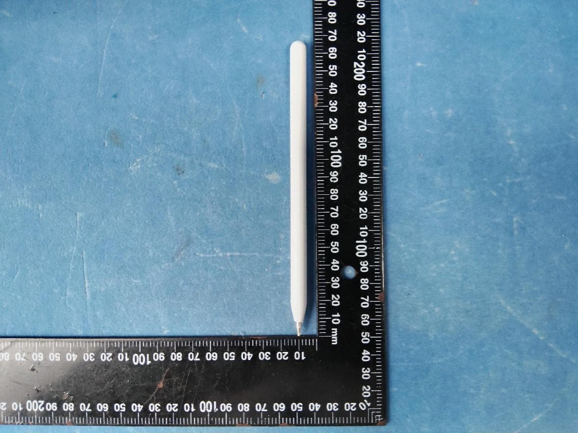
Click to zoom
Application Details
- Equipment Class
- DTS - Digital Transmission System
- Date of Grant
- Oct 08, 2024
- Application Purpose
- Original Equipment
- Date of Application
- Oct 08, 2024
- Equipment Note
- Yebos stylus pen
- Frequency Range
- 2402.00000000 - 2480.00000000
- Country
- China
Documents & Files
Document Text
Text extracted from the exhibit documents filed with the FCC. Open a document above to read the original.
Users Manual
Product diagram: Key On/Off Shortcut key Charging port Turn on the Bluetooth search and find : Yebos T10 Bluetooth name, click Connect (wait for 10s Bluetooth name to appear when you connect for the first time) (If the connection is displayed, the connection is successful)(The percentage of successfully connected battery is displayed) Product name: IPus Capacitor Pen Product model :T10 Main functions: drawing, writing, notes, custom shortcut keys, gain adjustment Product material: Metal (shell spraying process) Product size: Pen tip 1.45* Diameter 9* length 165mm Net weight: about 16g Product accessories :Pencilx1 Data cable x1 manual x1 nib Pilot lamp Button function/Light indicator: Bluetooth connection: YEBOS T10 Pencil Instructions for use: *Key On/Off Press for 0.5 seconds Power on Hold down for 3 seconds Power O *Return to main screen (default) *Pilot lamp Product parameter: Connect NoteYebos App:自定义快捷键功能: Exclusive note APP QR code:Signal conditioning function use tutorial: Start your productive recording journey Scan the QR code to download the NoteYebos APP 1. On/off 2.HOME button 3. Power button 4. Brightness plus 5. Brightness reduction 6. Task Bar 7. Volume plus 8. Volume reduction 9. Previous page 10. Next page 11. Mute 12. Search 13. Take pictures 14. Take quick screenshots 15. Edit the screenshot 16. Revocation 17. Pen/eraser switch 18. Play/pause 19. Previous song 20. Next song 21. Create quickly 22. A ruler Take photos (default) Click Return to main interface (default) Double-click (Please charge the device in time) When the capacitor pen is working: 70%-100% Blue light 10%-70% Green light Below 10% The red light flashes 100% Always on blue light 80%-99% Green light 0%-80% Red light When the capacitor pen is charging: Scan the QR code above or download NoteYebos in the App store After the connection in the setup is successful, Note YebosApp will automatically connect the capacitor pen Open the home page of NoteYebos App and click the Bluetooth icon in the upper right corner to view the capacitor pen connection status Click the Bluetooth icon on the home page of the App to set the shortcut key customization function Gain control function:Change the smart shutdown time: 1. Open the home page of NoteYebos App and click Bluetooth in the upper right corner The icon can adjust the gain of the capacitor pen 2. Click the writing posture button to select the writing posture 3. Click the smart shutdown button, select the time, and click Finish The smart shutdown time of the capacitor pen can be modified; (The smart shutdown function requires the capacitor pen to be at rest without operation) 4. Click the signal adjustment button to adjust the signal of the capacitor pen (If there is a broken contact problem, please increase the signal first for adjustment) 5. Change the nib: Before switching the nib, ensure that you have switched the nib Open the home page of NoteYebos App and click right Bluetooth icon in the upper corner, click Smart shut down pressButton, select the time, click finish to power Pen smart shutdown time modification; Smart shutdown function requires capacitor pen at rest without In the operating state) Nib change: Turn the pen tip clockwise and pull it offThen take the new tip and screw it in counterclockwise Touch Prevention mode is available for iPad use from 2018 and 2019 onwards * The iPad must be upgraded to iOS13.4 and above. Please read all instructions and warnings before using this product, Non-standard use will cause damage to the product or personal safety. Instructions for use: Compatible device: * If your iPad has been previously paired with Apple Pencil, unpair it before using this device Matters needing attention: 1. this product is not a children's toy, please ensure that infants and toddlers do not play with this product as a toy: children under 12 years old, please use under the care of a guardian; 2. the conversion rate of the capacitor pen, so the capacitor pen battery capacity is not equal to the amount of rechargeable; 3. please charge your capacitor pen regularly (recommended once every 3 months) to maintain long-term service life; 4. the product is prohibited from hard beating, heavy pressure: do not collide with sharp or sharp objects when using or storing; 5. this product is not waterproof, do not use when the product is wet and dry in time: do not use again after completely soaking water and internal water, to avoid accidents and dangers; 6. the product built-in battery, it is prohibited to use and store in high temperature (higher than 60 ° C) environmental space, such as stove, heater near, exposed car room, etc. : to avoid battery explosion and other accidents; 7. do not squeeze, disassemble the battery or put the battery in a high temperature environment for a long time (above 60 ° C), otherwise there may be leakage or explosion risk; 8. if the consumer uses the capacitor pen adapter to charge, the power adapter input rated voltage should be within 5V, rated current 2A, and obtain the national mandatory safety certification to use; 9. This product uses lithium battery. Overcharge or pass will affect the service life of the product, please charge in time or disconnect the power after full; 10. product failure, please contact the sales or the company in time, it is prohibited to disassemble and repair attempts to decompose or change the structure of the product, so as not to cause unnecessary failure and danger. T10 Pencil 产品示意图: 按键开/关 快捷功能键 充电口 开机后指示灯常亮进入设置打开蓝牙搜索到: Yebos T10 蓝牙名,点击连接(第一次连接时 需等待10s蓝牙名出现) (显示已连接即为连接成功)(连接成功电量百分比显示) 产品名称:益博思电容笔 产品型号:T10 主要功能:绘画、书写、笔记、自定义快捷键、增益调节 产品材质:金属(外壳喷涂工艺) 产品尺寸:笔尖1.45*直径9*长165mm 产品净重:约16g 产品配件:Pencilx1 数据线x1 说明书x1 笔尖 指示灯 按键功能/灯光指示: 蓝牙连接: YEBOS T10 Pencil 使用说明: (可开机直接使用,或连接 蓝牙解锁更多功能) (It can be used directly when powered on, or connected to Bluetooth to unlock more functions) *按键开/关 短按0.5秒 开机 长按3秒 关机 *自定义快捷功能键 *指示灯 产品参数: 连接NoteYebos App:自定义快捷键功能: 专属笔记APP:信号调节功能使用教程: 开启高效记录之旅 扫码观看视频 Scan the QR code t…
Text truncated - open the document above for the full version.
Attestation Statements
2.911(d)(5)(i)EquipmentTypeAttestationv1.2 ShenzhenJinjiDigitalTechnologyCo.,Ltd. Section2.911(d)(5)(i)Certification–EquipmentType Companyname:ShenzhenJinjiDigitalTechnologyCo.,Ltd. Address:Room902-03,BuildingG-2,GalaxyWORLD,NankengCommunity,BantianStreet, Shenzhen,China ProductName:Yebosstyluspen FCCID:2BK6C-T10 Model(s):T10 2.911(d)(5)(i)EquipmentType We,[ShenzhenJinjiDigitalTechnologyCo.,Ltd.]certifythattheequipmentforwhich authorizationissoughtthroughcertificationisnot: Prohibitedfromreceivinganequipmentauthorizationpursuantto§2.903;oftheFCCrules. Identifiedasanequipmenttypeinthe“CoveredList” NOTE1 Yourssincerely, Name:YongMaDate:09-29-2024 TitleandCompanyname:generalmanager/ShenzhenJinjiDigitalTechnologyCo.,Ltd. NOTE1 “CoveredList”;istheListofEquipmentandServicesCoveredBySection2ofTheSecureNetworksAct,availableat https://www.fcc.gov/supplychain/coveredlist References; 1)986446D01CoveredEquipmentv01 https://apps.fcc.gov/oetcf/kdb/forms/FTSSearchResultPage.cfm?switch=P&id=325672 2)FederalRegisterdocument2022-28263publishedon02/06/23 https://www.federalregister.gov/documents/2023/02/06/2022-28263/protecting-against-national-security-threats-to-the-com munications-supply-chain-through-the
Attestation Statements
2.911(d)(5)(ii)ApplicantAttestationv1.3 ShenzhenJinjiDigitalTechnologyCo.,Ltd. Section2.911(d)(5)(ii)Certification–Applicant(CoveredList) Companyname:ShenzhenJinjiDigitalTechnologyCo.,Ltd. Address:Room902-03,BuildingG-2,GalaxyWORLD,NankengCommunity,BantianStreet, Shenzhen,China ProductName:Yebosstyluspen FCCID:2BK6C-T10 Model(s):T10 2.911(d)(5)(ii)Applicantfiling We,[ShenzhenJinjiDigitalTechnologyCo.,Ltd.]certifythat,asofthedateofthefilingofthe application,theapplicantisnotidentified NOTE1 onthe“CoveredList” NOTE2 ,establishedpursuant to§1.50002ofthischapter,asanentityproducingcoveredcommunicationsequipment. Yourssincerely, Name:YongMaDate:09-29-2024 TitleandCompanyname:generalmanager/ShenzhenJinjiDigitalTechnologyCo.,Ltd. NOTE1 Deleteoptionnotapplicabletothisapplication. NOTE2 “CoveredList”;istheListofEquipmentandServicesCoveredBySection2ofTheSecureNetworksAct,availableat https://www.fcc.gov/supplychain/coveredlist References; 1)986446D01CoveredEquipmentv01 https://apps.fcc.gov/oetcf/kdb/forms/FTSSearchResultPage.cfm?switch=P&id=325672 2)FederalRegisterdocument2022-28263publishedon02/06/23 https://www.federalregister.gov/documents/2023/02/06/2022-28263/protecting-against-national-security-threats-to-the-com munications-supply-chain-through-the 2.911(d)(5)(ii)ApplicantAttestationv1.3
Attestation Statements
ShenzhenJinjiDigitalTechnologyCo.,Ltd. U.S.AgentLetterofAttestation To:FederalCommunicationsCommission 7435OaklandMillsRoad,Columbia,MD21046,USA Date:09-29-2024 Ref: AttestationStatement–Part 2.911(d)(7)filing FCCID:2BK6C-T10 ShenzhenJinjiDigitalTechnologyCo.,Ltd.certifiesthat,asofthedateofthefilingofthe Address: 1200BroadwaySt.APT329,LosAngeles,CA90015 Signature application,THREESTONESMEDIALLCisourdesignatedU.S.agentforserviceofprocessfor theabovereferenceFCCID.Theapplicantacceptstomaintainanagentforserviceofprocessin theUnitedStatesfornolessthanoneyearaftereitherthegranteehaspermanentlyterminatedall marketingandimportationoftheapplicableequipmentwithintheU.S.,ortheconclusionofany Commission-relatedadministrativeorjudicialproceedinginvolvingtheequipment,whicheverislater. TheapplicantfurtheracknowledgesitisourresponsibilitytoinformtheFCCwhenevertheagent informationchanges. THREESTONESMEDIALLCunderstanditistheagent'sobligationtoacceptserviceofprocessin theUnitedStatesformattersrelatedtotheapplicableequipment,andatthephysicalU.S.address andemailaddress. DesignatedU.S.Agent CompanyName: THREESTONESMEDIALLC FRN:0033401761 GC:2A99E : ContactPerson:SijieZhang Tel:+12679093692 Applican Email: [email protected] t CompanyName:ShenzhenJinjiDigitalTechnologyCo.,Ltd. Address: Room902-03,BuildingG-2,GalaxyWORLD,Nankeng Community,BantianStreet,Shenzhen,China Signature: ContactPerson:YongMa FRN:0035964436 GC:2BK6C Email:[email protected]
Cover Letter(s)
ShenzhenJinjiDigitalTechnologyCo.,Ltd. OfficeofEngineeringTechnology FederalCommunicationsCommission 7435OaklandMillsRoad Columbia,MD21046 USA Date:09-29-2024 Subject;RequestforConfidentiality FCCID:2BK6C-T10 ToWhomItMayConcern, PursuanttotheprovisionsoftheCommission’srulesTitle47Sections§0.457and§0.459,we arerequestingtheCommissiontowithholdthefollowingattachment(s)asconfidential documentsfrompublicdisclosureindefinitely. Thesedocumentscontaindetailedsystemandequipmentdescriptionsandareconsideredas proprietaryinformationinoperationoftheequipment.Thepublicdisclosureofthesedocuments mightbeharmfultoourcompanyandwouldgivecompetitorsanunfairadvantageinthemarket. SchematicDiagram BlockDiagram PartsList OperationalDescription Tune-upProcedure Inadditionaltoabovementioneddocuments,inordertocomplywiththemarketingregulations inTitle47CFR§2.803andtheimportationrulesinTitle47CFR§2.1204,whileensuringthat businesssensitiveinformationremainsconfidentialuntiltheactualmarketingofnewly authorizeddevices,werequestShortTermConfidentialityofthefollowingattachment(s); ExternalPhotos TestSetupPhotos InternalPhotos UserManual For45days,pursuanttoPublicNoticeDA04-1705. OR For180dayspursuanttoKDB726920D01. Itisourunderstandingthatallmeasurementtestreports,FCCIDlabelformatand correspondenceduringthecertificationreviewprocesscannotbegrantedasconfidential documentsandthisinformationwillbeavailableforpublicreviewoncethegrantofequipment authorizationisissued. Sincerely, Signature: Name:YongMa Title:generalmanager
Cover Letter(s)
ShenzhenJinjiDigitalTechnologyCo.,Ltd. LetterofAuthorization Company:ShenzhenJinjiDigitalTechnologyCo.,Ltd. Address:Room902-03,BuildingG-2,GalaxyWORLD,NankengCommunity,Bantian Street,Shenzhen,China ProductName:Yebosstyluspen ModelNumber(s):T10 ProductDescription:Yebosstyluspen WeauthorizeMiCOMLabsInc.,575BoulderCourt,Pleasanton,California94566,USA, toactonourbehalfonallmattersconcerningthecertificationofabovenamed equipment. WedeclarethatMiCOMLabsInc.isallowedtoforwardallinformationrelatedtothe approvalandcertificationofequipmenttotheregulatoryagenciesasrequiredandto discussanyissuesconcerningtheapprovalapplication.Anyandallactscarriedoutby MiCOMLabsonourbehalfshallhavethesameeffectasactsofourown. Signature:Date:09-29-2024 Name:YongMa Title:generalmanager Company:ShenzhenJinjiDigitalTechnologyCo.,Ltd.
External Photos
FCCID:2BK6C-T10 FCCID:2BK6C-T10 FCCID:2BK6C-T10 FCCID:2BK6C-T10
ID Label/Location Info
FCCID:2BK6C-T10 Label Size:10mm*8mm FCCID:2BK6C-T10 LabelLocation
Internal Photos
FCCID:2BK6C-T10 FCCID:2BK6C-T10 FCCID:2BK6C-T10 ANT FCCID:2BK6C-T10
RF Exposure Info
RFExposureevaluation FCCID2BK6C-T10 ProductNameYebosstyluspen ModelNo.T10 ListedModel(s)-- ExposurecategoryGeneralpopulation/uncontrolledenvironment EUTTypeProductionUnit DeviceTypePortableDevice 1.Reference ANSIC95.1–1999:IEEEStandardforSafetyLevelswithRespecttoHumanExposureto RadioFrequencyElectromagneticFields,3kHzto300GHz. FCCKDBpublication447498D01GeneralRFExposureGuidancev06:MobileandPortable DevicesRFExposureProceduresandEquipmentAuthorizationPolicies. FCCCFR47part11.1310:Radiofrequencyradiationexposurelimits. FCCCFR47part22.1093:Radiofrequencyradiationexposureevaluation:portabledevices 2.Requirement AccordingtoKDB447498D01GeneralRFExposureGuidancev06Section4.3.1Standalone SARtestexclusionconsiderations:“UnlessspecificallyrequiredbythepublishedRFexposure KDBprocedures,standalone1-gheadorbodyand10-gextremitySARevaluationforgeneral populationexposureconditions,bymeasurementornumericalsimulation,isnotrequired whenthecorrespondingSARTestExclusionThresholdcondition,listedbelow,issatisfied. Thesetestexclusionconditionsarebasedonsource-basedtime-averagedmaximum conductedoutputpoweroftheRFchannelrequiringevaluation,adjustedfortune-uptolerance, andtheminimumtestseparationdistancerequiredfortheexposureconditions.22The minimumtestseparationdistanceisdeterminedbythesmallestdistancefromtheantenna andradiatingstructuresoroutersurfaceofthedevice,accordingtothehostformfactor, exposureconditionsandplatformrequirements,toanypartofthebodyorextremityofauser orbystander(see5)ofsection4.1).ToqualifyforSARtestexclusion,thetestseparation distancesappliedmustbefullyexplainedandjustifiedbytheoperatingconfigurationsand exposureconditionsofthetransmitterandapplicablehostplatformrequirements,typicallyin theSARmeasurementorSARanalysisreport,accordingtotherequiredpublishedRF exposureKDBprocedures.WhennootherRFexposuretestingorreportingisrequired,a statementofjustificationandcompliancemustbeincludedintheequipmentapproval,inlieuof theSARreport,toqualifyfortheSARtestexclusion.Whenrequired,thedevicespecific conditionsdescribedintheotherpublishedRFexposureKDBproceduresmustbesatisfied beforeapplyingtheseSARtestexclusionprovisions;forexample,handheldPTTtwo-way radios,handsets,laptops&tabletsetc.23” [(max.powerofchannel,includingtune-uptolerance,mW)/(min.testseparationdistance, mm)]·[√f(GHz)]≤3.0for1-gSARand≤7.5for10-gextremitySAR,where: •f(GHz)istheRFchanneltransmitfrequencyinGHz •PoweranddistanceareroundedtothenearestmWandmmbeforecalculation •Theresultisroundedtoonedecimalplaceforcomparison •3.0and7.5arereferredtoasthenumericthresholdsinthestep2below Thetestexclusionsareapplicableonlywhentheminimumtestseparationdistanceis≤50mm andfortransmissionfrequenciesbetween100MHzand6GHz.Whentheminimumtest separationdistanceis<5mm,adistanceof5mmaccordingto5)insection4.1isappliedto determineSARtestexclusion. Whenoneofthefollowingtestexclusionconditionsissatisfiedforallcombinationsof simultaneoustransmissionconfigurations,furtherequipmentapprovalisnotrequiredto incorporatetransmittermodulesinhostdevicesthatoperateinthemixedmobileandportable hostplatformexposureconditions.Thegranteeisresponsiblefordocumentingthisaccording toClassIpermissivechangerequirements.AntennasthatqualifyforstandaloneSARtest exclusionmustapplytheestimatedstandaloneSARtodeterminesimultaneoustransmission testexclusion. a)The[∑of(thehighestmeasuredorestimatedSARforeachstandaloneantenna configuration,adjustedformaximumtune-uptolerance)/1.6W/kg]+[∑ofMPEratios]is≤ 1.0. b)TheSARtopeaklocationseparationratiosofallsimultaneouslytransmittingantennapairs operatinginportabledeviceexposureconditionsareall≤0.04,andthe[∑ofMPEratios]is≤ 1.0. 3.ConductedPeakOutputPower ModulationPacketTypeChannel PeakOutput Power (dBm) PeakOutput Power (mW) GFSKBLE1M 03.282.13 192.911.95 392.321.7 GFSKBLE2M 03.342.16 193.232.1 392.681.85 4.ManufacturingTolerance BLE1M ChannelChannel0Channel19Channel39 Target(dBm)3.02.02.0 Tolerance±(dB)1.01.01.0 BLE2M ChannelChannel0Channel19Channel39 Target(dBm)3.03.02.0 Tolerance±(dB)1.01.01.0 5.EvaluationResult Band/Modef(GHz) Antenna Distance (mm) RFoutputpower SARTest Exclusion Threshold SARTest Exclusion dBmmW BLE2.44054 2.51 0.7849<3.0Yes Remark: 1.Outputpowerincludingtuneuptolerance; 2.Whentheminimumtestseparationdistanceis<5mm,adistanceof5mmaccordingtof)in section4.1isappliedtodetermineSARtestexclusion. 6.Conclusion ThemeasurementresultscomplywiththeFCCLimitper47CFR2.1093fortheuncontrolled RFExposureandSARExclusionThresholdperKDB447498D01V06. ------Endofthereport------
Test Report
ShenzhenGuangSuXinYeCo.,LTD深圳市光速PCB Preparedby:ShelleyDesignedby:JoyCheckedby:JoyApprovedby:Frank UNIT:mm PART REV. NO.A PAGE1OF9 ModelNo.PCB_RF 1. ExplanationofProductNumber ProductCode: (1)Producttype: I:PCB (2)Specificationscode N (3):Lengthofcable: 5:37mm±5mm (4)Cabletype: 6:(φ=3mm) (5)Connector: 43:U.FL+SMA 2. Application: Thisapplicationshallapplyforantennaunitwhichshallbeusedsuchasautomotive, conventionalcommunications,smarthome,etc.. Applicant : Shenzhen Jinji Digital Technology Co., Ltd. Address : Room 902-03,Building G-2,Galaxy WORLD, Nankeng Community, Bantian Street, Shenzhen, China Model: T10 ShenzhenGuangSuXinYeCo.,LTD深圳市光速PCB Preparedby:ShelleyDesignedby:JoyCheckedby:JoyApprovedby:Frank UNIT:mm PART REV. NO.A PAGE2OF9 3.ElectricalSpecification: Thosespecificationswerespeciallydefinedforcustomer’smodel,andall characteristicsweremeasuredunderthemodel’shandsettestingjig. technicalrequirementTechnicalindicators 1ReceivingfrequencyRange2400-2500/5150-5850MHz 2Antennagain≥2dBi 3PolarizationmodeLP 4outputvswr <2.0 5Outputimpedance50Ω 6workingtemperature-20°C~+65°C 7Storagetemperature-20°C~+65°C 8Antennasize 108*10(mm) 9weight 1g 10Connector SMA 11 colour golden ShenzhenGuangSuXinYeCo.,LTD深圳市光速PCB Preparedby:ShelleyDesignedby:JoyCheckedby:JoyApprovedby:Frank UNIT:mm PART REV. NO.A PAGE3OF9 ShenzhenGuangSuXinYeCo.,LTD深圳市光速PCB Preparedby:ShelleyDesignedby:JoyCheckedby:JoyApprovedby:Frank UNIT:mm PART REV. NO.A PAGE4OF9 4. AntennaDimensions(unit:mm) 图1天线外形尺寸图 ShenzhenGuangSuXinYeCo.,LTD深圳市光速PCB Preparedby:ShelleyDesignedby:JoyCheckedby:JoyApprovedby:Frank UNIT:mm PART REV. NO.A PAGE5OF9 5. RadiationPattern 5-1.3DGainPattern(RadiationPatternat2400MHz) 5-2.3DGainPattern(RadiationPatternat2500MHz) Freq(MHz)Effi(%)Effi(dB)Gain(dBi) 240058.29-2.342.26 245060.97-2.151.89 250071.68-1.451.72 515075.11-1.243.51 550071.66-1.452.83 585080.18-0.962.16 ShenzhenGuangSuXinYeCo.,LTD深圳市光速PCB Preparedby:ShelleyDesignedby:JoyCheckedby:JoyApprovedby:Frank UNIT:mm PART REV. NO.A PAGE6OF9 5-3.3DGainPattern(RadiationPatternat5150MHz) ShenzhenGuangSuXinYeCo.,LTD深圳市光速PCB Preparedby:ShelleyDesignedby:JoyCheckedby:JoyApprovedby:Frank UNIT:mm PART REV. NO.A PAGE7OF9 5-4.3DGainPattern(RadiationPatternat5850MHz) ShenzhenGuangSuXinYeCo.,LTD深圳市光速PCB Preparedby:ShelleyDesignedby:JoyCheckedby:JoyApprovedby:Frank UNIT:mm PART REV. NO.A PAGE8OF9 ShenzhenGuangSuXinYeCo.,LTD深圳市光速PCB Preparedby:ShelleyDesignedby:JoyCheckedby:JoyApprovedby:Frank UNIT:mm PART REV. NO.A PAGE9OF9 6.RevisionControl: RevisionDateContentRemark AAug.10.2022NewIssued.N/A
Test Report
ReportNo.:CISRR240913130 —1— AppendixA ReportNo.: CISRR240913130 FCCID: 2BK6C-T10 ProductName: Yebosstyluspen ModelNo.:T10 TestEngineer:LucasHuang Supervisedby:RoryHuang ReportNo.:CISRR240913130 —2— 1)ConductedOutputPower TestResult ModeChannel PeakOutputPower (dBm) PeakOutputPower (mW) Limit (dBm) Result BLE1M 03.282.13≤30PASS 192.911.95≤30PASS 392.321.7≤30PASS BLE2M 03.342.16≤30PASS 193.232.1≤30PASS 392.681.85≤30PASS TestGraphs PeakOutputPower BLE1M_Channel0 PeakOutputPower BLE1M_Channel19 PeakOutputPower BLE1M_Channel39 PeakOutputPower BLE2M_Channel0 ReportNo.:CISRR240913130 —3— PeakOutputPower BLE2M_Channel19 PeakOutputPower BLE2M_Channel39 ReportNo.:CISRR240913130 —4— 2)99%Bandwidth TestResult ModeChannelCenterFrequency(MHz)99%BW(MHz) BLE1M024021.0326 BLE1M1924401.0322 BLE1M3924801.0314 BLE2M024022.0548 BLE2M1924402.0456 BLE2M3924802.0540 TestGraphs BLE1M_Channel0BLE2M_Channel0 BLE1M_Channel19BLE2M_Channel19 ReportNo.:CISRR240913130 —5— BLE1M_Channel39BLE2M_Channel39 ReportNo.:CISRR240913130 —6— 3)6dBBandwidth TestResult ModeChannel CenterFrequency (MHz) 6dBBandwidth (MHz) Limit (MHz) Result BLE1M 024020.6600 ≥0.5 PASS 1924400.6600PASS 3924800.6700PASS BLE2M 024021.140PASS 1924401.140PASS 3924801.150PASS TestGraphs BLE1M_Channel0BLE2M_Channel0 BLE1M_Channel19BLE2M_Channel19 ReportNo.:CISRR240913130 —7— BLE1M_Channel39BLE2M_Channel39 ReportNo.:CISRR240913130 —8— 4)ConductedOutOfBandEmission TestResult ModeChannel OOBEmission Frequency (MHz) OOBEmission Level (dBm) Limit (dBm) OverLimit (dB) Result BLE1M 0 2398.97-40.938-17.04-23.898PASS 2400.00-48.412-17.04-31.372PASS 7206.80-38.893-17.04-21.853PASS 199753.73-39.623-17.38-22.243PASS 39 2483.50-44.999-17.95-27.049PASS 9914.37-38.522-17.95-20.572PASS BLE2M 0 2400.00-29.189-17.09-12.099PASS 7204.30-37.158-17.09-20.068PASS 199753.73-39.413-17.26-22.153PASS 39 2483.50-50.551-17.83-32.721PASS 9914.37-38.332-17.83-20.502PASS TestGraphs In-BandReferenceLevel BLE1M_Channel0 In-BandReferenceLevel BLE2M_Channel0 OutOfBandEmissionOutOfBandEmission ReportNo.:CISRR240913130 —9— BLE1M_Channel0BLE2M_Channel0 30.0MHz-25000.0MHz BLE1M_Channel0 30.0MHz-25000.0MHz BLE2M_Channel0 In-BandReferenceLevel BLE1M_Channel19 In-BandReferenceLevel BLE2M_Channel19 30.0MHz-25000.0MHz BLE1M_Channel19 30.0MHz-25000.0MHz BLE2M_Channel19 ReportNo.:CISRR240913130 —10— In-BandReferenceLevel BLE1M_Channel39 In-BandReferenceLevel BLE2M_Channel39 OutOfBandEmission BLE1M_Channel39 OutOfBandEmission BLE2M_Channel39 30.0MHz-25000.0MHz BLE1M_Channel39 30.0MHz-25000.0MHz BLE2M_Channel39 ReportNo.:CISRR240913130 —11— 5)DutyCycle TestResult ModeChannelOnTime(ms)Period(ms)DutyCycle(%) DutyCycle (linear) DutyCycle Factor(dB) 1/T BLE1M 02.1332.49985.370.85370.68690.47 192.1332.49985.370.85370.6869 0.47 392.1342.50085.370.85370.6869 0.47 BLE2M 01.0812.49943.270.43273.63810.93 191.0812.50043.250.43253.64010.93 391.0822.50043.290.43293.63610.92 TestGraphs BLE1M_Channel0 ReportNo.:CISRR240913130 —12— BLE1M_Channel19 BLE1M_Channel39 ReportNo.:CISRR240913130 —13— BLE2M_Channel0 BLE2M_Channel19 ReportNo.:CISRR240913130 —14— BLE2M_Channel39 ReportNo.:CISRR240913130 —15— 6)PowerSpectralDensity TestResult ModeChannelPSD(dBm/3kHz)Limit(dBm/3kHz)Result BLE1M0-13.93≤8PASS BLE1M19-13.93≤8PASS BLE1M39-14.24≤8PASS BLE2M0-16.07≤8PASS BLE2M19-18.15≤8PASS BLE2M39-18.17≤8PASS TestGraphs BLE1M_Channel0BLE2M_Channel0 BLE1M_Channel19BLE2M_Channel19 ReportNo.:CISRR240913130 —16— BLE1M_Channel39BLE2M_Channel39
Test Report
ReportNo.:CISRR240913130 Page:1of27 TESTREPORT ReportNo.:CISRR240913130 ProjectNo.CISR240913130 FCCID2BK6C-T10 Applicant:ShenzhenJinjiDigitalTechnologyCo.,Ltd. Address:Room902-03,BuildingG-2,GalaxyWORLD,NankengCommunity,Bantian Street,Shenzhen,China ManufacturerShenzhenJinjiDigitalTechnologyCo.,Ltd. Address Room902-03,BuildingG-2,GalaxyWORLD,NankengCommunity,Bantian Street,Shenzhen,China ProductName:Yebosstyluspen TradeMark:-- Model/Typereference:T10 ListedModel(s):-- Standard:Part15SubpartCSection15.247 Testdate:September14,2024~September26,2024 IssuedateSeptember28,2024 Testresult:Complied Preparedby:RoryHuangApprovedby:GenryLong Thetestresultsrelateonlytothetestedsamples. ThetestreportshouldnotbereproducedexceptinfullwithoutthewrittenapprovalofShenzhenBangce TestingTechnologyCo.,Ltd. ReportNo.:CISRR240913130 Page:2of27 Contents 1.REPORTVERSION.........................................................................................................................................3 2.SUMMARYOFTESTRESULT.......................................................................................................................4 3.SUMMARY.....................................................................................................................................................5 3.1.ProductDescription....................................................................................................................................5 3.2.RadioSpecificationDescription................................................................................................................5 3.3.ModificationofEUT.....................................................................................................................................6 3.4.TestingSite...................................................................................................................................................6 3.5.FieldStrengthCalculation..........................................................................................................................6 3.6.DISTURBANCECalculation........................................................................................................................6 4.TESTCONFIGURATION.............................................................................................................................7 4.1.Testfrequencylist.......................................................................................................................................7 4.2.Testmode.....................................................................................................................................................7 4.3.Supportunitusedintestconfigurationandsystem...............................................................................8 4.4.Testsampleinformation.............................................................................................................................8 4.5.Testingenvironmentalcondition...............................................................................................................8 4.6.Statementofthemeasurementuncertainty.............................................................................................8 4.7.EquipmentUsedduringtheTest...............................................................................................................9 5.TESTCONDITIONSANDRESULTS.....................................................................................................10 5.1.AntennaRequirement...............................................................................................................................10 5.2.ACConductedEmission...........................................................................................................................11 5.3.PeakOutputPower....................................................................................................................................14 5.4.6dBBandwidth..........................................................................................................................................15 5.5.99%OccupiedBandwidth.........................................................................................................................16 5.6.Powerspectraldensity..............................................................................................................................17 5.7.ConductedBandedgeandSpuriousEmission.....................................................................................18 5.8.RadiatedBandedgeEmission.................................................................................................................19 5.9.RadiatedSpuriousEmission....................................................................................................................21 5.10.DutyCycleCorrectionFactor(DCCF)...................................................................................................26 6.TESTSETUPPHOTOS............................................................................................................................27 7.EXTERNALANDINTERNALPHOTOSOFTHEEUT........................................................................27 7.1Externalphotos...........................................................................................................................................27 7.2Internalphotos............................................................................................................................................27 ReportNo.:CISRR240913130 Page:3of27 1.REPORTVERSION VersionNo.IssuedateDescription 00September28,2024Original ReportNo.:CISRR240913130 Page:4of27 2.SUMMARYOFTESTRESULT Report clause TestItemStandardRequirementResult 5.1AntennaRequirement15.203/15.247(c)PASS 5.2ACConductedEmission15.207PASS 5.3PeakOutputPower15.247(b)(3)PASS 5.46dBBandwidth15.247(a)(2)PASS 5.599%OccupiedBandwidth-PASS *1 5.6Powerspectraldensity15.247(e)PASS 5.7Cond…
Text truncated - open the document above for the full version.
Test Setup Photos
FCCID:2BK6C-T10 RadiatedEmission Below1GHz: Above1GHz: FCCID:2BK6C-T10 ACConductedEmission
Contact Information
Applicant
Yong Ma
Technical Contact
Test Firm
Shenzhen Bangce Testing Technology Co. , Ltd.Mike Jin Jin
[email protected]13824315318
Technical Specifications
| # | Rule Parts | Frequency Range | Power Output |
|---|---|---|---|
| 1 | 15C | 2.40 GHz - 2.48 GHz | 2.16 mW |