2BR5R58000Module
LIC LIMITED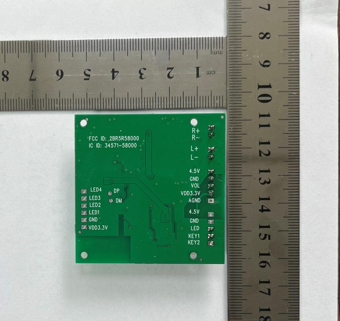
Click to zoom
Application Details
- Equipment Class
- DTS - Digital Transmission System
- Date of Grant
- May 22, 2026
- Application Purpose
- Original Equipment
- Equipment Note
- Module
- Frequency Range
- 2402.00000000 - 2480.00000000
- Company
- LIC LIMITED
- Country
- China
Documents & Files
Document Text
Text extracted from the exhibit documents filed with the FCC. Open a document above to read the original.
Users Manual
1 AC6956C Datasheet Version:1.1 Date:2026.05.11 AC6956C Datasheet 2 AC6956C Features CPU 32-bit DSP supports hardware Float Point Unit(FPU) Up to 240MHz programmable processor 64Vectored interrupts 4 Levels interrupt priority DSP Audio Processing SBC, AAC Audio decodes supported for BT audio mSBC voice codecs supported for BT phone Supports MP2, MP3, WMA, APE, FLAC, AAC, MP4, M4A, WAV, AIF, AIFC audio decoding Packet Loss Concealment (PLC) for voice processing Acoustic echo cancellation/suppression (AEC,AES) Single/Dual MIC Environmental Noise Cancellation (ENC) Multi-band DRC limiter 30-band EQ configuration for voice Effects Audio Codec Two channels 16-bit DAC, SNR >= 95dB Three channels 16-bit ADC , SNR >= 90dB Sampling rates of 8KHz/11.025KHz/16KHz/22.05KHz/24KHz/ 32KHz/44.1KHz/48KHz are supported One analog MIC amplifier, build-in MIC bias generator Supports two PDM digital MIC inputs three channels Stereo analog MUX Supports cap-less, single-ended, and differential mode at the DAC path Supports 16ohm and 32ohm Speaker loading Bluetooth Compliant with Bluetooth V5.1+BR+EDR+BLE specification Meet class1 class2 and class3 transmitting power requirement Provides +6dbm transmitting power receiver with -90dBm sensitivity Fast AGC for enhanced dynamic range Supports a2dp\avctp\avdtp\avrcp\hfp\spp\smp\att\gap\g att\rfcomm\sdp\l2cap profile Peripherals One full speed USB 2.0 OTG controller Four multi-function 16-bit timers, support capture and PWM mode Three 16-bit PWM generator for motor driving Three full-duplex basic UART, UART0 and UART1 supports DMA mode Two SPI interface supports host and device mode One hardware IIC interface supports host and device mode Built-in Cap Sense Key controller 10-bit ADC for analog sampling External wake up/interrupt on all GPIOs PMU Low voltage LDO for internal digital and analog circuit supply 3uA current consumption in the soft-off mode Built-in LDO for the core, I/O, Bluetooth and flash VBAT is 2.2V to 5.5V VDDIO is 2.2V to 3.6V Packages QFN32(4mm*4mm) AC6956C Datasheet 2 Temperature Operating temperature: -20°C to +70°C Storage temperature: -65°C to +150°C Applications Bluetooth Stereo Sound Box Bluetooth Mono Sound Box Bluetooth TWS Sound Box AC6956C Datasheet 2 1、Pin Definition 1.1 Pin Assignment 1 2 3 4 5 6 7 8 9 1011121314 1516 17 18 19 20 21 22 23 24 32 31 30 29 28 27 26 25 PB8 BT_AVDD VBAT DACL USBDM PA0 PB0PB3PB2 VDDIODACVSSMIC AC6956C (QFN32) GND BOM VCOMUSBDP DACR PC3 PC5 PC4 BT_OSCI PB1 LDO_IN/PB5 FMIP BT_OSC0 PA10PA9PA1 BT_RF PB9 PB11 PB10 PC7 PC2 Figure 1-1 AC6956C Package Diagram AC6956C Datasheet 3 1.2 Pin Description Table 1-1 AC6956C Pin Description PIN NO. Name I/O Type Drive (mA) Function Other Function 1 VCOM P / DAC Reference 2 DACL O / DAC Left Channel 3 DACR O / DAC Right Channel 4 FMIP I / FM Single Input 5 PB11 I/O / GPIO SDPG:SDC Power Gate; SPDIF_OUT:Sony/Philips Digital Interface Out 6 PB10 I/O 8/24 GPIO AMUX2R:Analog Channel2 Right; SPI2DOA:SPI2 Data Out(A); ADC9:ADC Input Channel 9; UART2RXC:Uart2 Data In(C); PWMCH3L:Motor PWM Channel3(L); 7 PB9 I/O 8/24 GPIO AMUX2L:Analog Channel2 Left; SPI2CLKA:SPI2 Clk(A); CAP0:Timer0 Capture; UART2TXC:Uart2 Data Out(C); PWMCH3H:Motor PWM Channel3(H); 8 PB8 I/O 8/24 GPIO AMUX1R:Analog Channel1 Right; SPI2_DIA:SPI2 Data In(A); ADC8:ADC Input Channel 8; CLKOUT1:Clk Out1; 9 LDO_IN P / Battery Charge Input PB5 I/O 8 GPIO (High Voltage Resistance) PWM3:Timer3 PWM Output; CAP1:Timer1 Capture; UART0TXC:Uart0 Data Out(C); UART0RXC:Uart0 Data In(C); 10 VBAT P / Power Supply 11 BT_AVDD P / BT Power 12 PB3 I/O 8/24 GPIO PWM2:Timer2 PWM Output; ADC6:ADC Input Channel 6; 13 PB2 I/O 8 GPIO (High Voltage Resistance) SPI1DIA:SPI1 Data In(A); PWMCH1L:Motor PWM Channel1 (L); 14 PB1 I/O 8/24 GPIO (pull up) Long Press Reset; SPI1DOA:SPI1 Data Out(A); AC6956C Datasheet 4 ADC5:ADC Input Channel 5; TMR2:Timer2 Clock Input; UART1RXA:Uart1 Data In(A); 15 PB0 I/O 8 GPIO (High Voltage Resistance) SPI1CLKA:SPI1 Clock(A); UART1TXA:Uart1 Data Out(A); PWMCH1H:Motor PWM Channel1(H); 16 BT_RF / / BT Antenna 17 BT_OSCI I / OSC In 18 BT_OSCO O / OSC Out 19 PC5 I/O 8/24 GPIO SD1CLKA:SD1 Clock(A); SPI1DOB:SPI1 Data Out(B); UART2RXD:Uart2 Data In(D); IIC_SDA_B:IIC SDA(B); ADC13:ADC Input Channel 13; PWMCH5L:Motor PWM Channel5(L); 20 PC4 I/O 8/24 GPIO SD1CMDA:SD1 Command(A); SPI1CLKB:SPI1 Clock(B); UART2TXD:Uart2 Data Out(D); IIC_SCL_B:IIC SCL(B); ADC10:ADC Input Channel 10; PWMCH5H:Motor PWM Channel5(H); 21 PC3 I/O 8/24 GPIO SD1DAT0A:SD1 Data0(A); SPI1DIB:SPI1 Data In(B); 22 PC2 I/O 8/24 GPIO SD1DAT1A:SD1 Data1(A); ALNK1_DAT0: Audio Link Data0; Touch12:Touch Input Channel 12; FPIN5:Motor Auto-Stop Protective Pin5; 23 USBDM I/O 4 USB Negative Data (pull down) UART1RXD:Uart1 Data In(D); IIC_SDA_A:IIC SDA(A); 24 USBDP I/O 4 USB Positive Data (pull down) UART1TXD:Uart1 Data Out(D); IIC_SCL_A:IIC SCL(A); ADC12:ADC Input Channel 12; 25 PA10 I/O 8/24 GPIO SD0CLKA:SD0 Clock(A); ALNK0_LRCKB:Audio Link Word Select(B); ADC3:ADC Input Channel 3; SPDIF_IN_B: Sony/Philips Digital Interface Input(B) TMR1:Timer1 Clock Input; Touch9:Touch Input Channel 9; UART2RXB:Uart2 Data In(B); PWMCH4L:Motor PWM Channel4(L); 26 PA9 I/O 8/24 GPIO SD0CMA:SD0 Command(A); AC6956C Datasheet 5 ALNK0_SCLKB:Audio Link Serial Clock(B); SPDIF_IN_A:Sony/Philips Digital Interface Input(A) Touch8:Touch Input Channel 8; UART2TXB:Uart2 Data Out(B); PWMCH4H:Motor PWM Channel4(H); 27 PA1 I/O 8/24 GPIO AMUX0R:Analog Channel0 Right; Touch1:Touch Input Channel 1; ADC0:ADC Input Channel 0; UART1RXC:Uart1 Data In(C); PWMCH0L:Motor PWM Channel0(L); 28 PA0 I/O 8/24 GPIO AMUX0L:Analog Channel0 Left; Touch0:Touch Input Channel 0; CLKOUT0: UART1TXC:Uart1 Data Out(C); PWMCH0H:Motor PWM Channel0(H); 29 PC7 I/O / GPIO MIC_BIAS:Microphone Bias Output 30 MIC I / MIC:MIC Input Channel; 31 VDDIO P / IO Power 3.3v 32 DACVSS P / DAC Ground AC6956C Datasheet 6 2、Electrical Characteristics 2.1 Absolute Maximum Ratings Ta b l e 2-1 Symbol Parameter Min Max Unit Tamb Ambient Temperature -20 …
Text truncated - open the document above for the full version.
Attestation Statements
LIC LIMITED Covered Equipment Certification Attestation Letter 12/8/2025 Nemko North America, Inc. 303 River Road Ottawa K1V 1H2 Canada ATTN.: Reviewing Engineer FCC ID: 2BR5R58000 LIC LIMITED certifies that the equipment for which authorization is sought is not “covered” equipment prohibited from receiving an equipment authorization pursuant to section 2.903 of the FCC rules. Note: If the equipment for which the applicant seeks authorization is produced by any of the entities identified on the current Covered List, the applicant should include an explanation on why the equipment is not “covered” equipment. LIC LIMITED certifies that, as of the date of the filing of the application, the applicant is not identified on the Covered List as an entity producing “covered” equipment. LIC LIMITED certifies that the equipment for which authorization is sought does not include cybersecurity or anti-virus software produced or provided by Kaspersky Lab, Inc. or any of its successors and assignees, including equipment with integrated Kaspersky Lab, Inc. (or any of its successors and assignees) cybersecurity oranti-virus software pursuant to DA-24-886 and KDB 986446 D01 Covered Equipment Guidance section B(2a). Signed: Printed name: Catherine Cheng Title: Merchandiser Company Name: LIC LIMITED Date: 12/8/2025
Attestation Statements
LIC LIMITED * the applicant must designate a contact located in the United States for purposes of acting as the applicant’s agent for service of process, regardless of whether the applicant is a domestic or foreign entity. An applicant located in the United States may designate itself as the agent for service of process. U.S. Agent Designation for Service of Process - Certification Attestation Letter DATE Nemko North America, Inc. 303 River Road Ottawa K1V 1H2 Canada ATTN.: Reviewing Engineer FCC ID: 2BR5R58000 Per section 2.911(d)(7) of the FCC rules, LIC LIMITED (“the applicant”) certifies that the equipment for which authorization is sought is designated to the following U.S. agent* for service of process: Company Name: LEMAX, Inc. Physical U.S. Company Address: 25 Pequot Way, Canton, MA 02021, United States. Agent name: Fernando Pacheco Agent Email Address: [email protected] FRN: 0037757663 The above contact person accepts the obligation for service of process. The applicant accepts to maintain an agent for no less than one year after the grantee has terminated all marketing and importation or the conclusion of any Commission-related proceeding involving the equipment. Applicant Signed: Agent Signed (if different to Applicant): Signed: Signed: Printed name: CATHERINE CHENG Printed name: Fernando Pacheco Title: MERCHANDISER Title: General Manager Company Name: LIC LIMITED Company Name: Lemax Inc. Date: 12/8/2025 Date: 12/17/2025 FRN: 0037492444
Block Diagram
<Drawn By> <Checked By> <QC By> <Released By> <Drawn Date> <Checked Date> <QC Date> <Release Date> <Company Name> <Title> <Code> B <Drawing Number> <Revision> <Scale> 1 1 REV: SIZE: CODE: DRAWN: DATED: DATED: CHECKED: QUALITY CONTROL: DATED: DATED: RELEASED: COMPANY: TITLE: DRAWING NO: SHEET: OF SCALE: REVISION RECORD APPROVED: ECO NO: A B D DATE: 1 2 3 4 5 6 D C A B C LTR LED KEY ASC6956C DC4.5V 25Q32 ANT CS8389 SPKL SPKR OSC FLASH 24MHZ
Cover Letter(s)
LIC LIMITED Date (2025-11-26) Federal Communications Commission Equipment Authorization Branch 7435 Oakland Mills Road Columbia, MD 21046 Modular Approval Request FCC ID: 2BR5R58000 The following attestation addresses the requirements to support modular approval: Modular approval requirement Yes (provide brief statement) No * (a) The radio elements must have the radio frequency circuitry shielded. Physical components and tuning capacitor(s) may be located external to the shield, but must be on the module assembly Yes: both side shielded (b) The module must have buffered modulation/data inputs to ensure that the device will comply with Part 15 requirements with any type of input signal Yes: All inputs to the modules are buffered through logic or microprocessor inputs. (c) The module must contain power supply regulation on the module Yes: A low drop out regulator is used for modular power supply regulation. (d) The module must contain a permanently attached antenna, or contain a unique antenna connector, and be marketed and operated only with specific antenna(s), per Sections 15.203, 15.204(b), 15.204(c), 15.212(a), 2.929(b) Yes: Device is equipped with PCB antenna. (e) The module must demonstrate compliance in a stand-alone configuration Yes: Stand-alone test method (f) The module must be labelled with its permanently affixed FCC ID label, or use an electronic display (See KDB Publication 784748 about labelling requirements) Yes: The modular has a permanent fixed label, and below statement was listed in the Users Manual; The host device must be labelled to display the FCC ID of the module Contains FCC ID: 2BR5R58000 (g) The module must comply with all specific rules applicable to the transmitter. The grantee must provide comprehensive instructions to explain compliance requirements Yes: The module comply with all specific rules applicable to the transmitter including all the conditions provided in the integration instructions by the grantee, Refer to test report and user manual . Modular approval requirement Yes (provide brief statement) No * (h) The module must comply with RF exposure requirements Yes: Transmitter meets MPE calculation of 47 CFR 1.1307 . Refer to MPE Reports and Refer to modular installation manual * Please provide a detailed explanation if the answer is “No.” Sincerely, Signed: Printed name: CATHERINE CHENG Title: MERCHANDISER
Operational Description
1.Radio Frequency Module Circuit Board Section An external power supply provides DC 4.5V voltage to the circuit board. Matchin g Networ k — This matchin g networ k alig ns the ant enna impedan ce with the impedanc e of the chipset RF module and provides filteri ng functio ns in the R F path. Antenna — A transceiver antenna interfaced with the IC via an L-C matching filter. It receives and transmits the modulated 2.4GHz RF signal through the air. Antenna gain: 2.92 dBi. Modulation Types: GFSK Bluetoot h: AC695N_soundbox_sdk_release_3.1.0 24MHz Crystal Oscillator — Serves as an external component interfaced with the IC, providing the reference clock source required for internal operations. Music playback is achieved by connecting via the antenna to external Bluetooth devices such as mobile phones and computers. Using an external Bluetooth function button, users can switch between Bluetooth music playback mode and internal music playback mode.
RF Exposure Info
DEKRA Testing and Certification (Shanghai) Ltd. Guangzhou Branch Block 5, No.3, Qiyun Road, Huangpu District, Guangzhou, Guangdong, China Tel +86 20 6661 2000 Fax +86 20 6661 2001 https://www.dekra.com Report no.: 4937111.58 Page 1 / 9 Test report No: 4937111.58 TEST REPORT Radio Spectrum Matters (RF) Identification of item tested Module Trademark LEMAX Model and /or type reference AC6956C FCC ID 2BR5R58000 Features 3 Vdc Applicant ́s name / address LIC LIMITED UNIT 3106, TOWER 1, ENTERPRISE SQUARE FIVE, NO. 38 WANG CHIU ROAD, KOWLOON BAY, KOWLOON, HONG KONG. Test method requested, standard KDB 447498 D01V06 FCC Part 1.1310 Verdict Summary COMPLIANCE Tested by (name & signature) Johnny Bo Approved by (name & signature) Tim Yan Date of issue 2026-01-05 Report template No TRF_EMC 2017-06- FCC_Exposure DEKRA Testing and Certification (Shanghai) Ltd. Guangzhou Branch Block 5, No.3, Qiyun Road, Huangpu District, Guangzhou, Guangdong, China Tel +86 20 6661 2000 Fax +86 20 6661 2001 https://www.dekra.com Report no.: 4937111.58 Page 2 / 9 INDEX page General conditions ...................................................................................................................................................... 3 Uncertainty .................................................................................................................................................................. 3 Environmental conditions............................................................................................................................................ 3 Possible test case verdicts ......................................................................................................................................... 3 Definition of symbols used in this test report .............................................................................................................. 4 Abbreviations .............................................................................................................................................................. 4 Document History ....................................................................................................................................................... 4 Remarks and Comments ............................................................................................................................................ 4 1 General Information ........................................................................................................................................... 5 1.1 General Description of the Item(s) .......................................................................................................... 5 1.2 Test data ................................................................................................................................................. 6 1.3 The environment(s) in which the EUT is intended to be used ................................................................ 6 2 Description of Test Setup .................................................................................................................................. 7 2.1 Operating mode(s) used for tests............................................................................................................ 7 2.2 Support / Auxiliary equipment / unit / software for the EUT .................................................................... 7 2.3 Test Configuration / Block diagram used for tests .................................................................................. 7 3 RF Exposure Evaluation .................................................................................................................................... 8 3.1 Limits ....................................................................................................................................................... 8 3.2 Test Procedure ........................................................................................................................................ 9 3.3 Test Result .............................................................................................................................................. 9 DEKRA Testing and Certification (Shanghai) Ltd. Guangzhou Branch Block 5, No.3, Qiyun Road, Huangpu District, Guangzhou, Guangdong, China Tel +86 20 6661 2000 Fax +86 20 6661 2001 https://www.dekra.com Report no.: 4937111.58 Page 3 / 9 GENERAL CONDITIONS 1. This report is only referred to the item that has undergone the test. 2. This report does not constitute or imply on its own an approval of the product by the Certification Bodies or Competent Authorities. 3. This document is only valid if complete; no partial reproduction can be made without previous written permission of DEKRA. 4. This test report cannot be used partially or in full for publicity and/or promotional purposes without previous written permission of DEKRA. 5. This report will not be used for social proof function in China market. UNCERTAINTY For all measurements where guidance for the calculation of the instrumentation uncertainty of a measurement is specified in EN 55016-4-2 (CISPR 16-4-2), EN/IEC 61000-4 series or a product standard, the measurement instrumentation uncertainty has been calculated and applied in accordance with these standards. Uncertainties have been calculated according to the DEKRA internal document. The reported expanded uncertainties are based on a standard uncertainty multiplied by a coverage factor of k=2, providing a level of confidence of approximately 95%. ENVIRONMENTAL CONDITIONS The climatic conditions during the tests are within the limits specified by the manufacturer for the operation of the EUT and the test equipment. The climatic conditions during the tests were within the following limits: Ambient temperature 15 °C – 35 °C Relative Humidity air 30% - 60% Atmospheric pressure 86 kPa – 106 kPa If explicitly required in the basi…
Text truncated - open the document above for the full version.
Schematics
C14104 C13104 C 1 7 1 0 5 C 1 0 2 . 7 p F C15105 13 4 2 Y1 24MHz R 2 1 0 R 1 V C O M 2 D A C L 3 D A C R 4 F M I P 5 P B 1 1 / S D _ P W R 6 P B 1 0 / S D 0 C M D / A D C 9 7 P B 9 / S D 0 C L K 8 P B 8 / S D 0 D A T / A D C 8 9 LDO_IN/PB5 10 VBAT 11 BT_AVDD 12 PB3/PR1/ADC6 13 PB2/PR0 14 PB1/ADC5 15 PB0 16 BT_RF 1 7 B T _ O S C I 1 8 B T _ O S C O 1 9 P C 5 / S D 1 C L K / A D C 1 3 2 0 P C 4 / S D 1 C M D / A D C 1 0 2 1 P C 3 / S D 1 D A T 2 2 P C 2 2 3 U S B D M / P A 1 2 / A D C 4 2 4 U S B D P / A D C 1 2 25 PA10/ADC3 26 PA9 27 PA1/AUX0R/ADC0 28 PA0/AUX0L 29 PC7/MIC_BIAS 30 MIC 31 VDDIO 32 DACVSS 33 GND U 1 A C 6 9 5 6 C C 1 6 1 0 5 C1105 C2105 12 S P 2 1 2 A N T 1 D M D P 16 15 14 13 12 11 10 98 7 6 5 4 3 2 1 U2 CS8389 C3105 C4105 12 S P 1 1 2 3 4 5 6 CTRL2 12345 C T R L 5 12345 C T R L 3 C 4 1 4 7 0 u F 1 0 V C36104 1234 5678 U 3 2 5 Q 3 2 L 1 4 . 7 U H C 6 4 7 0 u F 1 0 V C35104 12 D1 SS34 C26 104 C37 105 C 3 9 4 7 0 u F 1 0 V R27 1R C8 106 L2 10UH L3 10UH L4 10UH L5 10UH C25104 C 4 0 4 7 0 u F 1 0 V R 2 0 7 5 K C 2 7 1 0 3 R922 8.2K C21224 R16 10K R1922 10K R15 8.2K R17 8.2K R8 8.2K C29224 C31224 C20224 C23NC C22NC R 5 1 K R 6 1 K C 1 8 1 0 5 C 1 9 1 0 5 R 1 1 0 0 R C 5 1 0 4 C28104 R11NC R12NC R13NC R14NC R 7 0 R C30 NC R 1 0 0 R C33NC R 2 3 0 R R 2 6 N C R 2 5 N C R 3 1 0 0 R C34 NC R 2 2 0 R C9 NC R 2 4 0 R C38 NC R 4 0 R C12NC C11NC R 1 8 5 . 1 R C 3 2 1 0 3 1 2 K 1 C7105 L 3.3V S D - P W R D A T - S P I L E D B 1234 MUTE L+ L- R- R+ L + L - R + R - M U T E LR R D A T - S P I C M D - S P I S D - P W R C M D - S P I C L K - S P I C L K - S P I D1 D2 D3 D4 D 4 D 3 D 2 D 1 3 . 3 V 3 . 3 V V + - 1 2 3 4 L E D B K E Y 1 KEY2 KEY2 KEY1 V+- 4 . 5 V 4 . 5 V K E Y 1
Test Report
DEKRA Testing and Certification (Shanghai) Ltd. Guangzhou Branch Block 5, No.3, Qiyun Road, Huangpu District, Guangzhou, Guangdong, China Tel +86 20 6661 2000 Fax +86 20 6661 2001 https://www.dekra.com Report no.: 4937111.56 Page 1 / 53 Test report No: 4937111.56 TEST REPORT Radio Spectrum Matters (RF) Identification of item tested Module Trademark LEMAX Model and /or type reference AC6956C FCC ID 2BR5R58000 Features 3 Vdc Applicant ́s name / address LIC LIMITED UNIT 3106, TOWER 1, ENTERPRISE SQUARE FIVE, NO. 38 WANG CHIU ROAD, KOWLOON BAY, KOWLOON, HONG KONG. Test method requested, standard FCC CFR Title 47 Part15 Subpart C Section 15.247; KDB558074 D01v05r02; Verdict Summary COMPLIANCE Tested by (name & signature) Johnny Bo Approved by (name & signature) Tim Yan Date of issue 2026-01-05 Report template No TRF_EMC 2017-06- FCC_Part15C_247 DEKRA Testing and Certification (Shanghai) Ltd. Guangzhou Branch Block 5, No.3, Qiyun Road, Huangpu District, Guangzhou, Guangdong, China Tel +86 20 6661 2000 Fax +86 20 6661 2001 https://www.dekra.com Report no.: 4937111.56 Page 2 / 53 INDEX page General conditions ...................................................................................................................................................... 4 Uncertainty .................................................................................................................................................................. 4 Environmental conditions............................................................................................................................................ 4 Possible test case verdicts ......................................................................................................................................... 4 Definition of symbols used in this test report .............................................................................................................. 5 Abbreviations .............................................................................................................................................................. 5 Document History ....................................................................................................................................................... 5 Remarks and Comments ............................................................................................................................................ 5 1 General Information ........................................................................................................................................... 6 1.1 General Description of the Item(s) .......................................................................................................... 6 1.2 Test data ................................................................................................................................................. 7 1.3 The environment(s) in which the EUT is intended to be used ................................................................ 7 1.4 Channel List ............................................................................................................................................ 8 2 Description of Test Setup .................................................................................................................................. 9 2.1 Operating mode(s) used for tests............................................................................................................ 9 2.2 Support / Auxiliary equipment / unit / software for the EUT .................................................................... 9 2.3 Test Configuration / Block diagram used for tests .................................................................................. 9 2.4 Measurement procedure ....................................................................................................................... 10 3 Verdict summary section ................................................................................................................................. 11 3.1 Standards .............................................................................................................................................. 11 3.2 Deviation(s) from the Standard(s) / Test Specification(s) ..................................................................... 11 3.3 Overview of results ................................................................................................................................ 11 4 Transmitter Test Results ................................................................................................................................. 12 4.1 AC Power Line Conducted Emission .................................................................................................... 12 4.2 Emissions in non-restricted frequency bands ....................................................................................... 15 4.3 Emissions in restricted frequency bands .............................................................................................. 26 4.4 Band Edge ............................................................................................................................................. 33 4.5 Duty cycle .............................................................................................................................................. 36 4.6 DTS Bandwidth ..................................................................................................................................... 38 4.7 Fundamental emission output power .................................................................................................... 43 4.8 Power Density ....................................................................................................................................... 46 5 Identification of the Equipment Under Test ........................................…
Text truncated - open the document above for the full version.
Test Report
2.4G-2.48G频段板载PIFA天线测试报告 2.4G-2.48GInvertedFAntennaSpecification SPECIFICATIONS Frequency(MHz)2400-2480 PeakGain(dBi)2.92 AverageGain(dBi)1.08 VSWR<1.6 Impedance(Ω)50Ω AntennaTypePlannarInvertedFAntennaonboard PolarizationLinear ManufactureZHUHAIJIELITECHNOLOGYCO.,LTD Address: No.333KexingRoad,NanpingSciencePark,XiangzhouDistrict, Zhuhai TestequipmentHWA-TECH AntennaPhoto&Length(mm) 天线无源S参数: AntennapassiveS-parameters: 驻波比( VSWR )、回波损耗( ReturnLoss )及史密斯圆图( Smith ) 天线效率及增益: Antennaefficiencyandgain : Frequency(MHz)Gain(dBi)Effciency(%)AverageGain(dBi)Efficiency(dB) 24002.9272.20%-1.14-1.41 24101.9561.36%-2.05-2.12 24202.0061.00%-1.98-2.15 24300.8047.29%-3.09-3.25 24400.1240.82%-3.87-3.89 24500.9748.41%-3.08-3.15 24601.2853.80%-2.81-2.69 24701.2951.75%-2.98-2.86 24801.7958.79%-2.45-2.31 Average1.4655.05%-2.61-2.65 Peak2.9272.20%-1.14-1.41 天线2440MHz2D-ThetaPattern 天线2440MHz2D-PhiPattern 天线2440MHz3D-TotalPattern
Test Setup Photos
Radiated emissions Radiated emissions (above 1GHz) Conducted emission
Contact Information
Applicant
CATHERINE CHENG
[email protected]Fax: +852 23114646
Technical Contact
LEMAX, Inc.Fernando Pacheco
25 Pequot Way, Canton, MA 02021, U.S.A. · Canton, Maine, 02021 · United States
Test Firm
DEKRA Testing and Certification (Shanghai) Ltd.Johnson Liu
Technical Specifications
| # | Rule Parts | Frequency Range | Power Output |
|---|---|---|---|
| 1 | 15C | 2.40 GHz - 2.48 GHz | 580.00 µW |