2BRUZ-AR4aaboRing 4
1008 Digital Health Pvt. Ltd.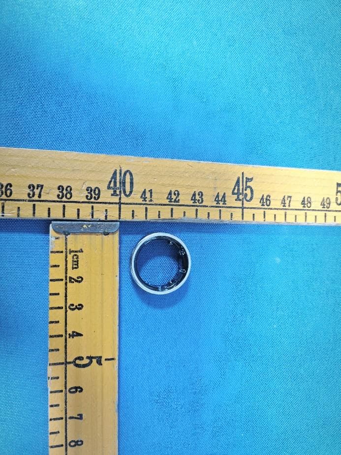
Click to zoom
Application Details
- Equipment Class
- DTS - Digital Transmission System
- Date of Grant
- Sep 30, 2025
- Application Purpose
- Original Equipment
- Equipment Note
- aaboRing 4
- Frequency Range
- 2402.00000000 - 2480.00000000
- Country
- India
Documents & Files
Document Text
Text extracted from the exhibit documents filed with the FCC. Open a document above to read the original.
Users Manual
Setup Guide Charge for 60 - 180 minutes Charge the Ring Plug USB to Power Adapter, Green LED light will blink while charging & it will remain solid green when fully charged Keep the Ring in Charging Case till it is Bound with aaboRing® App Download aaboRing® App Login aaboRing ® App aaboRing ® aaboRing ® Your cir cle of healt h xxx-xxx-xxxx Bind Ring with app Ring must b e in th e charg ing case aaboRing 4_5B7B F 1:76:65:58:5B:7B Silver, Size 10 Note: The unbound Ring will only broadcast w hen charging, please charge it so that the app can scan it. APP can scan it. 1. Ensure aaboRing is connected to charging case. 2. Check aaboRing is fully charged. 3. If aaboRing was connected to other phone/app then logout from the app. 4. In this case aaboRing will be required to factory reset. 218-250738 The product is too small to be engraved. Wear Ensure sensors touch palm side of finger Check your mindfulness now All Set! ® Anytime, Anywhere! Data capturing starts within 30 mins Experience aaboRing aaboRing aaboRing Your circle of health aaboRing Your circle of health FC C Cau tion . This device complies with part 15 of the FCC Rules. Operation is subject to the following two conditions: (1) This device may not cause harmful interference, and (2) this device must accept any interference received, including interference that may cause undesired operation. Any Changes or modifications not expressly approved by the party responsible for compliance could void the user's auth ority to operate the equipment. Note: This equipment has been tested and found to comply with the limits for a Class B digital device, pursuant to part 15 of the FCC Rules. These limits are designed to provide reasonable protection against harmful interference in a residential installation. This equipment generates uses and can radiate radio frequency energy and, if not in stalled and used in accordance w ith the instructions, may cause harmful interference to radio communications. However, there is no guara ntee that interference will not occur in a particular installation. If this equipment does cause harmful interference to radio or television reception, which can be determined by turning the equipment off and on, the user is encouraged to try to correct the interference by one or more of the following measures: -Reorient or relocate the receiving antenna. -Increase the separa tion between the equipment and receiver. -Connect the equipment into an outlet on a circuit different from that to which the receiver is connected. -Consult the dealer or an experienced radio /TV technician for help. *R F w arning for Portable device: The device has been evaluated to meet general RF exposure requirement. The device c an be used in portable exposure condition without restriction. Enter the circle of health & wellness aarrooggaa bohilabhaam Good Health for All aabo® & aaboRing® are registered trademarks of 1008 Digital Health Pvt. Ltd. India
Attestation Statements
1008DigitalHealthPvt.Ltd. CoveredEquipmentCertificationAttestationLetter 9/18/2025 NemkoNorthAmerica,Inc. 303RiverRoad Ottawa K1V1H2 Canada ATTN.:ReviewingEngineer FCCID:2BRUZ-AR4 1008DigitalHealthPvt.Ltd.(“theapplicant”)certifiesthattheequipmentforwhich authorizationissoughtisnot“covered”equipmentprohibitedfromreceivingan equipmentauthorizationpursuanttosection2.903oftheFCCrules. Note:Iftheequipmentforwhichtheapplicantseeksauthorizationisproducedby anyoftheentitiesidentifiedonthecurrentCoveredList,theapplicantshould includeanexplanationonwhytheequipmentisnot“covered”equipment. 1008DigitalHealthPvt.Ltd.(“theapplicant”)certifiesthat,asofthedateofthefilingof theapplication,theapplicantisnotidentifiedontheCoveredListasanentityproducing “covered”equipment. 1008DigitalHealthPvt.Ltd.(“theapplicant”)certifiesthattheequipmentforwhich authorizationissoughtdoesnotincludecybersecurityoranti-virussoftwareproducedor providedbyKasperskyLab,Inc.oranyofitssuccessorsandassignees,including equipmentwithintegratedKasperskyLab,Inc.(oranyofitssuccessorsandassignees) cybersecurityoranti-virussoftwarepursuanttoDA-24-886andKDB986446D01 CoveredEquipmentGuidancesectionB(2a). Signed: Printedname:AtulHemani Title:Co-Founder CompanyName:1008DigitalHealthPvt.Ltd. Date:9/18/2025
Cover Letter(s)
1008DigitalHealthPvt.Ltd. 9/19/2025 NemkoNorthAmerica,Inc. 303RiverRoad Ottawa,Ontario,Canada K1V1H2 REQUESTFORCONFIDENTIALITY-FCC FCCID:2BRUZ-AR4 PursuanttoSections0.457(d)(1)(ii)and0.459oftheCommission’sRulesandFCCGuidance document726920,weherebyrequestconfidentialtreatmentofinformationaccompanyingthis applicationasoutlinedbelow: PERMANENTLONG-TERMCONFIDENTIALITY: Schematics BlockDiagrams TheoryofOperation Theaboveinformationcontainstradesecretsandproprietaryinformationnotcustomarilyreleasedto thepublic.Thepublicdisclosureofthisinformationmightbeharmfultotheapplicantandprovide unjustifiedbenefitstoitscompetitors.TheApplicantunderstandsthatpursuanttoRule0.457(d)(1)(ii), disclosureofthisApplicationandallaccompanyingmaterialswillnotbemadebeforethedateofthe GrantforthisApplication. Sincerely, Signed: Printedname:AtulHemani Title:Co-Founder
Cover Letter(s)
1008DigitalHealthPvt.Ltd. FamilyCertificationAttestationLetter 9/18/2025 NemkoCanadaInc 303RiverRoad Ottawa K1V1H2 Canada ATTN.:ReviewingEngineer ProductName:aaboRing4 Models:AR4,AR4X,AR4P,AR4Z,AR4XZ FCCID:2BRUZ-AR4 Weherebystatethatallthemodelsareelectricalidenticalincludingthesamesoftware parameterandhardwaredesign(i.e.,circuitdesign,PCBlayout,RFmodule/circuit, antennatype(s)andantennalocation,componentsonPCB,etc.,),samemechanical structureanddesign(includingproductenclosure,materials,etc.,). AR4XisanupgradedversionofAR4,featuringa20daysbatterylife AR4PisanextendedversionofAR4,equippingthechargingcaseofAR4withthe environmentsensingfunction. AR4ZisanupgradedversionofAR4,featuringtheAIalgorithms. AR4XZisanupgradedversionofAR4,featuringtheAIalgorithmsanda20daysbattery life. Signed: Printedname:AtulHemani Title:Co-Founder Date:9/18/2025
External Photos
FCC ID: 2BRUZ-AR4 FCC ID: 2BRUZ-AR4 FCC ID: 2BRUZ-AR4
ID Label/Location Info
LabelandLabelLocation Theproductistoosmalltobeengraved. TheFCCIDandMIClogoistypedontheusermanualandontheproductpackag. Packagphoto:
Internal Photos
FCC ID: 2BRUZ-AR4 FCC ID: 2BRUZ-AR4 Ant
RF Exposure Info
Page1of2 RFEXPOSUREEVALUATION FCCID:2BRUZ-AR4 Modeldifference: AR4isandowngradedversionofAR4XZ,withoutthefeatureoftheAIalgorithmsand thefeatureof20daysbatterylife. AR4XisandowngradedversionofAR4XZ,withoutthefeatureoftheAIalgorithms. AR4PisanextendedversionofAR4XZ,equippingthechargingcaseofAR4withthe environmentsensingfunction. AR4ZisandowngradedversionofAR4XZ,withoutthefeatureof20daysbatterylife. ProductName: aaboRing4 ModelName: AR4XZ,AR4,AR4X,AR4P,AR4Z BluetoothVersion:BT5.1 Operatingfrequency:2402-2480MHz NumbersofChannel:40channelsForDTS AntennaType:Ceramicantenna AntennaGain:2.28dBi TypeofModulation:GFSK Powersupply: Input:DC5VA Li-ionBattery:170724 Voltage:3.7V Capacity:16.5mAh0.0611Wh Theringischargedwirelessly HardwareVersion:V1.0 SoftwareVersion:V1.0 Page2of2 StandardRequirement Accordingto§15.247(i)and§1.1307b(1),systemsoperatingundertheprovisionsofthis sectionshallbeoperatedinamannerthatensuresthatthepublicisnotexposedtoradio frequencyenergylevelsinexcessoftheCommission’sguidelines.SeeKDB447498D01 GeneralRFExposureGuidancev06,section4.3.1. The1-gand10-gSARtestexclusionthresholdsfor100MHzto6GHzattestseparation distances≤50mmaredeterminedby: [(max.powerofchannel,includingtune-uptolerance,mW)/(min.testseparationdistance, mm)]*[√f(GHz)]≤3.0for1-gSARand≤7.5for10-gSARextremitySAR,where f(GHz)istheRFchanneltransmitfrequencyinGHz PoweranddistanceareroundedtothenearestmWandmmbeforecalculation Theresultisroundedtoonedecimalplaceforcomparison. Thetestexclusionsareapplicableonlywhentheminimumtestseparationdistanceis≤ 50mmandfortransmissionfrequenciesbetween100MHzand6GHz.Whentheminimumtest separationdistanceis<5mm,adistanceof5mmisappliedtodetermineSARtestexclusion. RoutineSARevaluationreferstothatspecificallyrequiredby§2.1093,usingmeasurements orcomputersimulation.WhenroutineSARevaluationisnotrequired,portabletransmitters withoutputpowergreaterthantheapplicablelowthresholdrequireSARevaluationtoquality forTCBapproval. Channel (MHz) Maximum output power (dBm) Tuneup tolerance (dBm) MaxTune UpPower (mW) Distance (mm) Calculation results Limit Operating Mode 24021.181.18±11.65196250.5120553BLE AccordingtoKDB447498,ThedeviceonlysupportBTfunction,andnosimultaneousSAR measurementisrequired. Signature SimonPu Manager Date:2025-09-28
Test Report
Page1of69 FCCTESTREPORT FCCID:2BRUZ-AR4 Product: aaboRing4 ModelName: AR4XZ,AR4,AR4X,AR4P,AR4Z Brand: aabo ReportNo.: PTC25080600101E-FC01 Preparedfor 1008DigitalHealthPvt.Ltd. 401/402,Giriraj,NilkanthValley,Rajawadiroad.No.7,GhatkoparEast,Mumbai-400077India Preparedby PreciseTesting&CertificationCo.,Ltd Building1,No.6,TongxinRoad,DongchengStreet,Dongguan,Guangdong,China ReportNo.:PTC25080600101E-FC01 Page2of69 1TESTRESULTCERTIFICATION Applicant’sname:1008DigitalHealthPvt.Ltd. Address: 401/402,Giriraj,NilkanthValley,Rajawadiroad.No.7,GhatkoparEast, Mumbai-400077India Manufacture'sname:1008DigitalHealthPvt.Ltd. Address: 401/402,Giriraj,NilkanthValley,Rajawadiroad.No.7,GhatkoparEast, Mumbai-400077India Productname:aaboRing4 Modelname:AR4XZ,AR4,AR4X,AR4P,AR4Z Standards:FCCCFR47Part15Section15.247 Testprocedure:ANSIC63.10:2013 TestDate: Aug.18,2025toAug.24,2025 DateofIssue: Sep.28,2025 TestResult:Pass ThisdevicedescribedabovehasbeentestedbyPTC,andthetestresultsshowthatthe equipmentundertest(EUT)isincompliancewiththeFCCrequirements.Anditisapplicableonlyto thetestedsampleidentifiedinthereport. Thisreportshallnotbereproducedexceptinfull,withoutthewrittenapprovalofPTC,thisdocument maybealteredorrevisedbyPTC,personalonly,andshallbenotedintherevisionofthedocument. TestEngineer: Jackzhou/Engineer TechnicalManager: SimonPu/Manager ReportNo.:PTC25080600101E-FC01 Page3of69 Contents Page 1TESTRESULTCERTIFICATION...............................................................................................................................2 2TESTSUMMARY..........................................................................................................................................................5 2.1TESTSITE............................................................................................................................................................6 3GENERALINFORMATION.......................................................................................................................................7 3.1GENERALDESCRIPTIONOFE.U.T.....................................................................................................................7 3.2CHANNELLIST.....................................................................................................................................................8 4EQUIPMENTDURINGTEST....................................................................................................................................9 4.1EQUIPMENTSLIST.............................................................................................................................................9 4.2MEASUREMENTUNCERTAINTY.........................................................................................................................11 4.3DESCRIPTIONOFSUPPORTUNITS...................................................................................................................12 5CONDUCTEDEMISSION..........................................................................................................................................13 5.1E.U.T.OPERATION............................................................................................................................................13 5.2EUTSETUP.......................................................................................................................................................13 5.3TESTSET-UP(BLOCKDIAGRAMOFCONFIGURATION).................................................................................14 5.4MEASUREMENTPROCEDURE............................................................................................................................14 5.5CONDUCTEDEMISSIONLIMIT...........................................................................................................................14 5.6MEASUREMENTDESCRIPTION..........................................................................................................................14 5.7CONDUCTEDEMISSIONTESTRESULT.............................................................................................................14 6RADIATEDSPURIOUSEMISSIONS......................................................................................................................25 6.1EUTOPERATION...............................................................................................................................................25 6.2TESTSETUP......................................................................................................................................................26 6.3SPECTRUMANALYZERSETUP..........................................................................................................................27 6.4TESTPROCEDURE.............................................................................................................................................28 6.5SUMMARYOFTESTRESULTS...........................................................................................................................30 7CONDUCTBANDEDGEANDSPURIOUSEMISSIONSMEASUREMENT....................................................44 7.1TESTPROCEDURE.............................................................................................................................................44 7.2TESTSETUP......................................................................................................................................................44 7.3TESTRESULT....................................................................................................................................................45 ReportNo.:PTC25080600101E-FC01 Page4of69 86DBBANDWIDTHMEASUREMENT......................................................................................................................52 TESTPROCEDURE................................................................................................................…
Text truncated - open the document above for the full version.
Test Report
承 認 書 SPECIFICATION FOR APPROVAL 客戶名稱 CUSTOMER : 客戶料號 CUSTOMER’S P/N : 料號 PART NUMBER : WAN1608H245H08 規格 DESCRIPTION : Chip Antenna 1608 MH-Ant 2.45G Type H08 版本 VERSION : V1.0 日期 ISSUE DATE : 2021/03/03 客 戶 承 認 CUSTOMER APPROVED 工 程 部 R&D CENTER 承 認 APPROVAL 確 認 CHECKED 製 作 DRAWN Ray Tennyson Snow 萬誠科技股份有限公司 OneWave Electronic Co., Ltd. 112台北市北投區立功街151號1樓 1F, No. 151, Li Gong Street, Beitou District, Taipei City 112, Taiwan 電話: (02) 2898-2220 TEL: +886 2 2898-2220 傳真: (02) 2898-5055 FAX: +886 2 2898-5055 ONEWAVE TECHNOLOGY CO., LTD. 2/12 1608 Chip antenna For Bluetooth / WLAN Applications Dimension (mm) L 1.70 ± 0.20 W 0.93 ± 0.20 T 0.75 ± 0.20 P/N: WAN1608H245H08 ONEWAVE TECHNOLOGY CO., LTD. 3/12 Part Number Information WAN 1608 H 245 H 08 A B C D E F A Product Series Antenna B Dimension L x W 1.6X0.8mm (+-0.2mm) C Material High K material D Working Frequency 2.4 ~ 2.5GHz E Feeding mode Monopole & Single Feeding F Antenna type Type = 08 1. Electrical Specification Remark : Bandwidth & Peak Gain was measured under evaluation board of next page Specification Part Number WAN1608H245H08 Central Frequency 2450 MHz Bandwidth 120 (Min.) MHz Return Loss -10(Max) dB Peak Gain 2.28 dBi Impedance 50 Ohm Operating Temperature -40~+110 °C Maximum Power 4 W Resistance to Soldering Heats 10 ( @ 260°C) sec. Polarization Linear Azimuth Beamwidth Omni-directional Termination Cu / Sn (Leadless) ONEWAVE TECHNOLOGY CO., LTD. 4/12 2. Recommended PCB Pattern 1. Evaluation Board Dimension (若淨空區夠大,建議在天線尾段加Trace,效能更佳) Unit : mm 2. Evaluation Board Dimension (若淨空區夠大,建議在天線尾段加Trace,效能更佳) 3. Evaluation Board Dimension ONEWAVE TECHNOLOGY CO., LTD. 5/12 Suggested Matching Circuit 重要資訊 : 匹配元件建議使用精準度高的電感±0.1~0.3nH、電容±0.1pF 1. Layout Dimensions in Clearance area(Size=5.5*4mm) 50 ohm transmission Line Matching Circuit 2. Layout Dimensions in Clearance area(Size=5.5*4mm) 50 ohm transmission Line Matching Circuit 1~10nH None 0Ω 1.5pF ONEWAVE TECHNOLOGY CO., LTD. 6/12 3. Layout Dimensions in Clearance area(Size=5*3mm) 50 ohm transmission Line Matching Circuit FootPrint (Unit : mm) ONEWAVE TECHNOLOGY CO., LTD. 7/12 3. Measurement Results Return Loss ONEWAVE TECHNOLOGY CO., LTD. 8/12 Radiation Pattern Efficiency Peak Gain Directivity 2400MHz 50.65 % 1.80 dBi 3.95 dBi 2450MHz 53.27 % 2.28 dBi 4.42 dBi 2500MHz 50.32 % 1.77 dBi 4.15 dBi Chamber Coordinate System Y Z X ONEWAVE TECHNOLOGY CO., LTD. 9/12 4.Reliability and Test Condictions ITEM REQUIREMENTS TEST CONDITION Solderability 1. Wetting shall exceed 90% coverage 2. No visible mechanical damage Pre-heating temperature:150°C/60sec. Solder temperature:230±5°C Duration:4±1sec. Solder:Sn-Ag3.0-Cu0.5 Flux for lead free: rosin Solder heat Resistance 1. No visible mechanical damage 2. Central Freq. change :within ± 6% 10 ± 0.5 sec. 60 sec . . T E M P ( °C ) 150 °C 2 6 0 °C Pre-heating temperature:150°C/60sec. Solder temperature:260±5°C Duration:10±0.5sec. Solder:Sn-Ag3.0-Cu0.5 Flux for lead free: rosin Component Adhesion (Push test) 1. No visible mechanical damage The device should be reflow soldered(230±5°C for 10sec.) to a tinned copper substrate A dynometer force gauge should be applied the side of the component. The device must with-ST-F 0.5 Kg without failure of the termination attached to component. Component Adhesion (Pull test) 1. No visible mechanical damage Insert 10cm wire into the remaining open eye bend ,the ends of even wire lengths upward and wind together. Terminal shall not be remarkably damaged. Thermal shock 1. No visible mechanical damage 2. Central Freq. change :within ±6% Phase Temperature(°C) Time(min) 1 +110±5°C 30±3 2 Room Temperature Within 3sec 3 -40±2°C 30±3 4 Room Temperature Within 3sec +110°C=>30±3min -40°C=>30±3min Test cycle:10 cycles The chip shall be stabilized at normal condition for 2~3 hours before measuring. Resistance to High Temperature 1. No visible mechanical damage 2. Central Freq. change :within ±6% 3. No disconnection or short circuit. Temperature: +110±5°C Duration: 1000±12hrs The chip shall be stabilized at normal condition for 2~3 hours before measuring. Resistance to Low Temperature 1. No visible mechanical damage 2. Central Freq. change :within ±6% 3. No disconnection or short circuit. Temperature:-40±5°C Duration: 1000±12hrs The chip shall be stabilized at normal condition for 2~3 hours before measuring. Humidity 1. No visible mechanical damage 2. Central Freq. change :within ±6% 3. No disconnection or short circuit. Temperature: 40±2°C Humidity: 90% to 95% RH Duration: 1000±12hrs The chip shall be stabilized at normal condition for 2~3 hours before measuring. 4±1 sec. 60sec TEMP (°C) 150°C 230°C ONEWAVE TECHNOLOGY CO., LTD. 10/12 5.Soldering and Mounting Mildly activated rosin fluxes are preferred. The minimum amount of solder can lead to damage from the stresses caused by the difference in coefficients of expansion between solder, chip and substrate. The terminations are suitable for all wave and re-flow soldering systems. If hand soldering cannot be avoided, the preferred technique is the utilization of hot air soldering tools. Recommended temperature profiles for re-flow soldering in Figure 1. Products attachment with a soldering iron is discouraged due to the inherent process control limitations. In the event that a soldering iron must be employed the following precautions are recommended. ‧Preheat circuit and products to 150°C ‧Never contact the ceramic with the iron tip ‧Use a 20 watt soldering iron with tip diameter of 1.0mm ‧280°C tip temperature (max) ‧1.0mm tip diameter (max) ‧Limit soldering time to 3 sec. SOLDERING COOLING NATURAL PRE-HEATING TEMPERATURE(°C) 60~120 s 10s max. 30~60s 250~260 230 180 150 TIME(sec.) Reflow Soldering SOLDERING COOLING NATURAL PRE-HEATING TEMPERATURE(°C) within 3s Gradual cooling 150 TIME(sec.) Iron Soldering Over 60s 350 300 ONEWAVE TECHNOLOGY CO., LTD. 11/12 6.Packaging Information ◆ Tape Specification: W Ao Bo Ko P F E D D1 Po P2 t 8.0 ±0.30 1.10± 0.05 1.90 ±0.10 1.10± 0.10 4.00 ±0.05…
Text truncated - open the document above for the full version.
Test Setup Photos
FCC ID: 2BRUZ-AR4 Conducted Emissions Radiated Spurious Emissions From 30MHz-1000MHz FCC ID: 2BRUZ-AR4 Test frequency from Above 1GHz
Contact Information
Applicant
Atul Hemani(Co-Founder)
[email protected]Fax: +91 9321547875
Test Firm
Precise Testing & Certification Co., LTD.Yang Juan
Technical Specifications
| # | Rule Parts | Frequency Range | Power Output |
|---|---|---|---|
| 1 | 15C | 2.40 GHz - 2.48 GHz | 1.31 mW |