2BSDL-Z320Projector
Shenzhen Ouqing Technology Co., Ltd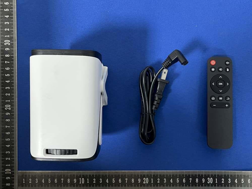
Click to zoom
Application Details
- Equipment Class
- DTS - Digital Transmission System
- Date of Grant
- Dec 04, 2025
- Application Purpose
- Original Equipment
- Equipment Note
- Projector
- Frequency Range
- 2412.00000000 - 2462.00000000
- Country
- China
Documents & Files
Document Text
Text extracted from the exhibit documents filed with the FCC. Open a document above to read the original.
Users Manual
User Manual (英语) Settings - Projector Settings, enter settings for projection mode, keystone correction, and scaling. This manual is for reference only. They are subject to change without prior notice. FCC Warning This equipment generates, uses and can radiate radio frequency energy and, if not installed and used in accordance with the instructions, may cause harmful interference to radio communications. However, there is no guarantee that interference will not occur in a particular installation. If this equipment does cause harmful interference to radio or television reception, which can be determined by turning the equipment off and on, the user is encouraged to try to correct the interference by one or more of the following measures: - Reorient or relocate the receiving antenna. - Increase the separation between the equipment and receiver. -Connect the equipment into an outlet on a circuit different from that to which the receiver is connected. -Consult the dealer or an experienced radio/TV technician for help. NOTE 2: Any changes or modifications to this unit not expressly approved by the party responsible for compliance could void the user's authority to operate the equipment. RF Exposure Statement To maintain compliance with FCC'S RF Exposure guidelines, This equipment should be installed and operated with minimum 20cm between the radiator and your body. This device and its antenna(s) must not be co-located or operation in conjunction with any other antenna or transmitter. This device complies with Part 15 of the FCC Rules. Operation is subject to the following two conditions: (1) This device may not cause harmful interference, and (2)this device must accept any interference received, including interference that may cause undesired operation. NOTE 1: This equipment has been tested and found to comply with the limits for a Class B digital device, pursuant to part 15 of the FCC Rules. These limits are designed to provide reasonable protection against harmful interference in a residential installation. Android phone screen sharing QuickShareQuickShare Screen mirroring for Apple phones Operating telephone devices
Attestation Statements
Rev 1/26/2023 (Shenzhen Ouqing Technology Co., Ltd) Federal Communications Commission Authorization and Evaluation Division 7435 Oakland Mills Road Columbia, MD 21046 USA Date: December 04, 2025 Ref: Attestation Statements Part 2.911(d)(5)(i) Filing FCC ID: 2BSDL-Z320 [Shenzhen Ouqing Technology Co., Ltd] certifies that the equipment for which authorization is sought is not “covered” equipment prohibited from receiving an equipment authorization pursuant to section 2.903 of the FCC rules. [Shenzhen Ouqing Technology Co., Ltd] certifies that the equipment for which authorization is sought does not include cybersecurity or anti-virus software produced or provided by Kaspersky Lab, Inc. or any of its successors and assignees, including equipment with integrated Kaspersky Lab, Inc. (or any of its successors and assignees) cybersecurity or anti-virus software pursuant to DA-24-886 and KDB 986446 D01 Covered Equipment Guidance section B(2a). Device is inherently compliant based on hardware limitations or software controls. or A Software Bill of Materials (SBOM) is provided to the TCB for review, and The end-user or third parties cannot install additional software on this device. Sincerely, (Fan Zhang) Rev 1/26/2023 (Shenzhen Ouqing Technology Co., Ltd) Federal Communications Commission Authorization and Evaluation Division 7435 Oakland Mills Road Columbia, MD 21046 USA Date: December 04, 2025 Ref: Attestation Statements Part 2.911(d)(5)(ii) Filing FCC ID: 2BSDL-Z320 [Shenzhen Ouqing Technology Co., Ltd] certifies that, as of the date of the filing of the application, the applicant is not identified on the Covered List (as a specifically named entity or any of its subsidiaries or affiliates) as an entity producing “covered” equipment. Sincerely, (Fan Zhang)
Attestation Statements
Shenzhen Ouqing Technology Co., Ltd U.S. Agent Letter of Attestation To: Federal Communications Commission 7435 Oakland Mills Road, Columbia, MD 21046, USA Date: December 04, 2025 Ref: Attestation Statement – Part 2.911(d)(7) filing FCC ID: 2BSDL-Z320 Shenzhen Ouqing Technology Co., Ltd(“the applicant”) certifies that, as of the date of the filing of the application, CLF Import and Export Limited (“the agent”) is our designated U.S. agent for service of process for the above reference FCC ID. The applicant accepts to maintain an agent for service of process in the United States for no less than one year after either the grantee has permanently terminated all marketing and importation of the applicable equipment within the U.S., or the conclusion of any Commission-related administrative or judicial proceeding involving the equipment, whichever is later. The applicant further acknowledges it is our responsibility to inform the FCC whenever the agent information changes. CLF Import and Export Limited ("the agent) understand it is the agent's obligation to accept service of process in the United States for matters related to the applicable equipment, and at the physical U.S. address and email address. Designated U.S. Agent Company Name: CLF Import and Export Limited FRN: 0033489683 Address: 1312 17th Street #692, Denver, CO 80202, United States Signature: Contact Person: David Chen Tel: +1 949 254 2565 Email: [email protected] Applicant Shenzhen Ouqing Technology Co., Ltd FRN: 0037543162 Address: No.29, Huangtian Village Industrial Zone, Huangtian Community, Hangcheng Street, Bao'an District, Shenzhen, China Signature: Contact Person: Fan Zhang Tel: +86-17318087816 Email: [email protected]
Cover Letter(s)
Shenzhen Ouqing Technology Co., Ltd Date: December 04, 2025 Product Model Number: Z320, Z10Pro, Z2, AMX200, AMX500, X300, M300, Q100, Q200 FCC ID: 2BSDL-Z320 To whom it may concern, Re: Product Certification Representative Authorization Letter We authorize QAI Laboratories Ltd. 3980 North Fraser Way, Burnaby B.C. Canada V5J 5K5 to act on our behalf on all matters concerning the above named equipment. This shall include the following: • Testing • Approval applications and procedures We declare that QAI Laboratories Ltd. is allowed to forward all information related to the approval project to the applied certification body and to the notification entities and to discuss any issues concerning the approval application. Any and all acts carried out by QAI Laboratories Ltd. on our behalf shall have the same effect as acts of our own. By: Fan Zhang Contact Listed on FCC Wesbite Title: Manager Email: [email protected] Telephone: +86-17318087816 On behalf of: Shenzhen Ouqing Technology Co., Ltd
Cover Letter(s)
Shenzhen Ouqing Technology Co., Ltd Office of Engineering Technology Federal Communications Commission 7435 Oakland Mills Road Columbia, MD 21046 USA Date: December 4, 2025 Subject; Request for Confidentiality FCC ID: 2BSDL-Z320 To Whom It May Concern, Pursuant to the provisions of the Commission’s rules Title 47 Sections §0.457 and §0.459, we are requesting the Commission to withhold the following attachment(s) as confidential documents from public disclosure indefinitely. These documents contain detailed system and equipment descriptions and are considered as proprietary information in operation of the equipment. The public disclosure of these documents might be harmful to our company and would give competitors an unfair advantage in the market. Schematic Diagram Block Diagram Parts List Operational Description Tune-up Procedure Software Security Requirements for UNII devices In additional to above mentioned documents, in order to comply with the marketing regulations in Title 47 CFR §2.803 and the importation rules in Title 47 CFR §2.1204, while ensuring that business sensitive information remains confidential until the actual marketing of newly authorized devices, we request Short Term Confidentiality of the following attachment(s); External Photos Test Setup Photos Internal Photos User Manual For 45 days, pursuant to Public Notice DA 04-1705. OR For 180 days pursuant to KDB 726920 D01. It is our understanding that all measurement test reports, FCC ID label format and correspondence during the certification review process cannot be granted as confidential documents and this information will be available for public review once the grant of equipment authorization is issued. Sincerely, Signature: Name: Fan Zhang Title: Manager
Cover Letter(s)
Shenzhen Ouqing Technology Co., Ltd Model Difference Statement Dear Sir/Madam, Added models Z10Pro, Z2, AMX200, AMX500, X300, M300, Q100, Q200 basis of the original product Z320 The color of appearance and model name of series models listed are different from the main model, but the circuit and the electronic construction are the same, declared by the manufacturer. Sincerely, Name: Fan Zhang Company name: Shenzhen Ouqing Technology Co., Ltd Address: No.29, Huangtian Village Industrial Zone, Huangtian Community, Hangcheng Street, Bao'an District, Shenzhen, China
Cover Letter(s)
承 認 書 SPECIFICATION FOR APPROVAL 客戶名稱 CUSTOMER : 客戶料號 CUSTOMER’S P/N : 料號 PART NUMBER : WAN097030JD251SN03 規格 DESCRIPTION : Chip Antenna 7030 M-Ant 2.45G +5G Type 03 版本 VERSION : V1.0 日期 ISSUE DATE : 2023/12/7 客 戶 承 認 CUSTOMER APPROVED 工 程 部 R&D CENTER 承 認 APPROVAL 確 認 CHECKED 製 作 DRAWN Ray Snow Jerry 萬誠科技股份有限公司 OneWave Electronic Co., Ltd. 112台北市北投區立功街151號1樓 1F, No. 151, Li Gong Street, Beitou District, Taipei City 112, Taiwan 電話: (02) 2898-2220 TEL: +886 2 2898-2220 傳真: (02) 2898-5055 FAX: +886 2 2898-5055 2/12 ONEWAVE TECHNOLOGY CO., LTD. 7030 Chip antenna For WLAN Dual-Band Applications Dimension (mm) L 7.00 ± 0.20 W 3.00 ± 0.20 T 1.15 ± 0.20 P/N: WAN097030JD251SN03 3/12 ONEWAVE TECHNOLOGY CO., LTD. Part Number Information WAN 09 7030 J D25 1S N 03 A G B C D H E F A Product Series Antenna B Dimension L x W 7.0X3.0mm (+-0.2mm) C Material High K material D Working Frequency 2.4 ~ 2.5GHz GHz E Feeding mode Monopole & Single Feeding F Antenna type Type = 03 G、H Internal Code 1.Electrical Specification Remark : Bandwidth & Peak Gain was measured under evaluation board of next page Specification Part Number WAN097030JD251SN03 Central Frequency 2450 MHz Bandwidth 100 / 800 (Min.) MHz Return Loss -10 (Max)dB Peak Gain 2.95 dBi Impedance 50 Ohm Operating Temperature -40~+110°C Maximum Power 4 W Resistance to Soldering Heats 10 ( @ 260°C) sec. Polarization Linear Azimuth Beamwidth Omni-directional Termination Cu / Sn (Leadless) 4/12 ONEWAVE TECHNOLOGY CO., LTD. 2.Recommended PCB Pattern Evaluation Board Dimension Unit : mm 5/12 ONEWAVE TECHNOLOGY CO., LTD. ◆ Layout Dimensions in Clearance area( Size=27.0*7.0mm) 50 ohm transmission Line FootPrint (Unit : mm) Matching circuit 6/12 ONEWAVE TECHNOLOGY CO., LTD. 3.Measurement Results Return Loss 7/12 ONEWAVE TECHNOLOGY CO., LTD. Radiation Pattern Efficiency Peak Gain Directivity 2400MHz 70.69 % 2.83 dBi 4.33 dBi 2450MHz 72.86 % 2.95 dBi 4.32 dBi 2500MHz 71.46 % 2.89 dBi 4.34 dBi X Z Y 8/12 ONEWAVE TECHNOLOGY CO., LTD. Chamber Coordinate System 9/12 ONEWAVE TECHNOLOGY CO., LTD. 4.Reliability and Test Condictions ITEM REQUIREMENTS TEST CONDITION Solderability 1. Wetting shall exceed 90% coverage 2. No visible mechanical damage Pre-heating temperature:150°C/60sec. Solder temperature:230±5°C Duration:4±1sec. Solder:Sn-Ag3.0-Cu0.5 Flux for lead free: rosin Solder heat Resistance 1. No visible mechanical damage 2. Central Freq. change :within ± 6% 10 ± 0.5 sec. 60 sec . . T E M P ( °C ) 150 °C 2 6 0 °C Pre-heating temperature:150°C/60sec. Solder temperature:260±5°C Duration:10±0.5sec. Solder:Sn-Ag3.0-Cu0.5 Flux for lead free: rosin Component Adhesion (Push test) 1. No visible mechanical damage The device should be reflow soldered(230±5°C for 10sec.) to a tinned copper substrate A dynometer force gauge should be applied the side of the component. The device must with-ST-F 0.5 Kg without failure of the termination attached to component. Component Adhesion (Pull test) 1. No visible mechanical damage Insert 10cm wire into the remaining open eye bend ,the ends of even wire lengths upward and wind together. Terminal shall not be remarkably damaged. Thermal shock 1. No visible mechanical damage 2. Central Freq. change :within ±6% Phase Temperature(°C) Time(min) 1 +110±5°C 30±3 2 Room Temperature Within 3sec 3 -40±2°C 30±3 4 Room Temperature Within 3sec +110°C=>30±3min -40°C=>30±3min Test cycle:10 cycles The chip shall be stabilized at normal condition for 2~3 hours before measuring. Resistance to High Temperature 1. No visible mechanical damage 2. Central Freq. change :within ±6% 3. No disconnection or short circuit. Temperature: +110±5°C Duration: 1000±12hrs The chip shall be stabilized at normal condition for 2~3 hours before measuring. Resistance to Low Temperature 1. No visible mechanical damage 2. Central Freq. change :within ±6% 3. No disconnection or short circuit. Temperature:-40±5°C Duration: 1000±12hrs The chip shall be stabilized at normal condition for 2~3 hours before measuring. Humidity 1. No visible mechanical damage 2. Central Freq. change :within ±6% 3. No disconnection or short circuit. Temperature: 40±2°C Humidity: 90% to 95% RH Duration: 1000±12hrs The chip shall be stabilized at normal condition for 2~3 hours before measuring. 4±1 sec. 60sec TEMP (°C) 150°C 230°C 10/12 ONEWAVE TECHNOLOGY CO., LTD. 5.Soldering and Mounting Mildly activated rosin fluxes are preferred. The minimum amount of solder can lead to damage from the stresses caused by the difference in coefficients of expansion between solder, chip and substrate. The terminations are suitable for all wave and re-flow soldering systems. If hand soldering cannot be avoided, the preferred technique is the utilization of hot air soldering tools. Recommended temperature profiles for re-flow soldering in Figure 1. Products attachment with a soldering iron is discouraged due to the inherent process control limitations. In the event that a soldering iron must be employed the following precautions are recommended. ‧Preheat circuit and products to 150°C ‧Never contact the ceramic with the iron tip ‧Use a 20 watt soldering iron with tip diameter of 1.0mm ‧280°C tip temperature (max) ‧1.0mm tip diameter (max) ‧Limit soldering time to 3 sec. SOLDERING COOLING NATURAL PRE-HEATING TEMPERATURE(°C) 60~120 s 10s max. 30~60s 250~260 230 180 150 TIME(sec.) Reflow Soldering SOLDERING COOLING NATURAL PRE-HEATING TEMPERATURE(°C) within 3s Gradual cooling 150 TIME(sec.) Iron Soldering Over 60s 350 300 11/12 ONEWAVE TECHNOLOGY CO., LTD. 6.Packaging Information ◆ Tape Specification: Reel Specification: (7’’, Φ180 mm) Tape Width(mm) A(mm) B(mm) C(mm) D(mm) Chip/Reel(pcs) 16 16±1.0 60±2 13.5±0.5 178±2 2000 12/12 ONEWAVE TECHNOLOGY CO., LTD. 7.Storage and Transportation Information Storage Conditions To maintain the solderability of terminal electrodes: 1. Temperature and humidity conditions: -10~ 40°C and 30~70% RH. 2. Recommended products should be used within 6 months from the time of delivery. 3. The packagin…
Text truncated - open the document above for the full version.
External Photos
Report No: SSP25110395-1E FCC ID: 2BSDL-Z320 Annex of Test Report Annex A. EUT External Photos Model: Z320 EUT View 1 EUT View 2 Report No: SSP25110395-1E FCC ID: 2BSDL-Z320 Annex of Test Report EUT View 3 EUT View 4 Report No: SSP25110395-1E FCC ID: 2BSDL-Z320 Annex of Test Report EUT View 5 EUT View 6 Report No: SSP25110395-1E FCC ID: 2BSDL-Z320 Annex of Test Report EUT View 7
ID Label/Location Info
Report No: SSP25110395-1E FCC ID: 2BSDL-Z320 Annex of Test Report Annex D. Label and Information FCC Label Sample Label Size:5.4cm*3.1cm FCC Label Specifications Text is Black in color and is justified. Labels are printed in indelible ink on permanent adhesive backing or silk-screened onto the EUT or shall be affixed at a conspicuous location on the EUT. Where the EUT is constructed in two or more sections connected by wires and marketed together, the above statement is required to be affixed only to the main control unit. When the EUT is so small or for such use that it is not practicable to place the statement on it, the above information shall be placed in a prominent location in the instruction manual or pamphlet supplied to the user or, alternatively, shall be placed on the container in which the device is marketed. FCC Label Location
Internal Photos
Report No: SSP25110395-1E FCC ID: 2BSDL-Z320 Annex of Test Report Annex B. EUT Internal Photos Model: Z320 EUT Internal View 1 EUT Internal View 2 Report No: SSP25110395-1E FCC ID: 2BSDL-Z320 Annex of Test Report EUT Internal View 3 EUT Internal View 4 PCB Antenna Report No: SSP25110395-1E FCC ID: 2BSDL-Z320 Annex of Test Report EUT Internal View 5 EUT Internal View 6
RF Exposure Info
FCC ID: 2BSDL-Z320 RF Exposure Evaluation Limits The criteria listed in the following table shall be used to evaluate the environment impact of human exposure to radio frequency (RF) radiation as specified in 1.1307(b) Limits for Maximum Permissible Exposure (MPE) Frequency range (MHz) Electric field strength (V/m) Magnetic field strength (A/m) Power density (mW/cm2) Averaging time (minutes) (A) Limits for Occupational/Controlled Exposures 0.3–3.0 614 1.63 *(100) 6 3.0–30 1842/f 4.89/f *(900/f2) 6 30–300 61.4 0.163 1.0 6 300–1500 f/300 6 1500–100,000 5 6 (B) Limits for General Population/Uncontrolled Exposure 0.3–1.34 614 1.63 *(100) 30 1.34–30 824/f 2.19/f *(180/f2) 30 30–300 27.5 0.073 0.2 30 300–1500 f/1500 30 1500–100,000 1.0 30 f = frequency in MHz Friis transmission formula: Pd = (Pout*G)/(4*pi*r2) Where Pd = power density in mW/cm2, Pout = output power to antenna in mW; G = gain of antenna in linear scale, Pi = 3.1416; R = distance between observation point and center of the radiator in cm Pd id the limit of MPE, 1 mW/cm2. If we know the maximum gain of the antenna and the total power input to the antenna, through the calculation, we will know the distance r where the MPE limit is reached. Test Procedure Software provided by client enabled the EUT to transmit and receive data at lowest, middle and highest channel individually. Test Result of RF Exposure Evaluation 2.4G Wi-Fi Mode Output power to antenna (dBm) Output power to antenna (mW) Power Density at R=20cm (mW/cm 2 ) Limit (mW/cm 2 ) Result 802.11b 10.84 12.13 0.0048 1.0 PASS So a SAR test is not required
Test Report
Report No: SSP25110395-1E FCC Test Report Page 1 of 50 FCC TEST REPORT FCC ID: 2BSDL-Z320 Report No. : SSP25110395-1E Applicant : Shenzhen Ouqing Technology Co., Ltd Product Name : Projector Model Name : Z320 Test Standard : FCC Part 15.247 Date of Issue : 2025-12-02 Shenzhen CCUT Quality Technology Co., Ltd. 1F, Building 35, Changxing Technology Industrial Park, Yutang Street, Guangming District, Shenzhen, Guangdong, China; (Tel.:+86-755-23406590 website: www.ccuttest.com) This test report is limited to the above client company and the product model only. It may not be duplicated without prior permitted by Shenzhen CCUT Quality Technology Co., Ltd. Report No: SSP25110395-1E FCC Test Report Page 2 of 50 Test Report Basic Information Applicant..................................: Shenzhen Ouqing Technology Co., Ltd Address of Applicant...............: No.29, Huangtian Village Industrial Zone, Huangtian Community, Hangcheng Street, Bao'an District, Shenzhen, China Manufacturer..........................: Shenzhen Ouqing Technology Co., Ltd Address of Manufacturer........: No.29, Huangtian Village Industrial Zone, Huangtian Community, Hangcheng Street, Bao'an District, Shenzhen, China Product Name.........................: Projector Brand Name.............................: - Main Model..............................: Z320 Series Models..........................: See section 1.1 (Page 5) Test Standard..........................: FCC Part 15 Subpart C KDB 558074 D01 15.247 Meas Guidance v05r02 ANSI C63.4-2014 ANSI C63.10-2020 Date of Test .............................: 2025-11-12 to 2025-11-20 Test Result...............................: PASS Tested By ................................: (Coke Huang) Reviewed By............................: (Lorzix Luo) Authorized Signatory............: (Lahm Peng) Note : This test report is limited to the above client company and the product model only. It may not be duplicated without prior permitted by Shenzhen CCUT Quality Technology Co., Ltd.. All test data presented in this test report is only applicable to presented test sample. Report No: SSP25110395-1E FCC Test Report Page 3 of 50 CONTENTS 1. General Information ....................................................................................................................................................5 1.1 Product Information .............................................................................................................................................5 1.2 Test Setup Information..........................................................................................................................................6 1.3 Compliance Standards ...........................................................................................................................................7 1.4 Test Facilities ........................................................................................................................................................7 1.5 List of Measurement Instruments ..........................................................................................................................8 1.6 Measurement Uncertainty .....................................................................................................................................9 2. Summary of Test Results ........................................................................................................................................... 10 3. Antenna Requirement ............................................................................................................................................... 11 3.1 Standard and Limit.............................................................................................................................................. 11 3.2 Test Result .......................................................................................................................................................... 11 4. Conducted Emissions ................................................................................................................................................ 12 4.1 Standard and Limit.............................................................................................................................................. 12 4.2 Test Procedure.................................................................................................................................................... 12 4.3 Test Data and Results .......................................................................................................................................... 13 5. Radiated Emissions ................................................................................................................................................... 16 5.1 Standard and Limit.............................................................................................................................................. 16 5.2 Test Procedure.................................................................................................................................................... 16 5.3 Test Data and Results .......................................................................................................................................... 18 6. Band-edge Emissions(Radiated) ............................................................................................................................... 22 6.1 Standard and Limit.............................................................................................................................................. 22 6.2 Test Procedure.................................................................................................................................................... 22 6.3 Test Data and Results ............................................................................................................…
Text truncated - open the document above for the full version.
Test Setup Photos
Report No: SSP25110395-1E FCC ID: 2BSDL-Z320 Annex of Test Report Annex C. Test Photos Conducted Emission Test View 1 Radiated Emission Test View Below 1GHz Report No: SSP25110395-1E FCC ID: 2BSDL-Z320 Annex of Test Report Radiated Emission Test View Above 1GHz
Contact Information
Applicant
Fan Zhang
[email protected]Fax: +86-17318087816
Test Firm
Shenzhen CCUT Quality Technology Co., Ltd.Lahm Peng
Technical Specifications
| # | Rule Parts | Frequency Range | Power Output |
|---|---|---|---|
| 1 | 15C | 2.41 GHz - 2.46 GHz | 12.10 mW |