2BSVG-MORR-R01mOrring
TYRAFOS INTERNATIONAL CO.,LIMITED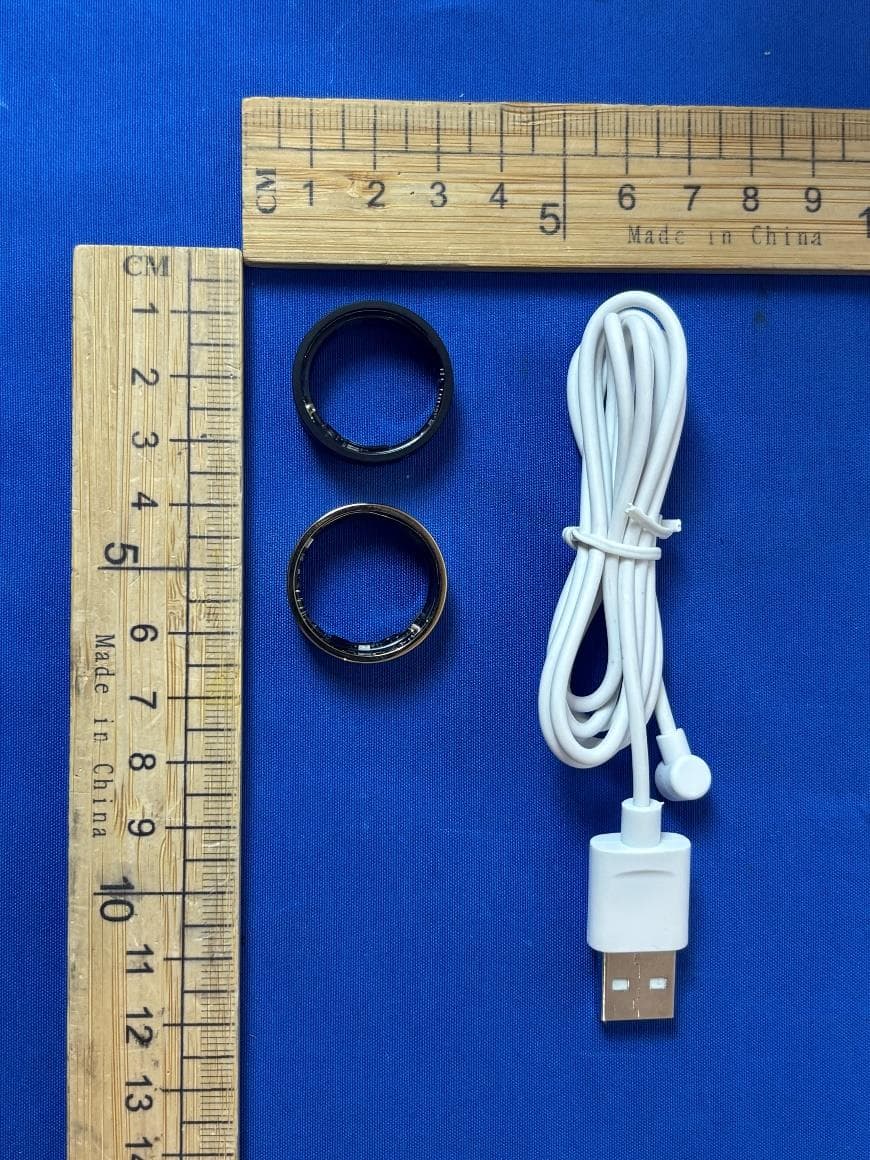
Click to zoom
Application Details
- Equipment Class
- DTS - Digital Transmission System
- Date of Grant
- Nov 28, 2025
- Application Purpose
- Original Equipment
- Equipment Note
- mOrring
- Frequency Range
- 2402.00000000 - 2480.00000000
- Country
- China
Documents & Files
Document Text
Text extracted from the exhibit documents filed with the FCC. Open a document above to read the original.
Users Manual
Smart Ring Instruction Manual Bluetooth version: V5.1 Battery (Max): 4.2V Operating frequency: 2400-2483.5MHz Transmitting power: 4dBm Control distance: <10 meters Endurance time: up to 48 hours Operating temperature: 15~40°C Model :TY-mOrr-R01 Manufacturer Name: Guangzhou Tyrafos Semiconductor Technology Co., Ltd Manufacturer address: Room 1101-1103, 11th Floor, Building C4, Guigu Science and Techno Guangzhou City Operation mode: 1. Scan the QR code to download the app 2. Register an account: First time using the app, and complete the personal information content according to the system prompts prompted by the system. 3. There are two ways to pair a mobile phone: ① Turn on the Bluetooth switch on your phone, and then open the mOrring Ring App, ②: Directly enter the mOrring Ring APP, and the APP prompts to turn on Bluetooth, Select "Click to bind" on the mobile app, choose the correct ring Bluetooth name to connect and bind. (Example: XXmOrr) 4.Wearing the ring: Put the mOrr ring on a suitable finger (recommended index finger/ middle finger/ring finger), adjust it to the appropriate wearing position, The laser engraving mOrr should be directed towards the middle of the finger pad, as shown in Figure 2. The physiological signal detection area (PD&CIS device) needs to be close to the finger pad position . Picture1 Picture 2 5. After the Bluetooth connection of the ring, enter the "Blood Pressure" interface, click " Start Calibration", and use a professional cuff or arm type blood pressure monitor, Modify the measured values, click the "Confirm" button for calibration, and display "Reset" after calibration is complete 6. Click the 'Manual Measurement or Measurement' button to start testing blood pressure, 7.Click on the "Measure" button on the heart rate and blood oxygen interface to measure heart rate and blood oxygen 8. Ring charging method FCC Statement 1.This device complies with Part 15 of the FCC Rules. Operation is subject to the following two conditions: (1)This device may not cause harmful interference. (2)This device must accept any interference received, including interference that may cause undesired operation. 2. Changes or modifications not expressly approved by the party responsible for compliance could void the user’s authority to operate the equipment. Note:This equipment has been tested and found to comply with the limits for a class B digital place flat The ring enters the warehouse, the red light of the ring flashes to charge, and the green light of the ring flashes to fully charge Ring storage+charging cable to charge the charging compartment, the red light inside the compartment lights up to charge the charging compartment, and the green light lights up to charge the ring Ring+charging cable for charging device,pursuant to Part 15 of the FCC Rules. These limits are designed to provide reasonable protection against harmful interference in a residential installation. This equipment generates uses and can radiate radio frequency energy and,if not installed and used in accordance with the instructions,may cause harmful interference to radio communications.However,there is no guarantee that interference will not occur in a particular installation.if this equipment does cause harmful interference to radio or television reception,which can be determined by turning the equipment off and on,the user is encouraged to try to correct the interference by one or more of the following measures: • Reorient or relocate the receiving antenna. • Increase the separation between the equipment and receiver. • Connect the equipment into an outlet on a circuit different from that to which the receiver is connected. • Consult the dealer or an experienced radio/TV technician for help. The device has been evaluated to meet general RF exposure requirement. The device can be used in portable exposure condition without restriction.
Attestation Statements
* theapplicantmustdesignateacontactlocatedintheUnitedStatesforpurposesofactingasthe applicant’sagentforserviceofprocess,regardlessofwhethertheapplicantisadomesticorforeign entity.AnapplicantlocatedintheUnitedStatesmaydesignateitselfastheagentforserviceofprocess. SC5105770 U.S.AgentDesignationforServiceofProcess- CertificationAttestationLetter 11/21/2025 TO:FederalCommunicationsCommission 7435OaklandMillsRoad Columbia,MD21046 ATTN.:ReviewingEngineer FCCID:2BSVG-MORR-R01 FRNofapplicant:0037624517 Persection2.911(d)(7)oftheFCCrules,[TYRAFOSINTERNATIONALCO.,LIMITED](“the applicant”)certifiesthattheequipmentforwhichauthorizationissoughtisdesignatedtothe followingU.S.agent*forserviceofprocess: CompanyName:GlobalProductServicesandConsultationLLC FCCRegistrationNumber(FRN):0033406703 PhysicalU.S.CompanyAddress:328WPalmAve.,Monrovia,CA91016,UnitedStates ContactPerson:MichaelChan Tel:+16263664358 AgentEmailAddress:[email protected] Theabovecontactpersonacceptstheobligationforserviceofprocess. Theapplicantacceptstomaintainanagentfornolessthanoneyearafterthegranteehas terminatedallmarketingandimportationortheconclusionofanyCommission-related proceedinginvolvingtheequipment. ApplicantSigned:AgentSigned(ifdifferentfromApplicant): Signed: Printedname:ChengChangLai Title:SeniorDirector CompanyName:TYRAFOSINTERNATIONAL CO.,LIMITED Address:Room1212,12/F.,505Hennessy Road,CausewayBay,HongKong Signed: Printedname:MichaelChan Title:TechnicalDirector CompanyName:GlobalProductServicesand ConsultationLLC Date:11/24/2025 Date:11/21/2025
Attestation Statements
TYRAFOS INTERNATIONAL CO.,LIMITED 2025-11-21 Eurofins Electrical and Electronic Testing NA, Inc. 914 West Patapsco Avenue Baltimore, MD 21230 RE: Attestation Statements Part 2.911(d)(5)(i) request for (FCC ID: 2BSVG-MORR-R01) [TYRAFOS INTERNATIONAL CO.,LIMITED] (“the applicant”) certifies that the equipment for which authorization is sought is not “covered” equipment prohibited from receiving an equipment authorization pursuant to section 2.903 of the FCC rules. We also certify that, as of the date of the filing of the application, the equipment does not utilize cyber-security or anti-virus software from Kaspersky Lab, Inc, or any of its successors and assignees, which is also on the “covered list”. Sincerely, Cheng Chang Lai Senior Director TYRAFOS INTERNATIONAL CO.,LIMITED Room 1212, 12/F., 505 Hennessy Road, Causeway Bay, Hong Kong TYRAFOS INTERNATIONAL CO.,LIMITED 2025-11-21 Eurofins Electrical and Electronic Testing NA, Inc. 914 West Patapsco Avenue Baltimore, MD 21230 RE: Attestation Statements Part 2.911(d)(5)(ii) request for (FCC ID: 2BSVG-MORR-R01) [TYRAFOS INTERNATIONAL CO.,LIMITED] (“the applicant”) certifies that, as of the date of the filing of the application, the applicant is not identified on the Covered List as an entity producing “covered” equipment. Sincerely, Cheng Chang Lai Senior Director TYRAFOS INTERNATIONAL CO.,LIMITED Room 1212, 12/F., 505 Hennessy Road, Causeway Bay, Hong Kong
External Photos
External Photographs View of EUT-1 View of EUT-2 Page 2 of 5 View of EUT-3 View of EUT-4 Page 3 of 5 View of EUT-5 View of EUT-6 Page 4 of 5 View of EUT-7 View of EUT-8 Page 5 of 5 View of EUT-9
ID Label/Location Info
Size: 3*10mm Material: PET FCC ID: 2BSVG-MORR-R01
Internal Photos
Internal Photographs Internal View of EUT-1 Internal View of EUT-2 Page 2 of 3 Internal View of EUT-3 Internal View of EUT-4 Page 3 of 3 Internal View of EUT-5 Antenna
RF Exposure Info
RF EXPOSURE EVALUATION EUT Specification FCC ID 2BSVG-MORR-R01 Antenna gain (Max) 2.28 dBi Operation Frequency 2402-2480MHz Classification Per Stipulated Test Standard §15.247(i), §2.1093 Modulation GFSK Max. output power 0.24 dBm(1.0568mW) Test Requirement: According to ß15.247(i) and ß1.1307(b)(1), systems operating under the provisions of this section shall be operated in a manner that ensures that the public is not exposed to radio frequency energy level in excess of the Commission’s guidelines. Routine SAR evaluation refers to that specifically required by ß2.1093, using measurements or computer simulation. When routine SAR evaluation is not required, portable transmitters with output power greater than the applicable low threshold require SAR evaluation to quality for TCB approval. One antenna is available for the EUT. The minimum separation distance is 5mm. Transmit Frequency (MHz) Mode Measured Power (dBm) Tune up Power (dBm) Max tune up power(dBm) Calculation Result 1-g SAR Verdict 2480 BLE 2Mbps 0.24 0±1 1 0.3965 3 PASS Note: No need for SAR test Signature: Shawn Wen Date: 2025-11-20
Test Report
承 認 書 SPECIFICATION FOR APPROVAL 客戶名稱 CUSTOMER : 客戶料號 CUSTOMER’S P/N : 料號 PART NUMBER : KH-1608-H08 規格 DESCRIPTION : Chip Antenna 1608 MH-Ant 2.45G Type H08 版本 VERSION : V1.0 日期 ISSUE DATE : 2021/03/03 客 戶 承 認 CUSTOMER APPROVED 工 程 部 R&D CENTER 承 認 APPROVAL 確 認 CHECKED 製 作 DRAWN 深圳市金航标电子有限公司 1/12 WWW.BDS666.COM 0755-83044319 赖积任 张松强 严专专 2/12 WWW.BDS666.COM 0755-83044319 1608 Chip antenna For Bluetooth / WLAN Applications Dimension (mm) L 1.70 ± 0.20 W 0.93 ± 0.20 T 0.75 ± 0.20 P/N: KH-1608-H08 3/12 WWW.BDS666.COM 0755-83044319 Part Number Information KH 1608 H 245 H 08 A B C D E F A Product Series Antenna B Dimension L x W 1.6X0.8mm (+-0.2mm) C Material High K material D Working Frequency 2.4 ~ 2.5GHz E Feeding mode Monopole & Single Feeding F Antenna type Type = 08 1. Electrical Specification Remark : Bandwidth & Peak Gain was measured under evaluation board of next page Specification Part Number KH-1608-H08 Central Frequency 2450 MHz Bandwidth 120 (Min.) MHz Return Loss -10(Max) dB Peak Gain 2.28 dBi Impedance 50 Ohm Operating Temperature -40~+110 °C Maximum Power 4 W Resistance to Soldering Heats 10 ( @ 260°C) sec. Polarization Linear Azimuth Beamwidth Omni-directional Termination Cu / Sn (Leadless) 4/12 WWW.BDS666.COM 0755-83044319 2. Recommended PCB Pattern 1. Evaluation Board Dimension (若淨空區夠大,建議在天線尾段加Trace,效能更佳) Unit : mm 2. Evaluation Board Dimension (若淨空區夠大,建議在天線尾段加Trace,效能更佳) 3. Evaluation Board Dimension 5/12 WWW.BDS666.COM 0755-83044319 Suggested Matching Circuit 重要資訊 : 匹配元件建議使用精準度高的電感±0.1~0.3nH、電容±0.1pF 1. Layout Dimensions in Clearance area(Size=5.5*4mm) 50 ohm transmission Line Matching Circuit 2. Layout Dimensions in Clearance area(Size=5.5*4mm) 50 ohm transmission Line Matching Circuit 1~10nH None 0Ω 1.5pF 6/12 WWW.BDS666.COM 0755-83044319 3. Layout Dimensions in Clearance area(Size=5*3mm) 50 ohm transmission Line Matching Circuit FootPrint (Unit : mm) 7/12 WWW.BDS666.COM 0755-83044319 3. Measurement Results Return Loss 8/12 WWW.BDS666.COM 0755-83044319 Radiation Pattern Efficiency Peak Gain Directivity 2400MHz 50.65 % 1.80 dBi 3.95 dBi 2450MHz 53.27 % 2.28 dBi 4.42 dBi 2500MHz 50.32 % 1.77 dBi 4.15 dBi Chamber Coordinate System Y Z X 9/12 WWW.BDS666.COM 0755-83044319 4.Reliability and Test Condictions ITEM REQUIREMENTS TEST CONDITION Solderability 1. Wetting shall exceed 90% coverage 2. No visible mechanical damage Pre-heating temperature:150°C/60sec. Solder temperature:230±5°C Duration:4±1sec. Solder:Sn-Ag3.0-Cu0.5 Flux for lead free: rosin Solder heat Resistance 1. No visible mechanical damage 2. Central Freq. change :within ± 6% 10 ± 0.5 sec. 60 sec . . T E M P ( °C ) 150 °C 2 6 0 °C Pre-heating temperature:150°C/60sec. Solder temperature:260±5°C Duration:10±0.5sec. Solder:Sn-Ag3.0-Cu0.5 Flux for lead free: rosin Component Adhesion (Push test) 1. No visible mechanical damage The device should be reflow soldered(230±5°C for 10sec.) to a tinned copper substrate A dynometer force gauge should be applied the side of the component. The device must with-ST-F 0.5 Kg without failure of the termination attached to component. Component Adhesion (Pull test) 1. No visible mechanical damage Insert 10cm wire into the remaining open eye bend ,the ends of even wire lengths upward and wind together. Terminal shall not be remarkably damaged. Thermal shock 1. No visible mechanical damage 2. Central Freq. change :within ±6% Phase Temperature(°C) Time(min) 1 +110±5°C 30±3 2 Room Temperature Within 3sec 3 -40±2°C 30±3 4 Room Temperature Within 3sec +110°C=>30±3min -40°C=>30±3min Test cycle:10 cycles The chip shall be stabilized at normal condition for 2~3 hours before measuring. Resistance to High Temperature 1. No visible mechanical damage 2. Central Freq. change :within ±6% 3. No disconnection or short circuit. Temperature: +110±5°C Duration: 1000±12hrs The chip shall be stabilized at normal condition for 2~3 hours before measuring. Resistance to Low Temperature 1. No visible mechanical damage 2. Central Freq. change :within ±6% 3. No disconnection or short circuit. Temperature:-40±5°C Duration: 1000±12hrs The chip shall be stabilized at normal condition for 2~3 hours before measuring. Humidity 1. No visible mechanical damage 2. Central Freq. change :within ±6% 3. No disconnection or short circuit. Temperature: 40±2°C Humidity: 90% to 95% RH Duration: 1000±12hrs The chip shall be stabilized at normal condition for 2~3 hours before measuring. 4±1 sec. 60sec TEMP (°C) 150°C 230°C 10/12 WWW.BDS666.COM 0755-83044319 5.Soldering and Mounting Mildly activated rosin fluxes are preferred. The minimum amount of solder can lead to damage from the stresses caused by the difference in coefficients of expansion between solder, chip and substrate. The terminations are suitable for all wave and re-flow soldering systems. If hand soldering cannot be avoided, the preferred technique is the utilization of hot air soldering tools. Recommended temperature profiles for re-flow soldering in Figure 1. Products attachment with a soldering iron is discouraged due to the inherent process control limitations. In the event that a soldering iron must be employed the following precautions are recommended. ‧Preheat circuit and products to 150°C ‧Never contact the ceramic with the iron tip ‧Use a 20 watt soldering iron with tip diameter of 1.0mm ‧280°C tip temperature (max) ‧1.0mm tip diameter (max) ‧Limit soldering time to 3 sec. SOLDERING COOLING NATURAL PRE-HEATING TEMPERATURE(°C) 60~120 s 10s max. 30~60s 250~260 230 180 150 TIME(sec.) Reflow Soldering SOLDERING COOLING NATURAL PRE-HEATING TEMPERATURE(°C) within 3s Gradual cooling 150 TIME(sec.) Iron Soldering Over 60s 350 300 11/12 WWW.BDS666.COM 0755-83044319 6.Packaging Information ◆ Tape Specification: W Ao Bo Ko P F E D D1 Po P2 t 8.0 ±0.30 1.10± 0.05 1.90 ±0.10 1.10± 0.10 4.00 ±0.05 3.50 ±0.05 1.75 ±0.10 1.50 ±0.10 0.00 ±0.10 4.00 ±0.10 2.00 ±0.05 0.23 ±0.05 ◆ Reel Specification: (7’’, Φ180 mm) Tape Width(mm) A(mm) B(mm) C(mm) D(mm) Chip/Reel(pcs) 8 9.0±0.5 6…
Text truncated - open the document above for the full version.
Test Report
TRF No.: 04-E001-0B TRF Originator: GTG TRF Date: 2023-12-13 Web: www.gtggroup.com E-mail: [email protected] Tel.: 86-400 755 8988 CFR 47 FCC PART 15 SUBPART C(DTS) TEST REPORT For mOrring MODEL NUMBER: TY–mOrr-R01 REPORT NUMBER: E04A25110160F00501 ISSUE DATE: November 20, 2025 FCC ID: 2BSVG-MORR-R01 Prepared for TYRAFOS INTERNATIONAL CO.,LIMITED Room 1212, 12/F., 505 Hennessy Road, Causeway Bay, Hong Kong Prepared by Guangdong Global Testing Technology Co., Ltd. Room 101-105, 203-210, Building 1, No.2, Keji 8 Road, Songshan Lake Park, Dongguan city, Guangdong, People’s Republic of China, 523808 This report is based on a single evaluation of the submitted sample(s) of the above mentioned product, it does not imply an assessment of the production of the products. This report shall not be reproduced, except in full, without the written approval of Guangdong Global Testing Technology Co., Ltd. REPORT NO.: E04A25110160F00501 Page 2 of 74 TRF No.: 04-E001-0B Global Testing , Great Quality. Revision History Rev. Issue Date Revisions Revised By V0 November 20, 2025 Initial Issue REPORT NO.: E04A25110160F00501 Page 3 of 74 TRF No.: 04-E001-0B Global Testing , Great Quality. Summary of Test Results Test Item Clause Limit/Requirement Result Antenna Requirement ANSI C63.10-2020 FCC Part 15.203/15.247 (c) Pass AC Power Line Conducted Emission ANSI C63.10-2020 FCC Part 15.207 Pass Conducted Output Power ANSI C63.10-2020 FCC Part 15.247 (b)(3) Pass 6dB Bandwidth and 99% Occupied Bandwidth ANSI C63.10-2020 FCC Part 15.247 (a)(2) Pass Power Spectral Density ANSI C63.10-2020 FCC Part 15.247 (e) Pass Conducted Band edge and spurious emission ANSI C63.10-2020 FCC Part 15.247(d) Pass Radiated Band edge and Spurious Emission ANSI C63.10-2020 FCC Part 15.205/15.209 Pass Duty Cycle ANSI C63.10-2020 None; for reporting purposes only. Pass *This test report is only published to and used by the applicant, and it is not for evidence purpose in China. *The measurement result for the sample received is <Pass> according to <CFR 47 FCC PART 15 SUBPART C(DTS)> when <Accuracy Method> decision rule is applied. REPORT NO.: E04A25110160F00501 Page 4 of 74 TRF No.: 04-E001-0B Global Testing , Great Quality. CONTENTS 1. ATTESTATION OF TEST RESULTS ..................................................................................... 5 2. TEST METHODOLOGY ......................................................................................................... 6 3. FACILITIES AND ACCREDITATION ..................................................................................... 6 4. CALIBRATION AND UNCERTAINTY ................................................................................... 7 4.1. MEASURING INSTRUMENT CALIBRATION ........................................................... 7 4.2. MEASUREMENT UNCERTAINTY ............................................................................ 7 5. EQUIPMENT UNDER TEST .................................................................................................. 8 5.1. DESCRIPTION OF EUT ........................................................................................... 8 5.2. CHANNEL LIST ........................................................................................................ 8 5.3. MAXIMUM CONDUCTED OUTPUT POWER ........................................................... 9 5.4. TEST CHANNEL CONFIGURATION ........................................................................ 9 5.5. THE WORSE CASE POWER SETTING PARAMETER ............................................ 9 5.6. DESCRIPTION OF AVAILABLE ANTENNAS ........................................................... 9 5.7. EUT ACCESSORY ................................................................................................. 10 5.8. SUPPORT UNITS FOR SYSTEM TEST ................................................................. 10 5.9. SETUP DIAGRAM .................................................................................................. 10 6. MEASURING EQUIPMENT AND SOFTWARE USED......................................................... 12 7. ANTENNA PORT TEST RESULTS ..................................................................................... 14 7.1. Conducted Output Power ........................................................................................ 14 7.2. 6dB Bandwidth and 99% Occupied Bandwidth ....................................................... 15 7.3. Power Spectral Density ........................................................................................... 17 7.4. Conducted Band edge and spurious emission ........................................................ 18 7.5. Duty Cycle .............................................................................................................. 20 8. RADIATED TEST RESULTS ............................................................................................... 21 8.1. Radiated Band edge and Spurious Emission .......................................................... 27 9. ANTENNA REQUIREMENT ................................................................................................ 39 10. AC POWER LINE CONDUCTED EMISSION ......................................................... 40 11. TEST DATA - Appendix A ..................................................................................... 43 REPORT NO.: E04A25110160F00501 Page 5 of 74 TRF No.: 04-E001-0B Global Testing , Great Quality. 1. ATTESTATION OF TEST RESULTS Applicant Information Company Name: TYRAFOS INTERNATIONAL CO.,LIMITED Address: Room 1212, 12/F., 505 Hennessy Road, Causeway Bay, Hong Kong Manufacturer Information Company Name: Guangzhou Tyrafos Semiconductor Technologies Co., Ltd. Address: 1101-1103, 11th Floor, Building C4, Guigu Science and Technology Park, No. 262 Kefeng Road, Huangpu District, Guangzhou City EUT Information Product Description: mOrring Model: TY–mOrr-R01 Series Model: / Brand: mOrr Sample Received Dat…
Text truncated - open the document above for the full version.
Test Setup Photos
Setup Photographs AC Power Line Conducted Emission Page 2 of 3 Radiated Band edge and Spurious Emission Page 3 of 3
Contact Information
Applicant
Cheng Chang Lai(Senior Director)
[email protected]Fax: /
Test Firm
Guangdong Global Testing Technology Co., Ltd.Shawn Wen
Technical Specifications
| # | Rule Parts | Frequency Range | Power Output |
|---|---|---|---|
| 1 | 15C | 2.40 GHz - 2.48 GHz | 1.10 mW |