2BUYX-G680Dash Cam
Shenzhen Qianli Antong Technology Co., Ltd.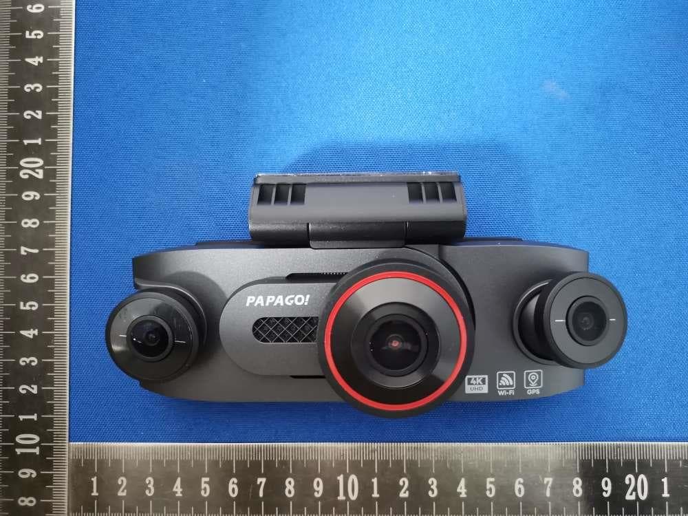
Click to zoom
Application Details
- Equipment Class
- DTS - Digital Transmission System
- Date of Grant
- Mar 12, 2026
- Application Purpose
- Original Equipment
- Equipment Note
- Dash Cam
- Frequency Range
- 2412.00000000 - 2462.00000000
- Country
- China
Documents & Files
Document Text
Text extracted from the exhibit documents filed with the FCC. Open a document above to read the original.
Users Manual
Thank you Quick Start Guide NO 1 PRODUCT BASIC INTRODUCTION Cautions Product Components Component Guide If you have any questions, need technical support, please don't hesitate to contact us. Our dedicated customer care team is always here for you and will respond within 24 hours. [email protected] In the Box Dash Camera Cleaning Cloth Adhesive Cable Clip×4 Easy Pry Tool Static Stickerx4 Rear Camera Adhesive Pads (2on Cameras) Car Charger User Manual To prevent personal injury or equipment damage, please read and follow the below safety guidelines carefully: Be sure to read and understand the product manual before use, and keep it properly for future reference. Use only genuine accessories provided by the manufacturer. The company shall not be liable for any damage caused by non-genuine accessories from other manufacturers. Do not disassemble, modify or repair the product by yourself; any damage to the main unit resulting from such actions is not covered by the warranty. Do not install the product in high-humidity areas, areas exposed to direct sunlight or extreme high temperatures, environments with ammable and explosive gases or liquids, or any areas that block the driver's line of sight or compromise driving safety. In case of abnormal conditions, stop using the product immediately, disconnect the power supply and contact customer service. Drive safely! Never operate the app or the device while driving to avoid tra c accidents caused by distraction. Ensure the vehicle is parked in a safe area before any operation. Conduct a power-on test before installation, and remove the protective lms from the display screen and lens before use. Be sure to format the memory card on the main unit before its rst use to ensure stable reading and writing performance of the card. The vehicle must only be driven after the product is securely installed. Safety Precautions 01 1 2 3 4 5 6 7 8 9 Component Guide 02 button Left Camera GPS Mount Rear Camera Port Type-C Port Right Camera Screen Memory Card SlotSpeakerFront Camera Reset Button Menu Button Up Button Power Button Down Button OK Button 1 2 3 4 5 Button Functions 03 Menu Button Press Once - to enter/exit settings menu. Press Once - to go back to the previous screen. (in menu mode) Up Button Press Once (Recording Interface) - take photo. Press Once (Menu Interface) - move up one line . Press Once (Playback Interface) - previous video. Hold 3s - lock/unlock video. (while recording, indicator turns yellow when locked) Press Once - turn screen o /on. (while device is on) Hold 3s - power o /on. (while device is on) Power Button Down Button Press Once (Recording Interface) - switch front / rear camera, spit screen mode. Press Once (Menu Interface) - move down one line. Press Once (Playback Interface) - play next video. Hold 3s - turn Wi-Fi on/o . (in recording mode) OK Button Press Once - Pause/Stop Recording. Press Once - con rm/select. (menu mode) Hold 3s - Microphone on/o . (in recording mode) 1 2 3 4 5 FCC War ning This device complies w it h Par t 15 of t he FCC Rules. Oper at ion is subject t o t he f ollow ing t w o condit ions: (1) This device may not cause har mf ul int er f er ence, and (2 ) t his device must accept any int er f er ence received, including int er f er ence t hat may cause undesir ed oper at ion. NOTE 1: This equipment has been t est ed and f ound t o comply w it h t he limit s f or a Class B digit al device, pur suant t o par t 15 of t he FCC Rules. These limit s ar e designed t o pr ovide r easonable pr ot ect ion against har mf ul int er f er ence in a r esident ial inst allat ion. This equipment gener at es, uses and can r adiat e r adio f r equency ener gy and, if not inst alled and used in accor dance w it h t he inst r uct ions, may cause har mf ul int er f er ence t o r adio communicat ions. How ever , t her e is no guar ant ee that int er f er ence w ill not occur in a par t icular inst allat ion. If t his equipment does cause har mf ul int er f er ence t o r adio or t elevision r ecept ion, w hich can be det er mined by t ur ning t he equipment of f and on, t he user is encour aged t o t r y t o cor r ect t he int er f er ence by one or mor e of t he f ollow ing measur es: - Reor ient or r elocat e t he r eceiving ant enna. - Incr ease t he separ at ion bet w een t he equipment and r eceiver . -Connect t he equipment int o an out let on a cir cuit dif f er ent f r om t hat t o w hich t he r eceiver is connect ed. -Consult t he dealer or an exper ienced r adio/ TV t echnician f or help. NOTE 2 : Any changes or modif icat ions t o t his unit not expr essly appr oved by t he par t y r esponsible f or compliance could void t he user 's aut hor it y t o oper at e t he equipment . RF Exposur e St at ement To maint ain compliance w it h FCC'S RF Exposur e guidelines, This equipment should be inst alled and oper at ed w it h minimum 2 0 cm bet w een t he r adiat or and your body. This device and it s ant enna(s) must not be co-locat ed or oper at ion in conjunct ion w it h any ot her ant enna or t r ansmit t er .
Attestation Statements
Shenzhen Qianli Antong Technology Co., Ltd. U.S. Agent Letter of Attestation To: Federal Communications Commission 7435 Oakland Mills Road, Columbia, MD 21046, USA Date: March 11, 2026 Ref: Attestation Statement – Part 2.911(d)(7) filing FCC ID: 2BUYX-G680 Shenzhen Qianli Antong Technology Co., Ltd. (“the applicant”) certifies that, as of the date of the filing of the application, CLF Import and Export Limited (“the agent”) is our designated U.S. agent for service of process for the above reference FCC ID. The applicant accepts to maintain an agent for service of process in the United States for no less than one year after either the grantee has permanently terminated all marketing and importation of the applicable equipment within the U.S., or the conclusion of any Commission-related administrative or judicial proceeding involving the equipment, whichever is later. The applicant further acknowledges it is our responsibility to inform the FCC whenever the agent information changes. CLF Import and Export Limited ("the agent) understand it is the agent's obligation to accept service of process in the United States for matters related to the applicable equipment, and at the physical U.S. address and email address. Designated U.S. Agent Company Name: CLF Import and Export Limited FRN: 0033489683 Address: 1312 17th Street #692, Denver, CO 80202, United States Signature: Contact Person: David Chen Tel: +1 949 254 2565 Email: [email protected] Applicant Company Name: Shenzhen Qianli Antong Technology Co., Ltd. FRN: 0038090908 Address: Room 302, Building A, No. 47-2, Fuqian Road, Fumin Community, Fucheng Subdistrict, Longhua District, Shenzhen, China Signature: Contact Person: Li Xu Tel: +86-18123680172 Email: [email protected]
Attestation Statements
Rev 1/26/2023 Shenzhen Qianli Antong Technology Co., Ltd. Federal Communications Commission Authorization and Evaluation Division 7435 Oakland Mills Road Columbia, MD 21046 USA Date: 03-11-2026 Ref: Attestation Statements Part 2.911(d)(5)(i) Filing FCC ID: 2BUYX-G680 [Shenzhen Qianli Antong Technology Co., Ltd.] certifies that the equipment for which authorization is sought is not “covered” equipment prohibited from receiving an equipment authorization pursuant to section 2.903 of the FCC rules. [Shenzhen Qianli Antong Technology Co., Ltd.] certifies that the equipment for which authorization is sought does not include cybersecurity or anti-virus software produced or provided by Kaspersky Lab, Inc. or any of its successors and assignees, including equipment with integrated Kaspersky Lab, Inc. (or any of its successors and assignees) cybersecurity or anti-virus software pursuant to DA-24-886 and KDB 986446 D01 Covered Equipment Guidance section B(2a). Device is inherently compliant based on hardware limitations or software controls. or A Software Bill of Materials (SBOM) is provided to the TCB for review, and The end-user or third parties cannot install additional software on this device. Sincerely, (Applicant signature) (Applicant printed name) Li Xu Rev 1/26/2023 Shenzhen Qianli Antong Technology Co., Ltd. Federal Communications Commission Authorization and Evaluation Division 7435 Oakland Mills Road Columbia, MD 21046 USA Date: 03-11-2026 Ref: Attestation Statements Part 2.911(d)(5)(ii) Filing FCC ID: 2BUYX-G680 [Shenzhen Qianli Antong Technology Co., Ltd.] ce8rtifies that, as of the date of the filing of the application, the applicant is not identified on the Covered List (as a specifically named entity or any of its subsidiaries or affiliates) as an entity producing “covered” equipment. Sincerely, (Applicant signature) (Applicant printed name) Li Xu
Cover Letter(s)
Shenzhen Qianli Antong Technology Co., Ltd. Date: March 11, 2026 Product Model Number: G680 FCC ID: 2BUYX-G680 To whom it may concern, Re: Product Certification Representative Authorization Letter We authorize QAI Laboratories Ltd. 3980 North Fraser Way, Burnaby B.C. Canada V5J 5K5 to act on our behalf on all matters concerning the above named equipment. This shall include the following: • Testing • Approval applications and procedures We declare that QAI Laboratories Ltd. is allowed to forward all information related to the approval project to the applied certification body and to the notification entities and to discuss any issues concerning the approval application. Any and all acts carried out by QAI Laboratories Ltd. on our behalf shall have the same effect as acts of our own. By: Li Xu Contact Listed on FCC Wesbite Title: Manager Email: [email protected] Telephone: +86-18123680172 On behalf of: Shenzhen Qianli Antong Technology Co., Ltd.
Cover Letter(s)
Shenzhen Qianli Antong Technology Co., Ltd. Office of Engineering Technology Federal Communications Commission 7435 Oakland Mills Road Columbia, MD 21046 USA Date: March 11, 2026 Subject; Request for Confidentiality FCC ID: 2BUYX-G680 To Whom It May Concern, Pursuant to the provisions of the Commission’s rules Title 47 Sections §0.457 and §0.459, we are requesting the Commission to withhold the following attachment(s) as confidential documents from public disclosure indefinitely. These documents contain detailed system and equipment descriptions and are considered as proprietary information in operation of the equipment. The public disclosure of these documents might be harmful to our company and would give competitors an unfair advantage in the market. Schematic Diagram Block Diagram Parts List Operational Description Tune-up Procedure Software Security Requirements for UNII devices It is our understanding that all measurement test reports, FCC ID label format and correspondence during the certification review process cannot be granted as confidential documents and this information will be available for public review once the grant of equipment authorization is issued. Sincerely, Signature: Name: Li Xu Title: Manager
External Photos
Report No: SSP26020109-1E FCC ID: 2BUYX-G680 Annex of Test Report Annex A. EUT External Photos Model: G680 EUT View 1 EUT View 2 Report No: SSP26020109-1E FCC ID: 2BUYX-G680 Annex of Test Report EUT View 3 EUT View 4 Report No: SSP26020109-1E FCC ID: 2BUYX-G680 Annex of Test Report EUT View 5 EUT View 6 Report No: SSP26020109-1E FCC ID: 2BUYX-G680 Annex of Test Report EUT View 7
ID Label/Location Info
Report No: SSP26020109-1E FCC ID: 2BUYX-G680 Annex of Test Report Annex D. Label and Information FCC Label Sample Label Size: 1.3cm * 0.5cm FCC Label Specifications Text is Black in color and is justified. Labels are printed in indelible ink on permanent adhesive backing or silk-screened onto the EUT or shall be affixed at a conspicuous location on the EUT. Where the EUT is constructed in two or more sections connected by wires and marketed together, the above statement is required to be affixed only to the main control unit. When the EUT is so small or for such use that it is not practicable to place the statement on it, the above information shall be placed in a prominent location in the instruction manual or pamphlet supplied to the user or, alternatively, shall be placed on the container in which the device is marketed. FCC Label Location
Internal Photos
Report No: SSP26020109-1E FCC ID: 2BUYX-G680 Annex of Test Report Annex B. EUT Internal Photos Model: G680 EUT Internal View 1 EUT Internal View 2 SMD Antenna Report No: SSP26020109-1E FCC ID: 2BUYX-G680 Annex of Test Report EUT Internal View 3 EUT Internal View 4 Report No: SSP26020109-1E FCC ID: 2BUYX-G680 Annex of Test Report EUT Internal View 5 EUT Internal View 6 Report No: SSP26020109-1E FCC ID: 2BUYX-G680 Annex of Test Report EUT Internal View 7 EUT Internal View 8 Report No: SSP26020109-1E FCC ID: 2BUYX-G680 Annex of Test Report EUT Internal View 9 EUT Internal View 10 Report No: SSP26020109-1E FCC ID: 2BUYX-G680 Annex of Test Report EUT Internal View 11 EUT Internal View 12 Report No: SSP26020109-1E FCC ID: 2BUYX-G680 Annex of Test Report EUT Internal View 13 EUT Internal View 14 Report No: SSP26020109-1E FCC ID: 2BUYX-G680 Annex of Test Report EUT Internal View 15 EUT Internal View 16 GPS
RF Exposure Info
FCC ID: 2BUYX-G680 RF Exposure Evaluation Limits The criteria listed in the following table shall be used to evaluate the environment impact of human exposure to radio frequency (RF) radiation as specified in 1.1307(b) Limits for Maximum Permissible Exposure (MPE) Frequency range (MHz) Electric field strength (V/m) Magnetic field strength (A/m) Power density (mW/cm2) Averaging time (minutes) (A) Limits for Occupational/Controlled Exposures 0.3–3.0 614 1.63 *(100) 6 3.0–30 1842/f 4.89/f *(900/f2) 6 30–300 61.4 0.163 1.0 6 300–1500 f/300 6 1500–100,000 5 6 (B) Limits for General Population/Uncontrolled Exposure 0.3–1.34 614 1.63 *(100) 30 1.34–30 824/f 2.19/f *(180/f2) 30 30–300 27.5 0.073 0.2 30 300–1500 f/1500 30 1500–100,000 1.0 30 f = frequency in MHz Friis transmission formula: Pd = (Pout*G)/(4*pi*r2) Where Pd = power density in mW/cm2, Pout = output power to antenna in mW; G = gain of antenna in linear scale, Pi = 3.1416; R = distance between observation point and center of the radiator in cm Pd id the limit of MPE, 1 mW/cm2. If we know the maximum gain of the antenna and the total power input to the antenna, through the calculation, we will know the distance r where the MPE limit is reached. Test Procedure Software provided by client enabled the EUT to transmit and receive data at lowest, middle and highest channel individually. Test Result of RF Exposure Evaluation 2.4G Wi-Fi Mode Output power to antenna (dBm) Output power to antenna (mW) Power Density at R=20cm (mW/cm 2 ) Limit (mW/cm 2 ) Result 802.11b 14.03 25.29 0.0113 1.0 PASS So a SAR test is not required
Test Report
Report No: SSP26020109-1E FCC Test Report Page 1 of 48 FCC TEST REPORT FCC ID: 2BUYX-G680 Report No. : SSP26020109-1E Applicant : Shenzhen Qianli Antong Technology Co., Ltd. Product Name : Dash Cam Model Name : G680 Test Standard : FCC Part 15.247 Date of Issue : 2026-02-28 Shenzhen CCUT Quality Technology Co., Ltd. 1F, Building 35, Changxing Technology Industrial Park, Yutang Street, Guangming District, Shenzhen, Guangdong, China; (Tel.:+86-755-23406590 website: www.ccuttest.com) This test report is limited to the above client company and the product model only. It may not be duplicated without prior permitted by Shenzhen CCUT Quality Technology Co., Ltd. Report No: SSP26020109-1E FCC Test Report Page 2 of 48 Test Report Basic Information Applicant..................................: Shenzhen Qianli Antong Technology Co., Ltd. Address of Applicant...............: Room 302, Building A, No. 47-2, Fuqian Road, Fumin Community, Fucheng Subdistrict, Longhua District, Shenzhen, China Manufacturer..........................: Shenzhen Huanxiang Electronic Co,Ltd Address of Manufacturer........: Factory Building 8, Zone 1, Fuqiao Industrial Zone, Qiaotou Community, Fuhai Street, Bao'an District, Shenzhen City. 3rd floor of Factory Building 8 Product Name.........................: Dash Cam Brand Name.............................: PAPAGO! Main Model..............................: G680 Series Models..........................: - Test Standard..........................: FCC Part 15 Subpart C KDB 558074 D01 15.247 Meas Guidance v05r02 ANSI C63.4-2014 ANSI C63.10-2020 Date of Test .............................: 2026-02-05 to 2026-02-10 Test Result...............................: PASS Tested By ................................: (Coke Huang) Reviewed By............................: (Lorzix Luo) Authorized Signatory............: (Lahm Peng) Note : This test report is limited to the above client company and the product model only. It may not be duplicated without prior permitted by Shenzhen CCUT Quality Technology Co., Ltd.. All test data presented in this test report is only applicable to presented test sample. Report No: SSP26020109-1E FCC Test Report Page 3 of 48 CONTENTS 1. General Information ....................................................................................................................................................5 1.1 Product Information .............................................................................................................................................5 1.2 Test Setup Information..........................................................................................................................................6 1.3 Compliance Standards ...........................................................................................................................................7 1.4 Test Facilities ........................................................................................................................................................7 1.5 List of Measurement Instruments ..........................................................................................................................8 1.6 Measurement Uncertainty .....................................................................................................................................9 2. Summary of Test Results ........................................................................................................................................... 10 3. Antenna Requirement ............................................................................................................................................... 11 3.1 Standard and Limit.............................................................................................................................................. 11 3.2 Test Result .......................................................................................................................................................... 11 4. Conducted Emissions ................................................................................................................................................ 12 4.1 Standard and Limit.............................................................................................................................................. 12 4.2 Test Procedure.................................................................................................................................................... 12 4.3 Test Data and Results .......................................................................................................................................... 13 5. Radiated Emissions ................................................................................................................................................... 14 5.1 Standard and Limit.............................................................................................................................................. 14 5.2 Test Procedure.................................................................................................................................................... 14 5.3 Test Data and Results .......................................................................................................................................... 16 6. Band-edge Emissions(Radiated) ............................................................................................................................... 20 6.1 Standard and Limit.............................................................................................................................................. 20 6.2 Test Procedure.................................................................................................................................................... 20 6.3 Test Data and Results ........................................................................…
Text truncated - open the document above for the full version.
Test Report
1 /6 2.4GHz 5 221 SMD Antenna: RANT5221F245M02 1. Applicati ons WLAN , 80 2.11 b/g, Bl uetoot h , WLAN , etc ... 2. F eatu r es S MD , hi g h r e li ab ili ty, u l t r a Im pact , O mni- d ir ect i o n a l... 3. Pa rt Number Info rmati on RANT5221F245M02 (A)(B)(C) (D)(E)(F) (A)Produc t Ty p eSMD An t enna (B) Size Code 5 .1x2.0mm (±0 .2mm ) (C) MaterialHigh K material (D) Fr equency2.4 ~ 2.5GHz (E) Fe eding modePIFA & S ingl e F eed ing (F) Antenna typeTy pe=02 咏成國際科技有限公司 RAIN International Te chnology Co., Ltd. Room707,BuildingF,TonganZhichuangyuan,xixiangstreet, BaoanDistrict,Shenzhen. 2 /6 4. 00 2.3000 4. Product size 5020SMD antenna 5.ElectricalSpecification Specification Part Number RANT5221 F245M0 2 CentralFrequency 2450 MHz Bandwidth120 (Min.) MHz ReturnLoss -10 (Max) dB PeakGain 3.5 dBi Impedance 50Ohm OperatingTemperature - 40~+85 °C MaximumPower4W Resistanceto SolderingHeats 10 ( @ 260°C) sec. PolarizationLinear AzimuthBeamwidth Omni-directional TerminationSn (Leadless) 6. PCB FootPrint(Unit: mm) W Figure SymbolDimension(mm) L W A L (Long) 5. 10 ± 0.20 W (Wide) 2.00 ± 0.30 T( Thickness) 1.0 ± 0.30 A (Electrode width) 0.50 ± 0.20 4.0 3 /6 RecommendedPCBPattern EvaluationBoardDimension LayoutDimensionsinClearancearea (Size=7.0*5.0mm) 50ohmtransmissionLine MatchingCircuit 4 /6 0 0[dBd] 7.MeasurementResults ReturnLoss 7.2RadiationPattern +X 90 270 5 /6 260 °C 20-40s 217°C 150-200°C Pre-heating 60-150s 60-180s Time(s) 8.ReliabilityandTestCondictions Testitem Testcondition/Testmethod Specification Solderability JISC0050-4.6 JESD22-B102D *Solderbathtemperature:2355C *Immersiontime:20.5sec Solder:Sn3Ag0.5Cuforlead-free Atleast95%ofasurfaceofeachterminal electrodemustbecoveredbyfreshsolder. Leaching (Resistanceto dissolutionof metallization) IEC60068-2-58 *Solderbathtemperature:2605C *Leachingimmersiontime:30 0.5sec Solder:SN63A Lossofmetallizationontheedgesofeach electrodeshallnotexceed25%. Bendingtest JISC0051-7.4.1 Themiddlepartofsubstrateshallbe pressurizedbymeansofthepressurizingrod atarateofabout1mm/sperseconduntilthe deflectionbecomes1mm/sandthenpressure shallbemaintainedfor51sec. Measurementtobemadeafterkeepingat roomtemperaturefor242hours Nomechanicaldamage. Electricalspecificationshallsatisfythe descriptionsinelectricalcharacteristicsunder theoperationaltemperaturerangewithin-40 ~85°C. Resistancetosoldering heat JISC0050-5.4 *Preheatingtemperature:120~150 °C , 1minute. *Soldertemperature:2705C *Immersiontime:101sec Solder:Sn3Ag0.5Cuforlead-free Measurementtobemadeafterkeepingat roomtemperaturefor242hrs Nomechanicaldamage. Electricalspecificationshallsatisfythe descriptionsinelectricalcharacteristicsunder theoperationaltemperaturerangewithin-40 ~85°C. Lossofmetallizationontheedgesofeach electrodeshallnotexceed25%. 9.SolderingandMounting T e m p e r a t u r e ( ° C ) 6 /6 10. Antenna Application Guidelines If space permits, it is advisable not to choose antennas with too small a size. It is best for the antenna to have a large clearance from nearby objects; otherwise, the matching adjustment will become difficult and the radiation pattern will be severely distorted. There should be no circuit layout or grounding layer below the antenna. The antenna should not be placed too close to metal objects, such as batteries and chips, and it should not overlap with metal items like batteries. Be sure to keep the internal cables (such as the battery power cord) as far away from the antenna as possible. A monopole antenna requires a proper ground connection to achieve the best performance. Matching the antennas in the final product design can shorten the adjustment period; however, on the optical boards, adjustments often need to be made repeatedly. If the antennas are not properly matched, placing the same antennas on completely different layout boards may result in malfunction. Do not cover the antenna with a metal casing or a plastic casing containing metal. Do not use very thin antenna feed wires. The feed wire should have a certain width and should not be less than 0.1mm. Calculate the feedline impedance based on the thickness and dielectric constant of the PCB. A 50-ohm impedance will make it easier to adjust the antenna. The assembly of the chip antenna should be kept as far away as possible from the battery, EMI protection materials, foldable speakers, metal screws, LCD screens, etc. 11.Storageand TransportationInformation StorageConditions To maintainthe solderabilityof terminalelectrodes: 1.Temperatureand humidityconditions:-10~ 40 °C and 30~70%RH. 2.Recommendedproductsshouldbe usedwithin6 monthsfrom the time of delivery. 3.The packagingmaterialshouldbe kept whereno chlorineor sulfurexists in the air. TransportationConditions 1.Productsshouldbe handledwith care to avoiddamageor contamination from perspirationand skin oils. 2.The use of tweezersor vacuumpick up is stronglyrecommendedfor individualcomponents. 3.Bulk handlingshouldensurethat abrasionand mechanicalshockare minimized. 7 /6 FeatureSpecificationsTolerances W12.00±0.30 P4.00±0.10 E1.75±0.10 F 5.50±0.10 P2 2.00±0.10 D 1.50 +0.10 -0.00 Po4.00±0.10 10Po40.00±0.20 12.Packing (1)Quantity/Reel:2000pcs/Reel (2)Plastictape: a.TapeDrawingb.TapeDimensions(unit:mm)
Test Setup Photos
Report No: SSP26020109-1E FCC ID: 2BUYX-G680 Annex of Test Report Annex C. Test Photos Radiated Emission Test View Below 1GHz Radiated Emission Test View Above 1GHz
Contact Information
Applicant
Li Xu
[email protected]Fax: +86-18123680172
Technical Contact
Test Firm
Shenzhen CCUT Quality Technology Co., Ltd.Lahm Peng
Technical Specifications
| # | Rule Parts | Frequency Range | Power Output |
|---|---|---|---|
| 1 | 15C | 2.41 GHz - 2.46 GHz | 25.30 mW |