2BV2N-TNW-24000Nuwa Pen
Nuwa Labs, Inc.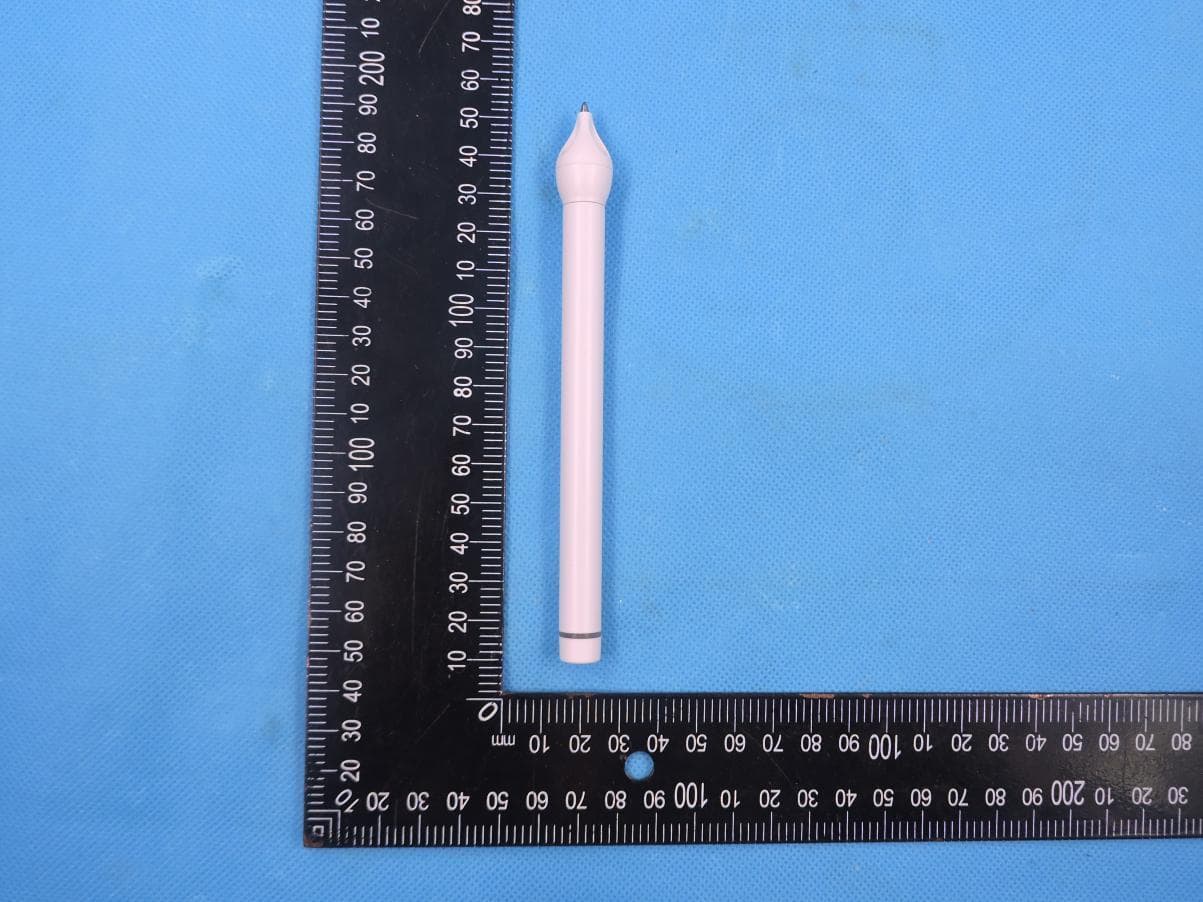
Click to zoom
Application Details
- Equipment Class
- DTS - Digital Transmission System
- Date of Grant
- Jul 14, 2026
- Application Purpose
- Original Equipment
- Equipment Note
- Nuwa Pen
- Frequency Range
- 2402.00000000 - 2480.00000000
- Company
- Nuwa Labs, Inc.
- Country
- United States
Documents & Files
Document Text
Text extracted from the exhibit documents filed with the FCC. Open a document above to read the original.
Users Manual
nuwapen.com 2. BEFORE USING NUWA PEN Connect the Case with the Nuwa Pen inside via the USB-C cable until fully charged (refer to image A). While charging, the LEDs on the case slowly pulse with a white light. Once fully charged, the light will turn solid white. (See image B). Support your pen by calibrating it via the app; follow the instructions here: www.nuwapen.com/calibrate -nuwapen. 8. NUWA SUPPORT 9. REQUEST THIS GUIDE IN YOUR LANGUAGE For support, information, and the latest software downloads, visit www.nuwapen.com or contact our customer service at [email protected]. 7. PROPER USE OF NUWA PEN For guidance on how to properly use Nuwa Pen, please refer to the Safety Instructions attached with your product and the User Manual found on the Nuwa website at www.nuwapen.com/user- manual. We value your understanding. Nuwa is happy to provide you with a physical copy of this guide in your native language free of charge. Please contact [email protected] to make the request. Do not use a different charging cable other than the one attached! 1. TECHNICAL DETAILS 1. Cartridge 2. Cameras 3. Charging points 4. LED Light 5. LED Light front - indicates charges on the inside 6. LED Light side - indicates case charging status 7. Reset pinhole A 321 3. HOW TO PAIR YOUR NUWA PEN WITH YOUR SMARTPHONE Your Nuwa Pen works with Android and iOS devices. Download and open Nuwa App from the Apple Store™ or Google Play™ Store. You are ready to launch the Nuwa App! For more information on how to manage the account registration setting, language transcription and features, settings, login, and subscriptions, Nuwa Pen App status information, troubleshooting, pairing and more. Please check out the Nuwa App section on our website: www.nuwapen.com/user-m anual. 4 7 4. SOFTWARE UPDATE 5. HOW TO HOLD YOUR NUWA PEN Update the software before using the pen to ensure you are running the most recent version. You will receive a notification on your Nuwa App reminding you to update. Updates will take a few minutes. Once your Nuwa Pen has been updated with the latest firmware, a notification will appear on the app and your pen is ready to be used. Keep the LED light pointing downwards, and do not cover the cameras with your fingers. Place your fingers after the wider part of the pen to avoid covering the cameras. The cameras are behind the 3 openings on the tip. 5 Here we will give you a brief introduction about Nuwapen. Please read and follow the instructions below before using the device to ensure optimum performance and to avoid potentially dangerous behaviors. For more information, please refer to our website www.nuwapen.com/ user-manual. Your understanding is very important to us, that is why all the information on the Nuwa website can be found in your native language. TECHNICAL & SAFETY INFORMATION. BY NUWA SPATIAL B.V USER MANUAL THE SMARTEST PEN IN THE WORLD. WRITE DIGITIZE SYNC 1 6 7 2 3 4 5 6. INSERTING A NEW INK CARTRIDGE To remove the ink cartridge, unscrew the tip of the pen. Then remove the cartridge by pulling it out. In order to not scratch the lens inside the pen please screw the tip back on before inserting the new cartridge. To insert a new one push it through the opening of the tip, then, press gently until it firmly sits in the assembly. The pen is ready for use! Please use black D1 ink refills in a metal housing only, identical to the ones provided in the pen and packaging. For an improved experience get a Nuwa Pen D1 cartridge at www.nuwapen.com/products. 6 NUWA NUWA NUWA NUWA B FCC Caution This device complies with part 15 of the FCC Rules. Operation is subject to the following two conditions: (1) This device may not cause harmful interference, and (2) this device must accept any interference received, including interference that may cause undesired operation. Any Changes or modifications not expressly approved by the party responsible for compliance could void the user's authority to operate the equipment. Note: This equipment has been tested and found to comply with the limits for a Class B digital device, pursuant to part 15 of the FCC Rules. These limits are designed to provide reasonable protection against harmful interference in a residential installation. This equipment generates uses and can radiate radio frequency energy and, if not installed and used in accordance with the instructions, may cause harmful interference to radio communications. However, there is no guarantee that interference will not occur in a particular installation. If this equipment does cause harmful interference to radio or television reception, which can be determined by turning the equipment off and on, the user is encouraged to try to correct the interference by one or more of the following measures: -Reorient or relocate the receiving antenna. -Increase the separation between the equipment and receiver. -Connect the equipment into an outlet on a circuit different from that to which the receiver is connected. -Consult the dealer or an experienced radio/TV technician for help. The device has been evaluated to meet general RF exposure requirement. The device can be used in portable exposure condition without restriction.
External Photos
Page 1 of 3 Report No.: STS2411160 APPENDIX-PHOTOGRAPHS OF EUT CONSTRUCTIONAL DETAILS Photo 1 Photo 2 Page 2 of 3 Report No.: STS2411160 Photo 3 Photo 4 Page 3 of 3 Report No.: STS2411160 Photo 5 Photo 6
ID Label/Location Info
FCC Label FCC ID: 2BV2N-TNW-24000 15mm&3mm
Internal Photos
Page 1 of 5 Report No.: STS2411160 APPENDIX-PHOTOGRAPHS OF EUT CONSTRUCTIONAL DETAILS Photo 1 Photo 2 Page 2 of 5 Report No.: STS2411160 Photo 3 Photo 4 Page 3 of 5 Report No.: STS2411160 Photo 5 Photo 6 BT Antenna Page 4 of 5 Report No.: STS2411160 Photo 7 Photo 8 Page 5 of 5 Report No.: STS2411160 Photo 9
RF Exposure Info
The test results presented in this report relate only to the object tested. This report shall not be reproduced, except in full, without the written approval of the ShenZhen STS Test Services Co., Ltd. MPE Report Report No.: STS2411160H02 Issued for Nuwa Labs, Inc. 2 Marina Blvd B200 94123 San Francisco, CA, USA Product Name: Nuwa Pen Brand Name: NUWA Model Name: NP-V124WI Series Model(s): N/A FCC ID: 2BV2N-TNW-24000 Test Standards: FCC 47CFR §2.1093 Page 2 of 9 Report No.:STS2411160H02 TEST REPORT Applicant’s Name ................. : Nuwa Labs, Inc. Address .................................. : 2 Marina Blvd B200 94123 San Francisco, CA, USA Manufacturer's Name .......... : TOYOPLAS MANUFACTURING (MALAYSIA) SDN BHD Address .................................. : PTD 105112, Jalan Cyber 4, Kawasan Perindustrian Senai IV, Mukim Senai, 81400 Daerah Kulai, Johor Darul Takzim, Malaysia Product Description Product Name ........................ : Nuwa Pen Brand Name ........................... : NUWA Model Name........................... : NP-V124WI Series Model(s) ...................... : N/A Test Standards ..................... : FCC 47CFR §2.1093 447498 D04 Interim General RF Exposure Guidance v01 The test results presented in this report relate only to the object tested. This report shall not be reproduced, except in full, without the written approval of the ShenZhen STS Test Services Co., Ltd. Date of Test ............................................ : Date of receipt of test item ...................... : 26 Nov. 2024 Date (s) of performance of tests.............. : 26 Nov. 2024 ~ 24 Dec. 2024 Date of Issue ........................................... : 24 Dec. 2024 Test Result ............................................... : Pass Testing Engineer : (Aaron Bu) Technical Manager : (Tony Liu) Authorized Signatory : (Bovey Yang) Page 3 of 9 Report No.:STS2411160H02 TABLE OF CONTENTS 1. GENERAL INFORMATION 5 1.1 GENERAL DESCRIPTION OF THE EUT 5 1.2 TEST FACTORY 5 2. FCC 47CFR §2.1093 REQUIREMENT 6 2.1 TEST STANDARDS 6 2.2 LIMIT 6 2.3 TEST RESULT 9 Page 4 of 9 Report No.:STS2411160H02 Revision History Rev. Issue Date Report No. Effect Page Contents 00 24 Dec. 2024 STS2411160H02 ALL Initial Issue Page 5 of 9 Report No.:STS2411160H02 1. GENERAL INFORMATION 1.1 GENERAL DESCRIPTION OF THE EUT Product Name Nuwa Pen Brand Name NUWA Model Name NP-V124WI Series Model(s) N/A Model Difference N/A Product Description The EUT is Nuwa Pen Operation Frequency: 2402~2480 MHz Modulation Type: GFSK Antenna gain: 5.05dBi Antenna Designation: Chip Antenna Power Rating DC 5V, 77mA Adapter N/A Battery Rated Voltage: 3.7V Charge Limit Voltage: 4.2V Capacity: 85mAh, 0.315Wh Hardware Version V6.4.1 Software Version 4.2.14.0 1.2 TEST FACTORY SHENZHEN STS TEST SERVICES CO., LTD Add. : 101, Building B, Zhuoke Science Park, No.190 Chongqing Road, ZhanChengShequ, Fuhai Sub-District, Bao’an District, Shenzhen, Guang Dong, China FCC test Firm Registration Number: 625569 IC test Firm Registration Number: 12108A A2LA Certificate No.: 4338.01 Page 6 of 9 Report No.:STS2411160H02 2. FCC 47CFR §2.1093 REQUIREMENT 2.1 TEST STANDARDS Follow the maximum permissible exposure (MPE) limits specified in 447498 D04 Interim General Radio Frequency Exposure Guidelines v01. The gain of the antenna used in the product was extracted from the supplied antenna data sheet and the maximum total power input to the antenna was also measured. Calculate the distance from the product to the MPE limit by the formula. 2.2 LIMIT For single RF sources (i.e., any single fixed RF source, mobile device, or portable device, as defined in paragraph (b)(2) of this section): A single RF source is exempt if: (A) The available maximum time-averaged power is no more than 1 mW, regardless of separation distance. This exemption may not be used in conjunction with other exemption criteria other than those in paragraph (b)(3)(ii)(A) of Part 1.1307. Medical implant devices may only use this exemption and that in paragraph (b)(3)(ii)(A); (B) Or the available maximum time-averaged power or effective radiated power (ERP), whichever is greater, is less than or equal to the threshold Pth (mW) described in the following formula. This method shall only be used at separation distances (cm) from 0.5 centimeters to 40 centimeters and at frequencies from 0.3 GHz to 6 GHz (inclusive). Pth is given by: Page 7 of 9 Report No.:STS2411160H02 (C) Or using below table and the minimum separation distance (R in meters) from the body of a nearby person for the frequency (f in MHz) at which the source operates, the ERP (watts) is no more than the calculated value prescribed for that frequency. For the exemption in Table 1 to apply, R must be at least λ/2π, where λ is the free-space operating wavelength in meters. If the ERP of a single RF source is not easily obtained, then the available maximum time-averaged power may be used in lieu of ERP if the physical dimensions of the radiating structure(s) do not exceed the electrical length of λ/4 or if the antenna gain is less than that of a half-wave dipole (1.64 linear value). RF Source frequency (MHz) Threshold ERP(watts) 0.3-1.34 1,920 R 2 . 1.34-30 3,450 R 2 /f 2 . 30-300 3.83 R 2 . 300-1,500 0.0128 R 2 f. 1,500-100,000 19.2R 2 . Page 8 of 9 Report No.:STS2411160H02 For multiple RF sources: Multiple RF sources are exempt if: (A) The available maximum time-averaged power of each source is no more than 1 mW and there is a separation distance of two centimeters between any portion of a radiating structure operating and the nearest portion of any other radiating structure in the same device, except if the sum of multiple sources is less than 1 mW during the time-averaging period, in which case they may be treated as a single source (separation is not required). This exemption may not be used in conjunction with other exemption criteria other than those is paragraph (b)(3)(i)(A) of Part 1.1307. Medical implant devices may only use this exemption and t…
Text truncated - open the document above for the full version.
Test Report
Description: 3216 2.4G Chip Antenna PART NUMBER: ANT3216LL00R2400A In the effort to improve our products, we reserve the right to make changes judged to be necessary. CONFIDENTIAL AND PROPRIETARY INFORMATION This document contains confidential and proprietary information of Pulse Electronics, Inc. (Pulse) and is protected by copyright, trade secret and other state and federal laws. Its receipt or possession does not convey any rights to reproduce, disclose its contents, or to manufacture, use or sell anything it may describe. Reproduction, disclosure or use without specific written authorization of Pulse is strictly forbidden. For more information: Pulse Worldwide Headquarters 15255 Innovation Drive #100 San Diego, CA 92128 USA Tel:1-858-674-8100 Features: Applications: •Size : 3.2x1.6x1.2 mm •Working Frequency : 2.4~2.5GHz •Omni-directional Radiation •Tape & reel automatic mounting •Reflow process compatible •RoHS compliant •2.4GHz WiFi device •Bluetooth gadget •Zigbee device •ISM band equipment 1 In the effort to improve our products, we reserve the right to make changes judged to be necessary. CONFIDENTIAL AND PROPRIETARY INFORMATION This document contains confidential and proprietary information of Pulse Electronics, Inc. (Pulse) and is protected by copyright, trade secret and other state and federal laws. Its receipt or possession does not convey any rights to reproduce, disclose its contents, or to manufacture, use or sell anything it may describe. Reproduction, disclosure or use without specific written authorization of Pulse is strictly forbidden. Description: 3216 2.4G Chip Antenna PART NUMBER: ANT3216LL00R2400A 2 ELECTRICAL SPECIFICATIONS MECHANICAL DRAWING Working Frequency 2.4-2.5 GHz Bandwidth 160 MHz(Typ.) Polarization Linear Azimuth Beamwidth Omni-directional Peak Gain 5.05 dBi(Typ.) Impedance 50 Ω Operating Temperature - 40~105 °C Maximum Power 1 W Termination Ni / Sn (Environmentally-Friendly Leadless) Resistance to Soldering Heats 260 °C , 10sec. NOTE 1. The specification is defined on Pulse evaluation board Dimension L (mm) 3.2 ± 0.15 W (mm) 1.6 ± 0.15 T (mm) 1.2 ± 0.15 C (mm) 0.4 ± 0.20 Terminal name Function S1 Feeding Point S2 Soldering Point In the effort to improve our products, we reserve the right to make changes judged to be necessary. CONFIDENTIAL AND PROPRIETARY INFORMATION This document contains confidential and proprietary information of Pulse Electronics, Inc. (Pulse) and is protected by copyright, trade secret and other state and federal laws. Its receipt or possession does not convey any rights to reproduce, disclose its contents, or to manufacture, use or sell anything it may describe. Reproduction, disclosure or use without specific written authorization of Pulse is strictly forbidden. Description: 3216 2.4G Chip Antenna PART NUMBER: ANT3216LL00R2400A 3 REFERENCE DESIGN OF EVALUATION BOARD Outlook and dimension of evaluation board Details of soldering Pad In the effort to improve our products, we reserve the right to make changes judged to be necessary. CONFIDENTIAL AND PROPRIETARY INFORMATION This document contains confidential and proprietary information of Pulse Electronics, Inc. (Pulse) and is protected by copyright, trade secret and other state and federal laws. Its receipt or possession does not convey any rights to reproduce, disclose its contents, or to manufacture, use or sell anything it may describe. Reproduction, disclosure or use without specific written authorization of Pulse is strictly forbidden. Description: 3216 2.4G Chip Antenna PART NUMBER: ANT3216LL00R2400A 4 ELECTRICAL PERFORMANCES Return loss Radiation pattern Max gain = 5.05 dBi, at (180, 60) MEG (mean effective gain)= 0.45dBi Directivity (dB) = 7.15 Efficiency = -1.50dB, 70.74% Marker data 1. 2.37GHz, -10dB 2. 2.45GHz, -27.3dB 3. 2.53GHz, -10dB In the effort to improve our products, we reserve the right to make changes judged to be necessary. CONFIDENTIAL AND PROPRIETARY INFORMATION This document contains confidential and proprietary information of Pulse Electronics, Inc. (Pulse) and is protected by copyright, trade secret and other state and federal laws. Its receipt or possession does not convey any rights to reproduce, disclose its contents, or to manufacture, use or sell anything it may describe. Reproduction, disclosure or use without specific written authorization of Pulse is strictly forbidden. Description: 3216 2.4G Chip Antenna PART NUMBER: ANT3216LL00R2400A 5 REVISION HISTORY Revision Date Description Version 1 Oct. 13, 2020 - New issue
Test Report
The test results presented in this report relate only to the object tested. This report shall not be reproduced, except in full, without the written approval of the Shenzhen STS Test Services Co., Ltd. Radio Test Report Report No.: STS2411160W02 Issued for Nuwa Labs, Inc. 2 Marina Blvd B200 94123 San Francisco, CA, USA Product Name: Nuwa Pen Brand Name: NUWA Model Name: NP-V124WI Series Model(s): N/A FCC ID: 2BV2N-TNW-24000 Test Standards: FCC Part15.247 Page 2 of 77 Report No.: STS2411160W02 TEST REPORT Applicant’s Name ................. : Nuwa Labs, Inc. Address ................................. : 2 Marina Blvd B200 94123 San Francisco, CA, USA Manufacturer's Name .......... : TOYOPLAS MANUFACTURING (MALAYSIA) SDN BHD Address ................................. : PTD 105112, Jalan Cyber 4, Kawasan Perindustrian Senai IV, Mukim Senai, 81400 Daerah Kulai, Johor Darul Takzim, Malaysia Product Description Product Name ....................... : Nuwa Pen Brand Name .......................... : NUWA Model Name .......................... : ... : NP-V124WI Series Model(s) .................... : N/A Test Standards ..................... : FCC Part15.247 Test Procedure ...................... : ANSI C63.10-2020 This device described above has been tested by STS, the test results show that the equipment under test (EUT) is in compliance with the FCC requirements. And it is applicable only to the tested sample identified in the report. The test results presented in this report relate only to the object tested. This report shall not be reproduced, except in full, without the written approval of the Shenzhen STS Test Services Co., Ltd. Date of Test ........................................... : Date of receipt of test item ..................... : 26 Nov. 2024 Date (s) of performance of tests ............. : 26 Nov. 2024 ~ 24 Dec. 2024 Date of Issue .......................................... : 24 Dec. 2024 Test Result.............................................. : Pass Testing Engineer : (Aaron Bu) Technical Manager : (Tony Liu) Authorized Signatory : (Bovey Yang) Page 3 of 77 Report No.: STS2411160W02 Table of Contents 1. SUMMARY OF TEST RESULTS 6 1.1 TEST FACTORY 7 1.2 MEASUREMENT UNCERTAINTY 7 2. GENERAL INFORMATION 8 2.1 GENERAL DESCRIPTION OF THE EUT 8 2.2 DESCRIPTION OF THE TEST MODES 9 2.3 TEST SOFTWARE AND POWER LEVEL 10 2.4 BLOCK DIAGRAM SHOWING THE CONFIGURATION OF SYSTEM TESTED 10 2.5 DESCRIPTION OF NECESSARY ACCESSORIES AND SUPPORT UNITS 11 2.6 EQUIPMENTS LIST 12 3. EMC EMISSION TEST 13 3.1 CONDUCTED EMISSION MEASUREMENT 13 3.2 TEST PROCEDURE 14 3.3 TEST SETUP 14 3.4 EUT OPERATING CONDITIONS 14 3.5 TEST RESULTS 15 4. RADIATED EMISSION MEASUREMENT 17 4.1 RADIATED EMISSION LIMITS 17 4.2 TEST PROCEDURE 19 4.3 TEST SETUP 20 4.4 EUT OPERATING CONDITIONS 20 4.5 FIELD STRENGTH CALCULATION 21 4.6 TEST RESULTS 22 5. CONDUCTED SPURIOUS & BAND EDGE EMISSION 35 5.1 LIMIT 35 5.2 TEST PROCEDURE 35 5.3 TEST SETUP 35 5.4 EUT OPERATION CONDITIONS 35 5.5 TEST RESULTS 35 6. POWER SPECTRAL DENSITY TEST 36 6.1 LIMIT 36 6.2 TEST PROCEDURE 36 6.3 TEST SETUP 36 Page 4 of 77 Report No.: STS2411160W02 Table of Contents 6.4 EUT OPERATION CONDITIONS 36 6.5 TEST RESULTS 36 7. BANDWIDTH TEST 37 7.1 LIMIT 37 7.2 TEST PROCEDURE 37 7.3 TEST SETUP 37 7.4 EUT OPERATION CONDITIONS 37 7.5 TEST RESULTS 37 8. PEAK OUTPUT POWER TEST 38 8.1 LIMIT 38 8.2 TEST PROCEDURE 38 8.3 TEST SETUP 39 8.4 EUT OPERATION CONDITIONS 39 8.5 TEST RESULTS 39 9. ANTENNA REQUIREMENT 40 9.1 STANDARD REQUIREMENT 40 9.2 EUT ANTENNA 40 APPENDIX 1-TEST DATA 41 1. DUTY CYCLE 41 2. MAXIMUM AVERAGE CONDUCTED OUTPUT POWER 45 3. MAXIMUM PEAK CONDUCTED OUTPUT POWER 49 4. -6DB BANDWIDTH 53 5. OCCUPIED CHANNEL BANDWIDTH 57 6. MAXIMUM POWER SPECTRAL DENSITY LEVEL 61 7. BAND EDGE 65 8. CONDUCTED RF SPURIOUS EMISSION 70 APPENDIX 2- EUT TEST PHOTO 77 Page 5 of 77 Report No.: STS2411160W02 Revision History Rev. Issue Date Report No. Effect Page Contents 00 24 Dec. 2024 STS2411160W02 ALL Initial Issue Page 6 of 77 Report No.: STS2411160W02 1. SUMMARY OF TEST RESULTS Test procedures according to the technical standards: KDB 558074 D01 15.247 Meas Guidance v05r02. FCC Part 15.247,Subpart C Standard Section Test Item Judgment Remark 15.207 Conducted Emission PASS -- 15.247 (a)(2) 6dB Bandwidth PASS -- 15.247 (b)(3) Output Power PASS -- 15.209 Radiated Spurious Emission PASS -- 15.247 (d) Conducted Spurious & Band Edge Emission PASS -- 15.247 (e) Power Spectral Density PASS -- 15.205 Restricted bands of operation PASS -- Part 15.247(d)/ Part 15.209(a) Band Edge Emission PASS -- 15.203 Antenna Requirement PASS -- NOTE: (1) ‘N/A’ denotes test is not applicable in this Test Report. (2) All tests are according to ANSI C63.10-2020. Page 7 of 77 Report No.: STS2411160W02 1.1 TEST FACTORY SHENZHEN STS TEST SERVICES CO., LTD Add. : 101, Building B, Zhuoke Science Park, No.190 Chongqing Road, ZhanChengShequ, Fuhai Sub-District, Bao’an District, Shenzhen, Guang Dong, China FCC test Firm Registration Number: 625569 IC test Firm Registration Number: 12108A A2LA Certificate No.: 4338.01 1.2 MEASUREMENT UNCERTAINTY The reported uncertainty of measurement y ± U, where expended uncertainty U is based on a standard uncertainty multiplied by a coverage factor of k=2, providing a level of confidence of approximately 95 %. No. Item Uncertainty 1 RF output power, conducted ±0.755dB 2 Unwanted Emissions, conducted ±2.874dB 3 All emissions, radiated 9K-30MHz ±3.80dB 4 All emissions, radiated 30M-1GHz ±4.18dB 5 All emissions, radiated 1G-6GHz ±4.90dB 6 All emissions, radiated>6G ±5.24dB 7 Conducted Emission (9KHz-150KHz) ±2.19dB 8 Conducted Emission (150KHz-30MHz) ±2.53dB 9 Occupied Channel Bandwidth ±3.5% 10 Power Spectral Density, conducted ±1.245dB 11 Duty Cycle ±3.2% Page 8 of 77 Report No.: STS2411160W02 2. GENERAL INFORMATION 2.1 GENERAL DESCRIPTION OF THE EUT Product Name Nuwa Pen Brand Name NUWA Model Name NP-V124WI Series Model(s) N/A Model Difference N/A Product Description The EUT is a Nuw…
Text truncated - open the document above for the full version.
Test Setup Photos
Page 1 of 2 FCC ID: 2BV2N-TNW-24000 Setup photo AC Conduction RF Conduction Page 2 of 2 FCC ID: 2BV2N-TNW-24000 RE (Below 1GHz) RE (Above 1GHz)
Contact Information
Applicant
Marc Tuinier
[email protected]Fax: (628) 200-0401
Technical Contact
Test Firm
SHENZHEN STS TEST SERVICES CO.,LTD.Bovey Yang
Technical Specifications
| # | Rule Parts | Frequency Range | Power Output |
|---|---|---|---|
| 1 | 15C | 2.40 GHz - 2.48 GHz | 600.00 µW |