2BVEW-BC1Health Monitoring therapy band
Band Connect Inc.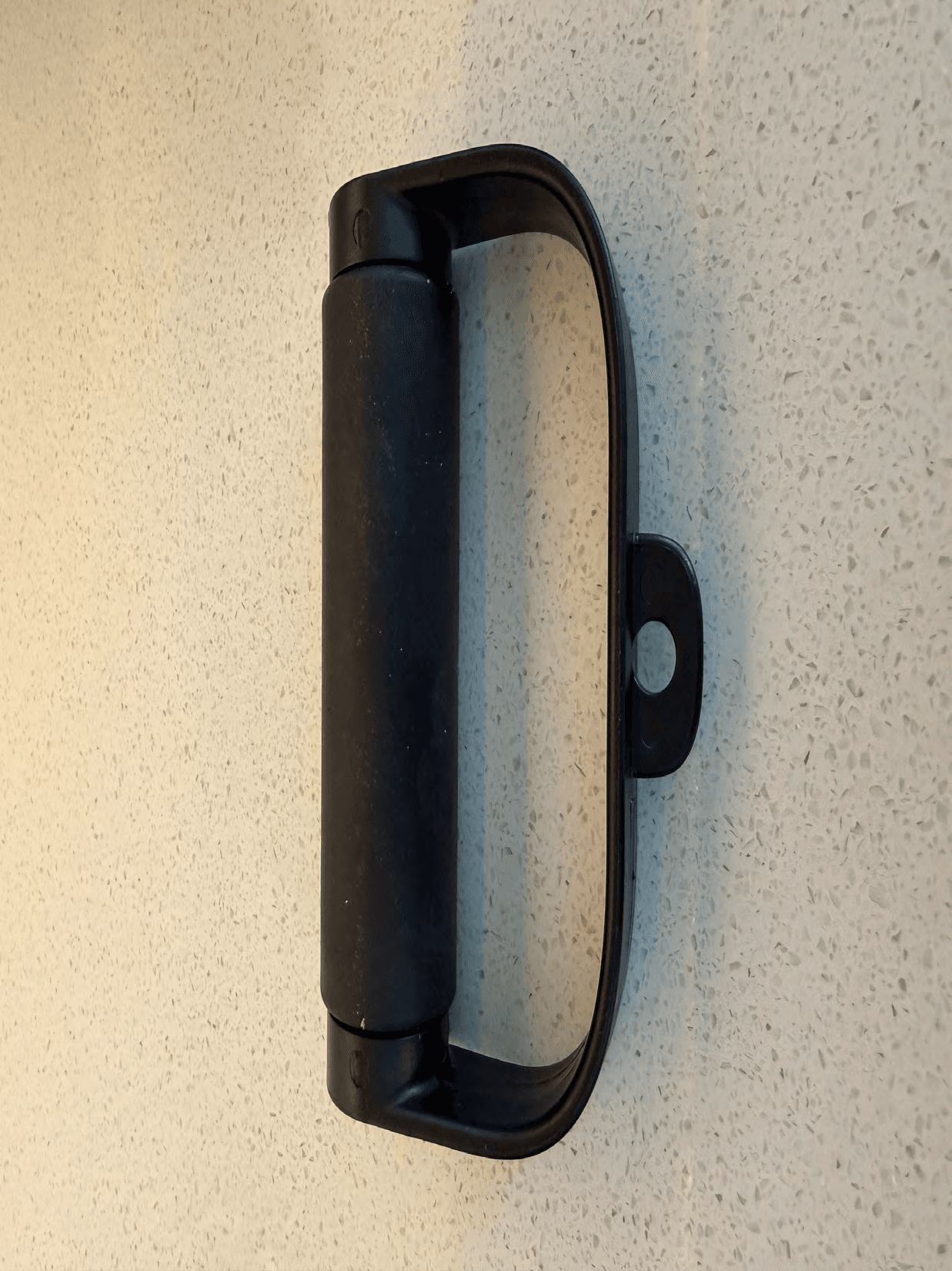
Click to zoom
Application Details
- Equipment Class
- DTS - Digital Transmission System
- Date of Grant
- May 20, 2026
- Application Purpose
- Original Equipment
- Equipment Note
- Health Monitoring therapy band
- Frequency Range
- 2402.00000000 - 2480.00000000
- Company
- Band Connect Inc.
- Country
- United States
Documents & Files
Document Text
Text extracted from the exhibit documents filed with the FCC. Open a document above to read the original.
Users Manual
Need help? Contact Band Connect at (513) 202-3370. 1 Quick Start Guide [email protected] (513)202-3370 © Band Connect, Inc. | [email protected] Getting Started Welcome to Band Connect! Hello, Welcome to Band Connect, your personalized therapy companion, designed to guide your recovery journey and help you achieve the best possible outcomes. With Band Connect, your home exercise program becomes straightforward and easy to follow. The app provides step- by-step instructions, real-time feedback to ensure correct form, and guidance aligned with what your clinician prescribed during your in-clinic visit. Your clinician can also monitor your progress, adjust your plan as needed, and ensure your recovery stays on track. Band Connect maximizes your recovery potential and by using this platform consistently, you’ll give your care team the insights they need to support your recovery every step of the way. Remember: bring your kit to every visit—it’s an essential part of your care. Let’s get started on the path to recovery, together. Best wishes, The Band Connect Team Need help? Contact Band Connect at (513) 202-3370. 3 What to Expect. You will leverage Band Connect both inside the clinic and at home. Here are the steps that you will take on your recovery journey. 1. 2. 3. FIRST IN-CLINIC VISIT Your clinician will set the base- lines for your exercises. AT-HOME SESSIONS Perform exercises at home with real-time feedback. Then, complete your assigned assessments. FOLLOW-UP IN-CLINIC VISITS Your clinician reviews progress and updates your home exercise program as needed. © Band Connect, Inc. | [email protected] Your Band Connect Kit contains all the essential components you will need for your recovery journey with Band Connect. So, let’s go over what’s inside. YOUR BAND CONNECT KIT 1. Band Connect Handle 2. Charging Cords 3. Charging Block 4. Phone Stand 5. Door Anchor 6. Carabiners Getting Started 4 6 1 5 2 1 3 Need help? Contact Band Connect at (513) 202-3370. 5 Find Band Connect on the App Store or Google Play to download the app, or scan the QR codes below for direct access. HOW TO DOWNLOAD THE APP Look for the Band Connect logo before downloading. Android Google Play Apple App Store © Band Connect, Inc. | [email protected] LOGGING IN 1. Login to the Band Connect App Input your username, which is the email you provided to your clinician, and the password you set in the clinic, then select “sign in”. If you don’t remember which email you provided to your clinician, please call Band Connect support at (513)202-3370. 2. Input your One Time Password (OTP) Once you complete the step above, you will receive an email with a four-digit code that you need to enter each time you log in. This is to keep your account secure. Once the app is downloaded, you can log in to access your treatments within the app. Getting Started Need help? Contact Band Connect at (513) 202-3370. 7 CONNECTING HANDLES 1. Find your handles in your kit. 3. Connect your handles to your phone. Your app will indicate the handles are connected. Your handles are the essential component in your kit. Please see below for how to use them properly and recommended best practices. 2. Turn on your Cuff. The Cuff will have a blue light when on. Solid blue indicates that you’re connected to your phone. BLUE Blinking green indicates charging, while a solid green light indicates the battery is fully charged. GREEN Blinking red indicates low battery. RED © Band Connect, Inc. | [email protected] Each day you log into the patient app, you will see the treatment that needs to be completed that day, including both the exercise sessions and assessments. START YOUR SESSION 1. Complete Exercise Session #1 First, select Session 1 on the assigned treatment screen to begin. Then follow the prompts to complete all exercises in Session 1. 2. Complete Additional Exercise Sessions After Session 1, proceed to the next available sessions, if any. Please follow directions from your clinician as to the interval between sessions. 3. Complete all assigned Assessments. Select “Assessments” on the treatment screen. Follow the prompts to answer the assessment questions as presented. Completing Your Treatment Need help? Contact Band Connect at (513) 202-3370. 9 The Band Connect app is very simple to use. The next section outlines what you will see while you’re completing your assigned treatment. 1. Pausing your session If interrupted, select the pause button to resume later. To skip an exercise, pause and select “Skip.” Choose a reason from the dropdown menu. 2. Movement Cues While completing your therapy, you’ll see cues such as “too fast,” “too slow,” “too short,” or “too far”. These are to help guide you to recreate what you did in the clinic with your clinician. WHAT YOU’LL SEE © Band Connect, Inc. | [email protected] Completing Your Treatment 3. Adjusting Tension The app ensures that you start with the right starting tension for each exercise that leverages the resistance band. Use the app’s tension bar to match the resistance band tension. 4. Haptic Feedback Handles buzz to signal when to start, pause, or end movements. Stronger feedback indicates incorrect handle positioning or movement. WHAT YOU’LL SEE The Band Connect app is very simple to use. The next section outlines what you will see while you are completing your assigned treatment. Need help? Contact Band Connect at (513) 202-3370. 11 COMPLETING AN UNCONNECTED SESSION If one or both handles do not connect to the application or get disconnected, you will be prompted to try to connect/reconnect the sensors. If you decide to continue without the connection, you have the ability to reconnect at any point by selecting “Connect Now”. You have the option to select continue to begin an unconnected session. © Band Connect, Inc. | [email protected] USING YOUR HANDLES 1. Keep Handles Charged Check the handle charge in the app (upper left corner). Charge handles at least on…
Text truncated - open the document above for the full version.
Attestation Statements
April 5, 2026 Federal Communications Commission Authorization and Evaluation Division 7435 Oakland Mills Road Columbia, MD 21046 USA Re: Covered List, located at https://www.fcc.gov/supplychain/coveredlist and 47 CFR parts §2.903 and §2.911(d)(5)(i)(ii) of the FCC rules Applicant: Band Connect Inc. FCC ID: 2BVEW-BC1 To whom it may concern, Band Connect Inc., (“Applicant”) certifies that the equipment for which authorization is sought is not “covered” equipment prohibited from receiving an equipment authorization pursuant to 47 CFR part §2.903 of the FCC rules and does not originate directly or indirectly from any company named on the covered list located in the link above or any subsidiary or affiliate thereof. Applicant further certifies that, as of the date of the filing of the application, the Applicant is not identified on the Covered List as an entity producing “covered” equipment and is not a subsidiary or affiliate of any such entity pursuant to 47 CFR part §1.50002 and required by 47 CFR part §2.911(d)(5)(ii) of the FCC rules. Applicant further certifies that no Cybersecurity or anti-virus software produced or provided by Kaspersky Lab, Inc. or any of its successors and assignees, including equipment with integrated Kaspersky Lab, Inc. (or any of its successors and assignees) cybersecurity or anti-virus software is installed in the equipment being certified. I HEREBY CERTIFY THAT I am authorized to make the representations above on behalf of the Applicant and agree to immediately notify Compliance Testing LLC if there is any change in the status identified above. Rohit Nayak Cofounder | Band Connect Inc. © Band Connect, Inc. | PAGE 1 2026-04-12 Audit trail Details FILE NAME Band Connect Attestation Statements part 2.911_d__5__i_ and 2.911_d__5__ii_ filing.docx - 4/12/26, 3:38 PM STATUS Signed STATUS TIMESTAMP 2026/04/12 19:41:52 UTC Activity SENT [email protected] sent a signature request to: Rohit Nayak ([email protected]) 2026/04/12 19:38:14 UTC SIGNED Signed by Rohit Nayak ([email protected]) 2026/04/12 19:41:52 UTC COMPLETED This document has been signed by all signers and is complete 2026/04/12 19:41:52 UTC The email address indicated above for each signer may be associated with a Google account, and may either be the primary email address or secondary email address associated with that account.
Attestation Statements
04-05-2026 Federal Communications Commission Authorization and Evaluation Division 7435 Oakland Mills Road Columbia, MD 21046 USA Ref: Attestation Statements Part 2.911(d)(7) Filing FCC ID or Grantee Code: 2BVEW-BC1 Band Connect Inc., (“the applicant”) certifies that, as of the date of the filing of the application, we designate ourselves as the U.S. agent for service of process. Designated U.S. Agent Information: FRN: 0038212742 Name: Band Connect Inc. Address: 1116 Race Street, Cincinnati, OH 45202 Contact Person: Rohit Nayak Tel.: 513-293-4942 Email: [email protected] Sincerely, Rohit Nayak Cofounder | Band Connect Inc. © Band Connect, Inc. | PAGE 1 2026-04-12 Audit trail Details FILE NAME Band Connect Attestation Statements US agent for service of process - Applicant self designation.docx - 4/12/26, 3:38 PM STATUS Signed STATUS TIMESTAMP 2026/04/12 19:41:22 UTC Activity SENT [email protected] sent a signature request to: Rohit Nayak ([email protected]) 2026/04/12 19:39:07 UTC SIGNED Signed by Rohit Nayak ([email protected]) 2026/04/12 19:41:22 UTC COMPLETED This document has been signed by all signers and is complete 2026/04/12 19:41:22 UTC The email address indicated above for each signer may be associated with a Google account, and may either be the primary email address or secondary email address associated with that account.
Cover Letter(s)
April 13, 2026 Federal Communications Commission Authorization & Evaluation Division 7345 Oakland Mills Road Columbia, Maryland 21046 RE: LETTER OF AGENT AUTHORIZATION To Whom It May Concern: We, the undersigned, hereby authorize Compliance Testing, LLC to act on our behalf in all matters relating to application for equipment authorization, including the signing of all documents relating to these matters. We also hereby certify that no party to the application authorized hereunder is subject to the denial of benefits, including FCC benefits, pursuant to Section 5301 of the Anti-Drug Abuse Act of 1988, 21 U.S.C.853(a). Sincerely, Rohit Nayak Cofounder, Band Connect Inc. 513-293-4942 | www.bandconnect.net © Band Connect, Inc. | PAGE 1 Audit trail Details FILE NAME Band Connect FCC Agent Authorization.docx - 4/12/26, 6:16 PM STATUS Signed STATUS TIMESTAMP 2026/04/12 22:17:09 UTC Activity SENT [email protected] sent a signature request to: Rohit Nayak ([email protected]) 2026/04/12 22:16:13 UTC SIGNED Signed by Rohit Nayak ([email protected]) 2026/04/12 22:17:09 UTC COMPLETED This document has been signed by all signers and is complete 2026/04/12 22:17:09 UTC The email address indicated above for each signer may be associated with a Google account, and may either be the primary email address or secondary email address associated with that account.
Cover Letter(s)
April 5, 2026 Federal Communications Commission Authorization & Evaluation Division 7345 Oakland Mills Road Columbia, Maryland 21046 RE: Long-Term Confidentiality Request for Band Connect BCUE1 / FCC ID: 2BVEW-BC1 To Whom It May Concern: This letter serves as an official request for confidentiality under § 0.457(d) and § 0.459 of CFR 47. We have requested that the following documents required to be submitted with this application be permanently withheld from public review. ● Block Diagram ● Schematics ● Theory of Operation ● Tune Up Procedure ● Parts List/BOM These documents contain detailed system and equipment descriptions and related information about the product, which manufacturer/applicant considers to be proprietary, confidential, and a custom design and otherwise, would not release to the general public. Since this design is a basis from which future technological products will evolve, manufacturer/applicant feels that this information would be of benefit to its competitors, and that the disclosure of the information in these documents would give our competitors an unfair advantage in the market. Please contact me if there is any information you may need. Sincerely, Rohit Nayak Cofounder, Band Connect Inc. 513-293-4942 | www.bandconnect.net © Band Connect, Inc. | PAGE 1 2026-04-12 Audit trail Details FILE NAME Band Connect FCC Long-Term Confidentiality Request.docx - 4/12/26, 3:39 PM STATUS Signed STATUS TIMESTAMP 2026/04/12 19:40:45 UTC Activity SENT [email protected] sent a signature request to: Rohit Nayak ([email protected]) 2026/04/12 19:39:56 UTC SIGNED Signed by Rohit Nayak ([email protected]) 2026/04/12 19:40:45 UTC COMPLETED This document has been signed by all signers and is complete 2026/04/12 19:40:45 UTC The email address indicated above for each signer may be associated with a Google account, and may either be the primary email address or secondary email address associated with that account.
Internal Photos
Test Setup Photos FCC ID: 2BVEW-BC1 P25c0011_Filing Photos _Rev 2.0 Internal PCB Photo – Bottom surface Internal PCB Photo – Top surface Test Setup Photos FCC ID: 2BVEW-BC1 P25c0011_Filing Photos _Rev 2.0 Internal PCB Photo – Antenna Placement Internal PCB Photo – Bottom surface
RF Exposure Info
P25c0011_FCC_MPE_Rev 1.0 Page 1 of 6 Test Report Prepared for: Band Connect Model: BCUE1 Project No: p25c0011 Serial Number: TST_RF_UFL_1, TST_RF_ANT_1 FCC ID: 2BVEW-BC1 To FCC Part 1.1310 FCC Part 2.1093 447498 D04 Interim General RF Exposure Guidance v01 Date of Issue: February 20, 2026 On behalf of the applicant: Band Connect 1116 Race Street Cincinnati, OH, 45202 Attention of: Rohit Nayak Ph: (513)-293-4942 E-mail: [email protected] Prepared By: Compliance Testing, LLC Mesa, AZ 85204 (480) 926-3100 phone / (480) 926-3598 fax www.compliancetesting.com ANAB Cert#: AT-2901 FCC Site Reg. #750616 ISED Site Reg. #2044A-2 Reviewed / Authorized By: Harshith Devaraja EMC Engineer This report may not be reproduced, except in f ull, without written permission f rom Compliance Testing All results contained herein relate only to the sample tested P25c0011_FCC_MPE_Rev 1.0 Page 2 of 6 Test Report Revision History Revision Date Revised By Reason for Revision 1.0 February 20, 2026 Harshith Devaraja Original Document Current revision of the test report replaces any prior versions. Only the current version of the test report is valid. P25c0011_FCC_MPE_Rev 1.0 Page 3 of 6 EUT Description Model: BCUE1 Serial: TST_RF_UFL_1, TST_RF_ANT_1 Firmware: Application core v11 Firmware: BLE module core 1.17.0 Description: Health Monitoring therapy band Additional Information: Radio Frequency Range and Operational Info: 2.4 – 2.4835 GHz BLE GFSK (1Mbps & 2 Mbps) FCC Emission designator: 1M10F1D Antenna Gain = 1.95 dBi Usage: Portable Receipt of Sample(s): January 23, 2026 EUT Condition: Visual Damage No State of Development Production/Production Equivalent P25c0011_FCC_MPE_Rev 1.0 Page 4 of 6 Power calculations Antenna gain = 1.95 dbi EIRP = Conducted peak power (dBm) + Antenna gain (dBi) Tuned Frequency (MHz) Conducted Peak Output Power (dBm) Conducted Peak Output Power (mW) EIRP (dBm) EIRP (mW) 2402 0.76 1.2 2.71 1.866 2440 1.70 1.5 3.65 2.317 2480 1.45 1.4 3.4 2.1877 P25c0011_FCC_MPE_Rev 1.0 Page 5 of 6 MPE Evaluation This is a portable device used in Uncontrolled Exposure environment. Limits Controlled Exposure 47 CFR 1.1310 Table 1, (A) 0.3-3.0 MHz: Limit [mW/cm²] = 100 3.0-30 MHz: Limit [mW/cm²] = (900/f ²) 30-300 MHz: Limit [mW/cm²] = 1.0 300-1500 MHz: Limit [mW/cm²] = f /300 1500-100,000 MHz Limit [mW/cm²] = 5 Limits Uncontrolled Exposure 47 CFR 1.1310 Table 1, (B) 0.3-1.234 MHz: Limit [mW/cm²] = 100 1.34-30 MHz: Limit [mW/cm²] = (180/f ²) 30-300 MHz: Limit [mW/cm²] = 0.2 300-1500 MHz: Limit [mW/cm²] = f /1500 1500-100,000 MHz Limit [mW/cm²] = 1.0 Test Data Test Frequency, MHz 2440 Conducted peak Power, mW (P) 1.5 Antenna Gain Isotropic 1.95 dBi Antenna Gain Numeric (G) 1.57 Distance (R) 0.5 cm 푆= 푃∗퐺 4휋푟 2 Power Density (S) mw/cm 2 Power Density (S) = 0.7496 mw/cm 2 Limit = (f rom above table) = 1.0 mw/cm 2 P25c0011_FCC_MPE_Rev 1.0 Page 6 of 6 Determination of Exemption 47 CFR 2.1093 (c)(1) ERP20cm = 3060 mW Separation distance (d) = 0.5 cm Calculated Pth = 2.753 mW Tuned Frequency (MHz) Conducted Peak Output Power (dBm) Conducted Peak Output Power (mW) EIRP (dBm) EIRP (mW) ERP=EIRP-2.15 (dBm) ERP (mW) 2440 1.70 1.5 3.65 2.317 0.167 1.0392 ERP of the EUT = 1.0392 mW ERP EUT < Calculated Pth : Result:- Pass The portable EUT is SAR test exempt. END OF TEST REPORT
Test Report
P25c0011_FCC_Part 15.247_Rev 1.0 Page 1 of 80 Test Report Prepared for: Band Connect Model: BCUE1 Serial Number: TST_RF_UFL_1, TST_RF_ANT_1 Project No: p25c0011 FCC ID: 2BVEW-BC1 To FCC Part 15.247 Test Results: Pass Date of Issue: February 20, 2026 On the behalf of the applicant: Band Connect 1116 Race Street Cincinnati, OH, 45202 Attention of: Rohit Nayak Ph: (513)-293-4942 E-mail: [email protected] Prepared By: Compliance Testing, LLC Mesa, AZ 85204 (480) 926-3100 phone / (480) 926-3598 fax www.compliancetesting.com ANAB Cert#: AT-2901 FCC Site Reg. #750616 ISED Site Reg. #2044A-2 Reviewed / Authorized By: Harshith Devaraja, EMC Engineer This report may not be reproduced, except in full, without written permission from Compliance Testing. All results contained herein relate only to the sample tested. All samples were selected by the customer. P25c0011_FCC_Part 15.247_Rev 1.0 Page 2 of 80 Test Results Summary Test Date Range: February 16, 2026 – February 20, 2026 Specification Test Name Pass, Fail, N/A Comments FCC 15.247(a)(2) Occupied Bandwidth Pass 15.247(b)(3) Transmitter Output Power Pass 15.247(d) Conducted Spurious Emissions Pass 15.247(d), 15.209(a), 15.205 Radiated Spurious Emissions Pass 15.247(d), 15.209(a), 15.205 Emissions At Band Edges Pass 15.247(e) Power Spectral density Pass 15.207 A/C Powerline Conducted Emissions Pass 15.203 Antenna Requirement Pass Method Deviations/Additions: No Statements of conf ormity are reported as: • Pass - the measured value is below the acceptance limit, acceptance limit = test limit. • Fail - the measured value is above the acceptance limit, acceptance limit = test limit. References/Methods Description ANSI C63.4-2014 Method and Measurements of Radio-Noise Emissions from low-Voltage Electrical and Electronic Equipment in the range 9kHz to 40GHz. ANSI C63.10:2020 American National Standard of Procedures f or Compliance Testing of Unlicensed Wireless Devices 558074 D01 15.247 Meas Guidance v05r02 Guidance f or Compliance Measurements on DTS, FHSS, and Hybrid System Devices Operating Under Section 15.247 of the FCC Rules ISO/IEC 17025:2017 General requirements for the Competence of Testing and Calibrations Laboratories P25c0011_FCC_Part 15.247_Rev 1.0 Page 3 of 80 Table of Contents Description Page Test Results Summary ....................................................................................................... 2 Test Report Revision History ............................................................................................... 4 EUT Description ................................................................................................................ 5 Test and Measurement Data ............................................................................................... 7 Test Setup and Modes of Operation ..................................................................................... 8 Transmitter Output Power ..................................................................................................10 Radiated Spurious Emissions .............................................................................................18 Restricted Band Edges ......................................................................................................49 Occupied Bandwidth .........................................................................................................54 Power Spectral Density .....................................................................................................62 Conducted Spurious Emissions ..........................................................................................70 AC Line Conducted Emissions............................................................................................77 Test Equipment Utilized .....................................................................................................80 Measurement Uncertainty ..................................................................................................80 P25c0011_FCC_Part 15.247_Rev 1.0 Page 4 of 80 Test Report Revision History Revision Date Revised By Reason for Revision 1.0 February 20, 2026 Harshith Devaraja Original Document Current revision of the test report replaces any prior versions. Only the current version of the test report is valid. P25c0011_FCC_Part 15.247_Rev 1.0 Page 5 of 80 EUT Description Model: BCUE1 Serial: TST_RF_UFL_1, TST_RF_ANT_1 Firmware: Application core v11 Firmware: BLE module core 1.17.0 Description: Health Monitoring therapy band Additional Information: Radio Frequency Range and Operational Info: 2.4 – 2.4835 GHz BLE GFSK (1Mbps & 2 Mbps) Usage: Portable Receipt of Sample(s): September 17, 2025 EUT Condition: Visual Damage No State of Development Production/Production Equivalent P25c0011_FCC_Part 15.247_Rev 1.0 Page 6 of 80 The applicant has been cautioned as to the following 15.21 - Information to User The user’s manual or instruction manual for an intentional radiator shall caution the user that changes or modifications not expressly approved by the party responsible for compliance could void the user’s authority to operate the equipment. 15.27(a) - Special Accessories Equipment marked to a consumer must be capable of complying with the necessary regulations in the conf iguration in which the equipment is marketed. Where special accessories, such as shielded cables and/or special connectors are required to enable an unintentional or intentional radiator to comply with the emission limits in this part, the equipment must be marketed with, i.e. shipped and sold with, those special accessories. However, in lieu of shipping or packaging the special accessories with the unintentional or intentional radiator, the responsible party may employ other methods of ensuring that the special accessories are provided to the consumer without an additional charge. Inf ormation detailing any alternative method used to supply the special accessories f or …
Text truncated - open the document above for the full version.
Test Report
Introduction This application note is dedicated to the STM32WB Series microcontrollers. One of the main reasons to use a PCB (printed circuit board) antenna is the reduced overall cost of the radio module. Well designed and implemented PCB-printed antennas have a similar performance to the SMD (surface-mounted device) ceramic equivalence. In general, the footprint for a ceramic SMD antenna is smaller than that for a PCB-printed variant. For a PCB-printed antenna solution, the increased size of the PCB in relation to space required for the antenna means that the radio module is larger and the cost of the PCB increased. However the PCB solution is generally cheaper than a SMD ceramic antenna. The demonstration and development boards for the STM32WB Series implement PCB printed antenna based on this application note. Low cost PCB antenna for 2.4 GHz radio: meander design for STM32WB Series AN5129 Application note AN5129 - Rev 4 - April 2019 For further information contact your local STMicroelectronics sales office. www.st.com 1General information This document applies to STM32WB Series Arm ® -based devices. Note:Arm is a registered trademark of Arm Limited (or its subsidiaries) in the US and/or elsewhere. AN5129 General information AN5129 - Rev 4 page 2/22 2Coordinate system For the purpose of this document, the spherical coordinate system illustrated in the figure below is used. Figure 1. Spherical coordinate system The PCB module is orientated vertically (plane X-Z) and located in proximity to the origin of the coordinate system. The azimuth angle radiates from the X-axis towards the Y-axis and the elevation angle radiates from the Z-axis towards the horizontal X-Y plane. Sometimes, as with geographical and navigational systems, the X-axis is called the "Nord-axis", the Yaxis is called the "East-axis" and the Z-axis is called the "Zenith-axis". AN5129 Coordinate system AN5129 - Rev 4 page 3/22 3Layout specification The PCB antennas, including the electrical parameters of PCB materials used, are layout sensitive. It is recommended to use a layout as close as possible to the one shown in the figure below. Figure 2. PCB antenna dimensions (in mm) The electrical parameters and performance of the PCB antenna are also determined by the substrate used, in particular the thickness of the core and dielectric constants. AN5129 Layout specification AN5129 - Rev 4 page 4/22 The figure below illustrates a typical cross-section of the substrate in a PCB-antennae area. Figure 3. PCB cross section at antennae area A substrate with the parameters as defined in the table below is recommended. Table 1. Recommended substrate specification Layer Dimensions Dielectric constant Ɛ R LabelValue (mil)Value (μm) Solder mask, topS10.717.784.4 Copper traceT1.640.64- CoreC28711.24.4 Solder mask, bottomS20.717.784.4 AN5129 Layout specification AN5129 - Rev 4 page 5/22 4Impedance matching Meander-like PCB antenna can be tuned to the required 50 Ω impedance by matching the impedance circuitry with the π topology. In Figure 2, the impedance matching area is marked with a dashed line. Under nominal conditions, this antenna exhibits and impedance very close to the required nominal impedance (50 Ω). To check the performance of this design, a sample antenna was manufactured (according to the specifications covered by this document). The figure below shows this antenna. Figure 4. Part of 802.15.4 and BLE PCB with meander-like antenna (scale around 4:1) Assuming that the manufactured sample exhibits the expected performance (no impedance matching necessary), the impedance matching circuitry is bypassed by two 100 pF capacitors connected in series, as shown in the figure below. Figure 5. Bypassing impedance matching circuitry - Direct RF connection All electrical parameters of the meander-like antenna have been measured at connection to the band-pass filter (BPF) with the frequency span covering frequencies from 2.4 GHz to 2.5 GHz. AN5129 Impedance matching AN5129 - Rev 4 page 6/22 Complex impedance of the antenna is shown in the Smith diagram in the figure below. Figure 6. Complex impedance of the meander-like antenna (Smith chart) The figure below shows the magnitude of the S11 parameter (in log scale). Figure 7. S11 parameter in logarithmic scale (Cartesian plot) AN5129 Impedance matching AN5129 - Rev 4 page 7/22 The figure below shows the standing wave ratio (SWR). Figure 8. Antenna standing wave ratio (SWR) The following changes affect the radiation impedance of the PCB antenna: • slight board size variation • metal shielding • use of plastic cover • presence of other components in proximity of the antenna The best performance impedance matching circuitry compensates these effects so that, for operating frequencies, the optimum 50 Ω impedance is achieved. AN5129 Impedance matching AN5129 - Rev 4 page 8/22 5Radiation pattern, 3-D visualization A three-dimensional (3-D) visualization of the radiation pattern (magnitude of the electrical far field |E|) is done for the center ISM band frequency 2.44175 GHz. Figure 9. 3-D radiation pattern overview Figure 10. Radiation pattern on X-Z plane AN5129 Radiation pattern, 3-D visualization AN5129 - Rev 4 page 9/22 6Radiation pattern, 2-D visualization In this section, all radiation patterns are related to the magnitude of electrical far field |E|, that is normalized and shown in the logarithmic scale (in dB). This means that the maximum global radiation pattern (maximum magnitude of the electrical far-field E) is represented by 0 dB level. To show the antenna radiation patterns in detail, three two dimensional (2-D) major cuts are presented. Consider the orientation of the module in the spherical coordinate system as shown in Figure 1. A three dimensional (3-D) far field radiation pattern is visualized as three two dimensional (2-D) cuts through a 3- D pattern. The following major planes are used for these cuts (see Figure 11): • one horizontal X-Y plane • two vertical planes: X-Z plan…
Text truncated - open the document above for the full version.
Test Setup Photos
Test Setup Photos FCC ID: 2BVEW-BC1 P25c0011_Filing Photos _Rev 2.0 30-1000 MHz Radiated Emissions Setup 1-18 GHz Radiated Emissions Setup Test Setup Photos FCC ID: 2BVEW-BC1 P25c0011_Filing Photos _Rev 2.0 18-26 GHz Radiated Emissions Setup Worst Case Orientation Test Setup Photos FCC ID: 2BVEW-BC1 P25c0011_Filing Photos _Rev 2.0 AC Power line Conducted Test Setup 1 AC Power line Conducted Test Setup 2
Contact Information
Applicant
Rohit Nayak(Cofounder)
[email protected]Fax: 5132934942
Technical Contact
Band Connect Inc.Rohit Nayak
1116 Race Street · Cincinnati, Ohio, 45202 · United States
Test Firm
Compliance Testing, LLCMichael Schafer
Technical Specifications
| # | Rule Parts | Frequency Range | Power Output |
|---|---|---|---|
| 1 | 15C | 2.40 GHz - 2.48 GHz | 1.50 mW |